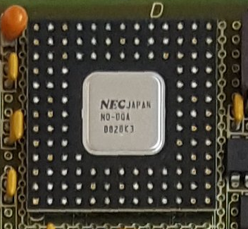
NEC Decode Gate Array
The Decode Gate Array (DGA) is described in a PDF spanning 19 pages
DGA Circuits
The decoder diagrams are all in one file: ND_DGA
Status of Logisim drawings from DGA Schematics PDF
- Helper circuits needs to be validated
- All circuits needs to be tested
| Page name | PDF page number(s) | Status | Comment |
|---|---|---|---|
| DECODE_DGA | 1-7 (8 pages) | OK | |
| DECODE_DGA_POW | 8-10 (3 pages) | OK | |
| DECODE_DGA_PFIFD | 11 (1 page) | OK | |
| DECODE_DGA_PFIFC | 12 (8 pages) | OK | |
| DECODE_DGA_PFIFC_DELAY | 13 (1 page) | OK | |
| DECODE_DGA_IDBS | 14-15 (2 pages) | OK | |
| DECODE_DGA_COMM | 16-19 (4 pages) | OK |
Helper Circuits
Details found in the NEC User's Manual
- CMOS-8L Family CMOS Gate Array
- Block Library Ver 5.0
- File: REN_A12213XJ5V1UM00_OTH_19980801.PDF
| Circuits name | Description | Status |
|---|---|---|
| F091 | Level Generator | OK |
| F103 | Inverter | OK |
| F571 | 2 to 1 MULTIPLEXER POSITIVE OUTPUT WITH ENABLE | OK |
| F595 | RS-LATCH | OK |
| F617 | D Flip-Flop with RB an SB | OK |
| F924 | 4-BIT D Flip-Flop | OK |
| F714 | T Flip-Flop with R an S | OK |
| F774 | JK-F/F WITH R,S | OK |