IO / REG
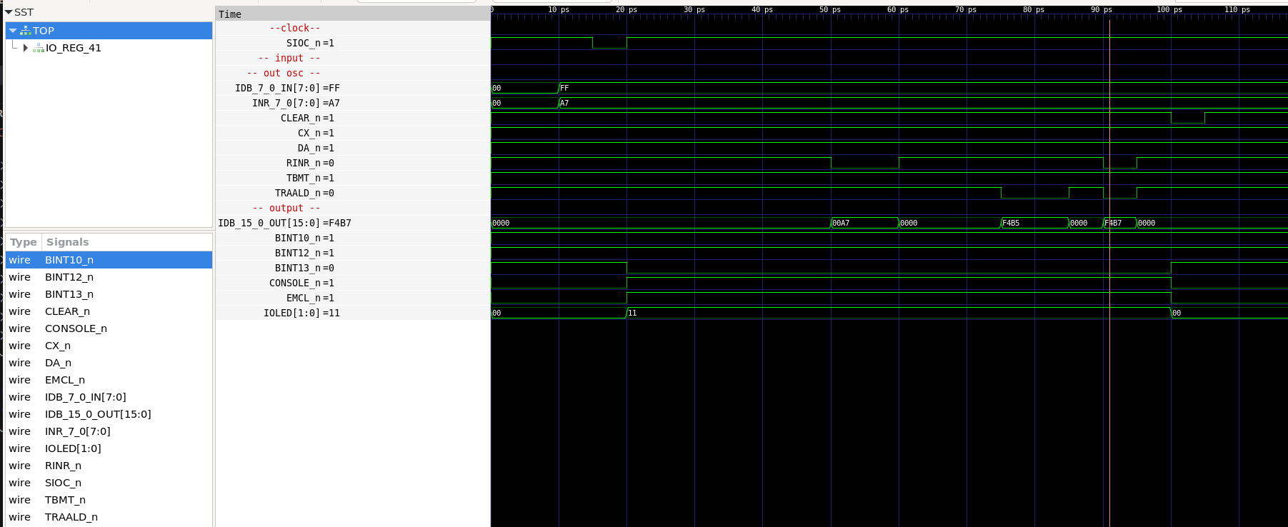
IOC, ALD and INR regs
- Write to IDB = 0xFF;
- Write to INR = 0xA7;
- Latch 0xFF to IOC (chip 28A) => Change signals for SCONS,EMCL, LED2,LED3, IOC3:0
- Read INR => IDB OUT = 0xA7
- Stop reading => IDB OUT = 0
- Read ALD => IDB OUT = 0xF4B5
- Read both INR and ALD at the same time to validate that output is OR'ed together => IDB OUT = 0xF4B7
- Clear IOC chip by setting CLEAR_n low
CPU Board 3202D - Sheet 41
Test program verification