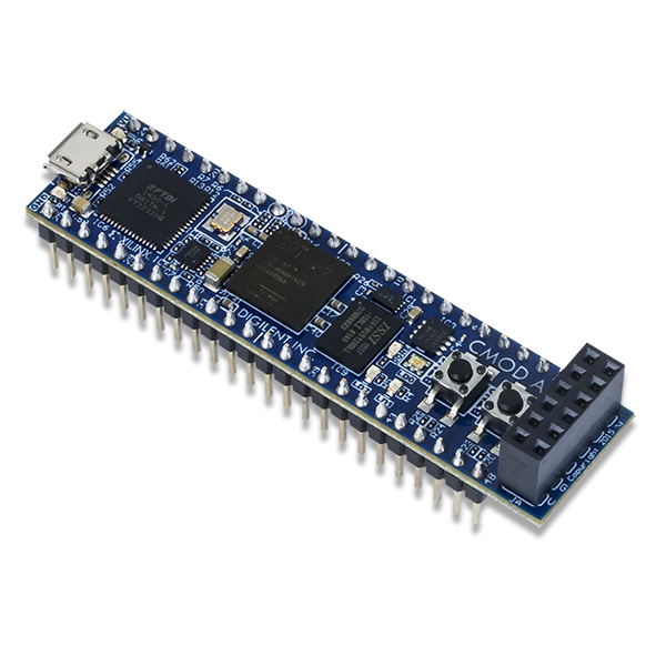
ND-120 on Digilent Cmod A7-35T
Full path: Verilog/fpga/cmod-a7-35t/
Status
ACTIVE - the owner has the board. First built 04-SEP-2026 (the build files had sat unrun since 13-JUL). Configuration: block-RAM main memory, CPU at 27 MHz, console on the on-board USB chip; see "First build" below.
It fits the part easily and does NOT meet timing: WNS -89.814 ns at 27 MHz.
No bitstream is written, because build.tcl refuses to write one on negative
slack. The cause is the CGA IDB combinational ring, not this board and not
this clock - full diagnosis under "Build history". Until the ring is cut in
RTL, this board cannot be signed off by its own timing gate, and lowering the
clock would only fit the clock to a tool artifact.
The 512 KB SRAM main-memory upgrade is specified in
SRAM-BRIDGE-PLAN.md (pack16, <= 33 MHz validated -
see Verilog/docs/basys3-memory-speed-validation.md).
Board docs live with the board, not in Verilog/docs/.
Build history - FIRST BUILT 04-SEP-2026
The build files sat unbuilt from 13-JUL to 04-SEP-2026. Two things were wrong
with them, both found on the first run and both now fixed in build.tcl:
- Missing include paths. Synthesis stopped with 17 errors before touching
any logic:
cannot open include file 'nd_storage_status.vh'and'nd120_backwiring_defaults.vh', then a cascade of undefined-macro errors inND_FLOPPY_DMA.v. Both headers were added to the tree after this script was written. Fixed by passingSD-FAT/circuitandShared/supporttosynth_design -include_dirs, as the Nexys and MEGA65 builds already do. -
Timing, badly, and NOT for the reason it first looked like. With the includes fixed the design placed and routed at a comfortable 5,285 of 20,800 LUTs (25.4%) and 2,494 of 41,600 registers - MEASURED from its own
util.rpt, which is the CPU plus block-RAM memory and nothing else; for scale the Nexys hierarchical report puts the whole ND-120 CPU board at 3,186 LUTs / 1,879 FFs. A figure of "11,493 LUTs and 26.5 of 50 block RAM tiles" stood here and was WRONG. It then missed timing by 95.488 ns at 27 MHz - 5133 of 18465 endpoints failing. The Inter Clock Table was EMPTY, so the clock groups were working.The first worst path ended at the microcode PROM's data register, which suggested the runtime PROM-to-WCS load (this was the last build still using it).
SKIP_WCS_LOADwas made the default here, as on every other board. It bought 5.7 ns: -95.488 -> -89.814 ns. That hypothesis was wrong, and the change is kept only because it is right on its own merits (the PROM's ROM is not built at all).-promloadrestores the old path.The real cause, from the routed checkpoint: all 200 worst paths share ONE start and ONE end -
CPU/CS/WCS/CHIP_21CtoCPU/PROC/CGA/DELILAH/MAC/MAC_LA1025/R_LA_L, 234 logic levels, 126.5 ns, running through the ALU and never touching main memory. The build reports 16[DRC LUTLP-1]combinatorial-loop critical warnings and 23 auto-inserted loop-breaking false paths, and the loops named in them are the CGA IDB ring exactly asDELILAH-CPU/CGA/circuit/CGA.v:700-745describes it:ALU_OUTMUX/OUTMUX_IDBS/IDBS_R1/D_15_0[n]->G_15_0[n]-> FIDBO -> MAC/INTR -> back.So the 234-level path is where Vivado happened to cut a loop, not a real microcycle. Per-board logic levels on the comparable path, with what each figure actually rests on:
board levels verified Nexys 4 DDR @ 45.45 MHz 31 YES - fpga/nexys4ddr/timing-analysis/run_clk45/setup_paths_post_route.rpt:24QMTECH @ 20 MHz 49 YES - fpga/qmtech-a35t/timing.rpt:431Cmod A7 @ 27 MHz 234 YES - top5_paths.rpt, 5 paths agreeMEGA65 R6 58 NO - prose only MEGA65 R3 93 NO - prose only A "7 levels on the Nexys" figure stood here from 04-SEP-2026 and was WRONG - it came from a sentence, not a report. Anything argued on top of it (notably "the constrained boards have huge headroom") does not follow from the real numbers. See
docs/HANDOFF-cga-idb-ring-cut.mdsection 3a.This design also boots SINTRAN on the Tang, whose toolchain has no loop DRC at all. A lower clock does not fix this - now MEASURED, not estimated (07-SEP-2026). The same build at 13.5 MHz (
build.tcl -tclargs -slowclk):27 MHz 13.5 MHz clock period 37.037 ns 74.074 ns WNS -89.814 ns -48.963 ns data path delay 126.536 ns 122.594 ns logic levels 234 232 Halving the clock moved the path by 2 levels and 4 ns. The slack improved only because the period doubled; Vivado snips the loop in the same place either way, and the module breakdown of the two paths is the same ring (
OUTMUX_IDBS96 hops in BOTH builds,ALU_RALU/MUXQ334 in both). So the target clock does not steer the loop-break - that hypothesis is dead, and at 122.6 ns the CPU would have to run under 8.2 MHz, which is fitting the clock to an artifact rather than to the machine. The fix is to break the ring in RTL, and CGA.v:734-737 says what would work and records three attempts that were measured WORSE.
A routed checkpoint is now written before the timing gate
(nd120_cmod_routed.dcp), so a failing build can be interrogated without
paying for another run - the first 04-SEP failure could only report its single
worst path, which is exactly how the wrong hypothesis above survived as long
as it did. Interrogate it with:
open_checkpoint nd120_cmod_routed.dcp
report_timing -max_paths 50 -slack_lesser_than 0 -file paths.rpt
Note on capacity, so nobody plans a SINTRAN machine around this board: the 512 KB SRAM upgrade gives 256K ND words. SINTRAN's working boards all have 2M words. The one documented hard requirement is memory above 0o200000 (64K words), which 256K clears, but whether SINTRAN runs in 256K words is not measured anywhere. This is a test-program board plus an SD card unless that measurement says otherwise.
Build configuration: ND-120 CPU on BRAM at 27 MHz (misses timing - see Status)
Same configuration as the Basys3 build (FPGA_FF_MODE, MAIN_RAM_BLOCKRAM) but
self-contained (no Vivado GUI project) and clocked at 27 MHz. The microcode
now comes from the WCS preload (SKIP_WCS_LOAD), not the runtime PROM load -
see "Build history" for the timing measurement that forced the change:
cd Verilog/fpga/cmod-a7-35t
vivado -mode batch -source build.tcl                  # build + JTAG program
vivado -mode batch -source build.tcl -tclargs -noburn # build only
make / make build from WSL - Vivado path: ND120_VIVADO in
local.mk at the repository root, written by python3 configure.py; the
build folder ND120_BUILD_DIR too - everything the build writes goes to
$ND120_BUILD_DIR/cmod-a7-35t/. See
CONTRIBUTING.md - Local settings.)
- Clocking - how 27 MHz comes from the 12 MHz crystal: the
TARGET_CMOD_A7branch inVerilog/ND120_TOP.vsets the MMCM to VCO = 12 x 63 = 756 MHz (inside the 600-1200 MHz range), clk_cpu = 756 / 28 = 27.000 MHz exactly - soBOARD_CLK_FREQ=27000000and every UART/RTC count matches the Tang. (A PLL cannot be used - its minimum input is 19 MHz; the MMCM goes down to 10 MHz.) If 27 MHz does not close timing, build.tcl fails loudly on negative WNS; fallback is-verilog_define ND120_CMOD_MMCM_DIV=56.0= 13.5 MHz (halved, still faster than nothing - and change BOARD_CLK_FREQ to 13500000 to match). - Console: FT2232 COM port, 115200 8N1 (same as the Basys3 build).
- Buttons: BTN0 = reset. LEDs: LD0 = error/halt, LD1 = running; RGB (50% PWM per the manual's brightness warning): red = not-running, green = reset released, blue = UART TX.
- Main memory: BRAM, Basys3-equivalent default (3 banks x 4K words =
24 KB). Raising it toward the 32-64K-word ceiling =
BANK_ADDR_BITSinMEM_RAM_49_BLOCKRAM.v(+SKIP_WCS_LOADfor the top of the range) - see the capacity math inVerilog/docs/basys3-memory-speed-validation.mdsection 4.1.
SD-card Pmod on the single Pmod connector (JA)
The Digilent SD Pmods (Pmod MicroSD / Pmod SD - same mapping) plug
straight into JA. Wiring (Pmod pin -> JA pin -> FPGA pin, from
Cmod-A7-Master.xdc):
| Pmod pin | Signal | FPGA pin |
|---|---|---|
| 1 | ~CS / DAT3 | G17 |
| 2 | MOSI / CMD | G19 |
| 3 | MISO / DAT0 | N18 |
| 4 | SCK | L18 |
| 5, 11 | GND | - |
| 6, 12 | VCC = 3.3 V from the Pmod header | - |
| 7 | DAT1 | H17 |
| 8 | DAT2 | H19 |
| 9 | CD (card detect) | J19 (optional, unused by the stack) |
| 10 | (WP / NC) | K18 (unused) |
Voltage rules (do not skip):
- The Pmod header's VCC pins supply 3.3 V - correct for SD cards and both Digilent SD Pmods. Power the module ONLY from the Pmod header.
- Never power the SD module from VU (DIP pin 24) - VU is driven to ~5 V when USB is attached. SD cards are 3.3 V devices and the Cmod's FPGA pins are NOT 5 V tolerant.
- Note the reference-manual figure: VU's minimum rises with Pmod 3V3 load (3.38 V @ 100 mA, 3.48 V @ 250 mA drawn from the Pmod header) - an SD card's ~100 mA is within budget on USB power.
- In the XDC, enable internal pull-ups on CMD/DAT0-3 (
PULLUP true) - the stack needs released lines idling high (DAT3 high at CMD0 keeps the card out of SPI mode); the Pmod module's own pull-ups are not guaranteed. Same reasoning as the Basys3 port (Verilog/fpga/basys3/sd-fat-test/), which is also the wrapper template for a Cmod SD test build (swap the MMCM input for 12 MHz, pins from the table above).
Main-memory ceiling - MEASURED 07-SEP-2026
Neither this board nor the Basys3 can host the 64K words that standalone test programs want. The realistic ceiling is 24K words - a third of what is needed - and getting beyond that means removing working parts of the CPU, which is not a real option. This is a capacity fact, not a timing one, and it is entirely separate from the CGA IDB ring problem: fixing the ring would not add a single word.
The XC7A35T has 50 block-RAM tiles (~1,800 Kbit). Main memory is stored
16 bits wide with parity regenerated on read (MEM_RAM_49_BLOCKRAM.v:110),
so roughly 32 Kbit usable per tile.
Measured from the Cmod's own util.rpt after the 04-SEP build - and note
SKIP_WCS_LOAD is already on, so the microcode PROM's ROM arrays are
already out of the netlist (CPU_CS_PROM_19.v:43) and cost nothing:
Two defines set the size, both already plumbed, no RTL work:
ND120_BLOCKRAM_ADDR_BITS (words per bank, default 12) and
ND120_BLOCKRAM_BANK_SLOTS (default 4, but only 3 slots are ever
addressable, so the default wastes a quarter of the array - the MiSTer
sets 3, and the source comment records that this alone "turned a 64K-word
bank into does not fit").
ADDR_BITS |
slots | usable words | tiles needed | fits in the 23.5 free? |
|---|---|---|---|---|
| 12 (today) | 4 | 12 K | 8 | - |
| 13 | 3 | 24 K | 12 | yes - this is the real ceiling |
| 14 | 3 | 48 K | 24 | no - half a tile short |
| 14 | 4 | 48 K | 32 | no |
So the usable ceiling is 24K words, with the machine intact. Two defines and a rebuild, no RTL work.
Do not "solve" this by deleting parts of the CPU. 48 KW is half a tile short and 64 KW needs main memory plus the WCS to be the ONLY things on BRAM - which means taking out the MMU cache and whatever else. That is not a trade worth making: the cache is part of the machine under test, and a CPU with its cache stripped out is not a test of that CPU. Those rows are recorded as arithmetic, NOT as options.
(docs/basys3-memory-speed-validation.md section 4.1 reaches the same place
from the other direction - "64 KW only with SKIP_WCS_LOAD and nothing else
growing". "Nothing else growing" turns out to mean "nothing else at all".)
NOT VERIFIED, and the table is arithmetic from one measured tile count -
no build has been run at any of these settings. The only way to know is
to set the defines and read util.rpt.
The Basys3 is UNMEASURED. Same die, same 50 tiles, and it also defaults
to SKIP_WCS_LOAD (basys3/vivado_build.tcl:225) - but its free tile count
has never been read. The "~1,044 Kbit BRAM, dominated by the duplicated
microcode PROM + WCS" line in its README PREDATES that default and must not
be used for capacity planning.
Neither board can ever run SINTRAN, at any setting: 2M words x 18 bit is 36 Mbit, twenty times the whole chip's BRAM. These are OPCOM, self-test and small-standalone-program boards. The QMTECH (same die, 32 MB SDRAM) is the board for anything larger.
TODO: 512 KB SRAM main memory (pack16 bridge)
Full detailed plan: SRAM-BRIDGE-PLAN.md - the
sheet-49 backend design (MAIN_RAM_SRAM), cycle-by-cycle timing at
27 MHz, the mandatory pack16 shape (the recorded 4-byte-access idea is
invalidated at any frequency), testbench and acceptance gates. Estimated
2-4 days. Upgrades main memory from ~24 KB BRAM to 256K words (512 KB)
and frees BRAM.
Why this board
Same xc7a35t-1cpg236 die and package as the Basys3 - bitstream-level
identical logic - but in a breadboardable DIP module with 512 KB external
SRAM, which offers a third main-memory backend besides Basys3 BRAM and
Tang/QMTECH SDRAM.
Pin source of truth
Cmod-A7-Master.xdc - Digilent's official master XDC
(rev. B board), fetched 2026-07-08 from
https://github.com/Digilent/digilent-xdc. Every subsystem is in it:
clock L17, LEDs A17/C16, RGB LED C17(r)/B16(g)/B17(b), buttons
A18/B18, Pmod JA (8 signals), UART J17/J18 (matches the reference
manual), QSPI, the full SRAM map, the 44 DIP GPIOs (pio1-pio48, with
gaps: DIP 15/16 usable instead as XADC analog inputs vaux4/vaux12,
DIP 24/25 = VU/GND power), and a 1-wire pin (D17) for the onboard crypto
authentication chip. Uncomment + rename lines from there; don't re-derive.
Board facts (verify against the reference manual at bring-up)
- FPGA: XC7A35T-1CPG236C - 20,800 LUT, 225 KB BRAM (same part as Basys3, so the Basys3 Vivado flow and fixes apply unchanged).
- 12 MHz system clock on pin
L17(an MRCC input on bank 14). Must be multiplied by an MMCM - a PLL cannot be used directly (PLL minimum input is 19 MHz, per the reference manual). Note the Basys3-derived clocking needs new math here: 12 MHz in vs the Basys3's 100 MHz and the QMTECH's 50 MHz (e.g. 16.667 MHz clk_cpu = 12 x 50 / 36, VCO 600 MHz - recompute properly at bring-up against the 7-series MMCM VCO range). - 512 KB external async SRAM: ISSI
IS61WV5128BLL-10BLI- 19 address + 8 bi-directional data + 3 control signals, 8 ns access at the board's 3.3 V +/-5% supply (theoretical max 125 MB/s). Datasheet (A/B variants): https://www.issi.com/WW/pdf/61-64WV5128Axx-Bxx.pdf. Full FPGA<->SRAM pin map is in the localCmod-A7-Master.xdc("Cellular RAM" section:MemAdr[18:0],MemDB[7:0],RamOEn/RamWEn/RamCEn). - 4 MB QSPI config flash (
mx25l3273f), Master-SPI boot at power-on. Programmed indirectly from the Vivado hardware manager (needs Vivado= 2017.2); supports x1/x2/x4 bus widths, up to 50 MHz config rate. Flash write takes 4-5 min (erase-dominated); subsequent power-on config is <1 s. Same volatile-vs-flash split as our other boards: JTAG
.bitfor iteration, flash.mcsfor standalone boot. - Configuration behavior: power-on always tries the QSPI flash first; no valid flash image -> FPGA sits unconfigured until JTAG-programmed. JTAG programming works any time power is on and overwrites the running config. Uncompressed bitstream is ~17.5 Mbit and takes ~6 s over the onboard USB-JTAG; enabling bitstream compression in Vivado (up to ~10x depending on design fill) cuts both JTAG time and flash-erase footprint. "DONE" LED lights on successful configuration.
- USB-JTAG and USB-UART via the onboard FTDI FT2232HQ on the micro
USB connector (like the Basys3, unlike the QMTECH board) - power,
programming, ILA/VIO and the OPCOM console all over one cable. The two
functions are fully independent (UART traffic never interferes with JTAG
and vice versa). UART lands on FPGA pins
J17/J18(TXD/RXD); the status LED next to DIP pin 25 blinks on TX/RX traffic. Standard FTDI VCP drivers -> plain COM port on the host. - Power: either micro USB (4.5-5.5 V) or an external supply on DIP pins
24/25 (
VU/GND, 3.32-5.5 V; the VU minimum rises with Pmod 3V3 load: 3.38 V @ 100 mA, 3.48 V @ 250 mA drawn from the Pmod header). When USB is attached, VU is driven to ~5 V through a schottky diode (usable to power external circuitry). - Warning (from the reference manual): because VU is driven when a USB host is attached, disconnect any external supply on DIP pin 24 (especially a battery) before plugging in USB - or add a series schottky diode on VU if both sources must coexist (see Digilent forum guidance).
- 2 user LEDs + 1 tri-color (RGB) LED, 2 push buttons, one Pmod connector, 44 DIP-pin user I/Os.
- Tri-color LED is active-low (anodes on 3V3, cathodes on FPGA pins -
drive 0 to light, same polarity as the QMTECH LEDs). Reference manual
warning: never drive a color with a steady
1-equivalent (steady low) - it is uncomfortably bright; use PWM at <=50% duty cycle per color (which also gives a full mixed-color palette). - XADC: 1 MSPS on-chip ADC; DIP pins 15/16 are 0-3.3 V analog inputs
(
vaux4/vaux12, see the master XDC). Not needed for the ND-120, but free. - Variants: A7-35T (ours: 20,800 LUT / 41,800 FF / 225 KB BRAM) and A7-15T (10,400 LUT / 112.5 KB BRAM - retired, no longer sold). Board is 0.7 in x 2.75 in, fits a standard 48-pin DIP socket.
Vendor resources
Local copies (per the board-docs-live-with-the-board rule):
docs/Cmod-A7-Reference-Manual.pdf- the full reference manualCmod-A7-Master.xdc- official master pin constraints
Online (from the resource center, https://digilent.com/reference/programmable-logic/cmod-a7/start):
- Reference manual (web): https://digilent.com/reference/programmable-logic/cmod-a7/reference-manual
- Cmod A7 Programming Guide (JTAG + QSPI flash workflows): https://digilent.com/reference/learn/programmable-logic/tutorials/cmod-a7-programming-guide/start
- Schematic Rev. B: https://digilent.com/reference/_media/reference/programmable-logic/cmod-a7/cmod_a7_sch.pdf
- Schematic Rev. C: https://digilent.com/reference/_media/reference/programmable-logic/cmod-a7/cmod_a7_sch_rev_c0.pdf (check the board rev before trusting either; the master XDC here is rev. B)
- Board image: https://digilent.com/reference/_media/reference/programmable-logic/cmod-a7/cmod-a7-0.png
- Out-of-box demo project (pinout/XDC source): https://github.com/Digilent/Cmod-A7-35T-OOB - README
- Other demos: GPIO,
XADC,
and a community project exercising XADC/GPIO/buttons/LEDs/SRAM
- the SRAM part is a useful reference for the
MEM_RAM_49_SRAMbridge.
- the SRAM part is a useful reference for the
- Purchase (2026-07-08): Farnell Norway, 1039 NOK - https://no.farnell.com/digilent/410-328-35t/development-board-artix-7-fpga/dp/2614574
See also
../README.md- all FPGA targets../basys3/README.md- same FPGA part, same Vivado flowVerilog/TODO.md- "Future boards / peripherals" section (open Cmod work)