Verilog code
The Verilog code has been split into subfolder matching the structure of the LogiSim and Design Documents
Setting up a machine? Every prerequisite - FPGA toolchains, simulators, linters, test and documentation tooling - with copy-paste install and validation commands:
docs/PREREQUISITES.md.
Status
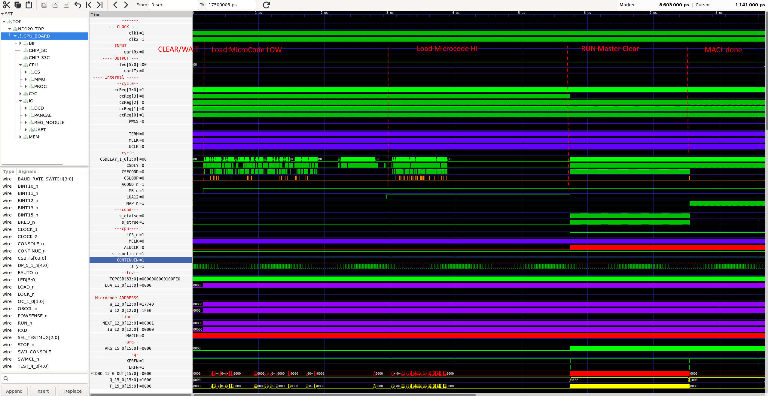
Verilator compiles and runs the full boot path: microcode load, "Master Clear",
then the MACL CPU self-test (passes clean - 0 STERR visits, measured 13-JUL
with the runSim ND120_COUNT_STERR probe; the old "7 of 14" figure predated the
07-JUL transparent-latch fix), after which OPCOM UART communication works (use
the runSim/ harness to interact with it).
SINTRAN III boots on FPGA silicon: Tang Nano 20K (24-AUG-2026, the
ND3202D.v:533 bus bank-decode fix in HISTORY.md), Nexys 4 DDR (25-AUG-2026)
and MiSTer / DE10-Nano (02-SEP-2026). The Basys3 boots OPCOM only; the MEGA65
cores and the QMTECH bitstream are built and timing-clean but have not run on
their boards. Per-board state, clocks and limits: fpga/README.md.
| Folder | Source | Comment |
|---|---|---|
| DELILAH-CPU | Logisim drawing complete | CGA |
| DECODE-GateArray | Logisim drawing complete | DGA |
| CPU-BOARD-3202 | Logisim drawing complete | Support chips TTL/MEMORY/++ |
| PAL | No Logisim, PALASM source | Hand converted PALASM to Verilog for all PALs |
| Shared | Shared code between the CPU, DGA and 3202D CPU board. Mix of converted Logisim and hand-written modules |
The Verilog is no longer generated from Logisim; both are kept by hand (see
../DEVELOPMENT.md, "Source of truth").
Reference documents
tests/README.md— whatmake testruns, measured coverage, and the orphan gateOWNERSHIP.md— who may edit what, and the hard rules around builds, boards and gitdocs/SIGNALS.md— what each control signal is, who drives it, and how that was establisheddocs/RETRACTED.md— claims this repo once asserted that turned out to be wrongPAL/PROVENANCE.md— how a PAL is proved faithful to its PALASM listing../DesignDocuments/PAL-Code/— the PALASM listings (SRC/), the scans (IMG/, authoritative), and the 2026 transcription audit
Testbench conventions
Testbenches live in a sim/ subdirectory next to the module source code:
<component>/
  circuit/
    module.v              ← source
  sim/
    Makefile              ← build & run targets
    module_tb.v           ← iverilog testbench
    test_module.cpp       ← Verilator testbench (if applicable)
    *.gtkw                ← GTKWave waveform configs
    README.md             ← test documentation
This keeps the test next to what it tests — no searching. Examples:
DELILAH-CPU/CGA_MIC/sim/MASEL_cycle_tb.vtestsDELILAH-CPU/CGA_MIC/circuit/CGA_MIC_MASEL.vCPU-BOARD-3202/circuit/CPU_CS_ACAL_17/sim/testsCPU_CS_ACAL_17.v
Testbench types:
| Tool | File pattern | Use case |
|---|---|---|
| iverilog | *_tb.v |
Fast unit tests, race-condition validation, timing checks |
| Verilator | test_*.cpp |
Full-module simulation with C++ harness, waveform generation |
Running testbenches:
# From WSL, cd to the module's sim/ directory
cd Verilog/DELILAH-CPU/CGA_MIC/sim

# iverilog testbenches
make test-masel          # run all MASEL tests
make test-masel-cycle    # run cycle/race testbench only

# Verilator full-module test
make all                 # compile, run, open GTKWave
Legacy:
tests/vivado_warning_fixes/contains older testbenches from the initial Vivado warning fix pass. New testbenches should go in the module'ssim/directory following the convention above.
Run Verilog code using Verilator
There are two top-level Verilator harnesses. They build the same
ND120_TOP module but serve opposite purposes — one is a hands-off waveform
logger, the other is a live interactive console. Pick by what you need to do:
| Folder | Mode | Driven by | UART / OPCOM | Stops when | Use it to… |
|---|---|---|---|---|---|
sim/ |
Automatic (batch) | test_nd120.cpp |
Scripted — canned commands auto-answer the CPU prompts | after a fixed tick budget | Capture FST waveforms for GTKWave and run latch-vs-FF regression |
runSim/ |
Interactive (manual) | Run120.cpp |
Live — your keyboard is wired to the CPU serial line | you press Ctrl+C | Talk to the running CPU: drive OPCOM, type commands, watch output |
sim/ — automatic waveform logger (no keyboard input)
Boots a BPUN tape into simulated RAM, steps the clock for a fixed number of
ticks, and writes waveform.fst. The serial "conversation" is pre-scripted:
a bit-banged UART model watches the CPU's output and replies with hardcoded
commands — you see OPCOM output echoed to the terminal but cannot type to
it (stdin reading is intentionally disabled). This is the harness for
signal-level debugging and for proving a refactor didn't change behaviour.
cd Verilog/sim
make clean
make all            # compile + run + open GTKWave (waveform.fst + top_3202d.gtkw)
make test_nd120     # compile only
make run            # run only (produces waveform.fst)
make gtk            # open GTKWave on the last run

# Latch-vs-FF regression: build both modes, run each, diff the traces
make compare        # -> trace_latch.csv vs trace_ff.csv -> trace_diff.txt
                    #    prints "IDENTICAL" or "DIVERGENCE FOUND"
runSim/ — interactive console (manual testing)
The one to use when you want to operate the CPU by hand. It puts your
terminal into raw, non-blocking mode, reads live keystrokes, and serializes
them onto the CPU's UART RX pin; CPU UART output is printed straight back to
the screen. It runs the microcode load + self-test and then drops you into the
program's interactive mode (OPCOM operator communication) over that serial
link. The loop runs indefinitely until you press Ctrl+C. Defaults to
loading DEBUG.BPUN; pass a different tape as the first argument.
cd Verilog/runSim
make clean
make compile
make run                                # loads DEBUG.BPUN, gives you the console
./obj_dir/VND120_TOP INSTRUCTION-B.BPUN # run a different program tape
Both harnesses honour
USE_LATCHES(default1= original transparent-latch behaviour;0adds-DFPGA_FF_MODEfor edge-triggered FPGA-style flip-flops) and always compile with-DVERILATOR_SIM(enables the bus ports, fast UART, and large simulation RAM — see RAM configuration below).
RAM Configuration for Verilator vs FPGA
MEM_RAM_49.v (sheet 49, the on-board RAM) picks its size from compile-time
defines. No manual changes needed.
- Verilator simulation: 6 x 1M words (
RAM_SIZE=2), enabled by-DVERILATOR_SIM(already set insim/MakefileandrunSim/Makefile).-DND120_SIM_RAM_64Kgives 64K words per chip for faster TPE runs. - FPGA builds that keep main memory in block RAM (Basys3, Cmod A7): the
small setting (
RAM_SIZE=3, 24 KB). Thexc7a35thas only 100 RAMB18 blocks; 6 MB would need 3496 of them (35x the device). Enough for the CPU logic and small test programs, never for SINTRAN. - Boards with external memory (Tang Nano 20K SDRAM, Nexys 4 DDR DDR2, MiSTer and MEGA65 R4-R6 SDRAM, MEGA65 R3 HyperRAM, QMTECH SDRAM) replace the block-RAM sheet with a memory backend and give the CPU 4 MB or more - see each board's README.
Devices, addresses and disc geometry
docs/device-address-map.md- every ND-BUS device: octal IOX base, ident code, interrupt level, module and backing image, plus the boot/mass-load console commands.ND-BUS-DEVICES/README.md- the bus handshake, IDENT cascade rules, and the Winchester vs SMD disc geometry table (they are nearly the same size with different geometries; mixing them up corrupts transfers silently).SD-FAT/CARD-LAYOUT.md- what the SD card must look like: root directory only, 8.3 names, length-exact matching.
Supported hardware targets
The same HDL source builds for the Verilator simulator and for every FPGA board
under fpga/, one folder per board - only board-specific
build scripts, constraints and tool projects are per-target. The board list,
status, clocks and measured limits live in fpga/README.md
and are not repeated here.
Verilator (simulation — the working reference)
No hardware needed; this is the golden reference every FPGA build is compared against. Two harnesses, described in detail above:
# Waveform / signal-level sim (FST + GTKWave)
cd Verilog/sim && make clean && make all

# Interactive full-CPU sim (microcode load + self-test + live OPCOM console)
cd Verilog/runSim && make clean && make compile && make run
Basys3 — synthesize & deploy (Vivado, Windows host)
The Vivado project lives outside the repository (its location is set in the build script). Run from Windows PowerShell:
cd Verilog/fpga/basys3

# Synthesize + implement + write bitstream (~1h full synth; copies microcode hex first)
.\vivado_build.ps1
#   -> output\ND120_TOP.bit in the Vivado project (+ .ltx for ILA probes)

# Deploy to the board:
.\flash.ps1 -Quick     # JTAG only (volatile) - fast iteration
.\flash.ps1            # JTAG + SPI flash - survives power cycle
vivado_build.tcl flags: full_synth, skip_program, no_reset_synth,
backup_bit; vivado_lint.tcl runs lint only. The microcode hex files
AM27256_4513{2,3}L.hex must be in the project dir (the .ps1 copies them from
Code/Microcode/) or the ROM is empty. Details:
fpga/basys3/README.md. The Nexys 4 DDR has its own
build script (fpga/nexys4ddr/build.tcl, see its README).
Tang Nano 20K — synthesize & deploy (Gowin)
Two flows (details in
fpga/tang-nano-20k/README.md):
-
OSS flow (Linux/WSL, no Windows round-trip) - marked PRIMARY in
fpga/tang-nano-20k/Makefile:source ~/oss-cad-suite/environment # install: see fpga/tang-nano-20k/README.md cd Verilog/fpga/tang-nano-20k && make # yosys synth_gowin -> nextpnr-himbaechel -> gowin_pack openFPGALoader -b tangnano20k <bitstream>.fs # SRAM (volatile) openFPGALoader -b tangnano20k -f <bitstream>.fs # config flash (persistent)
-
Gowin EDA:
fpga/tang-nano-20k/gowin_build.ps1 -Variant <slow|crawl|mid|full|fast20>. Thefast20variant (20.25 MHz, timing-clean) is the one that boots SINTRAN with a 115200 console; it exists only in this flow.Pin constraints:
fpga/tang-nano-20k/src/nd120_tang20k.cst. Board hardware reference: Sipeed wiki - Tang Nano 20K. The 8 MB embedded SDRAM has a standalone bring-up test (nand2mario controller + ND-120 UART at 9600 baud) infpga/tang-nano-20k/sdram-test/- buildable with both Gowin EDA (sdram_test.gprj) and the OSS flow (make), with a passing iverilog testbench (make sim). Verified on hardware 2026-07-08: OSS-flow bitstream, 1 MB write+verify passes; that README also documents the usbipd/WSL2 program-and-console workflow.
Key shared facts:
- One clock. FPGA builds run every flip-flop on
sysclkwith clock-enables instead of clocking on derived signals. How board behaviour is compared against Verilator:docs/fpga-debug-methodology.mdandsim/FPGA_DEBUG_RUNBOOK.md. - Microcode preload:
SKIP_WCS_LOADbitstream-preloads the WCS and skips the runtime load phase (verified in Verilator; required to fit the Tang's BSRAM). Details:docs/skip-wcs-load.md. - All build options — Verilog defines, sim make variables, Vivado/Gowin
build flags per board, and the runSim runtime probe env vars — in one
reference:
docs/build-defines.md. - Expected boot sequence for validation:
docs/boot-golden-spec.md. - Open work:
TODO.md. - All design docs, handoffs, and plans are indexed in
docs/README.md; the ND-100 bus protocol (IOX / IDENT / DMA) is written up indocs/nd100-bus-dma.mdwith a slide deck atdocs/nd100-bus-deck.pptx.
CPU Boot process
- Some delay to reset all components
- Loads Microcode first 32KB (low)
- Loads Microcode next 32KB (high)
- Starts at microcode address 0 (Master Clear/Power Clear)
- Jumps to MACL
- Clears/Initializes internal registers and sets up UART
- Runs self-test program for CPU, Test 1-8
- Depending on the input from the PANEL keylock it will either try to automatic load code from storage depending on ALD settings
-
- or go to OPCOM mode where one can communicate with the CPU via UART
Test program verification