basys3_mem_test_top
Source: Verilog/fpga/basys3/mem-test/basys3_mem_test_top.v
Hierarchy: not instantiated by any of the 9 build tops (elaborated by yosys).
Module hierarchy - All modules
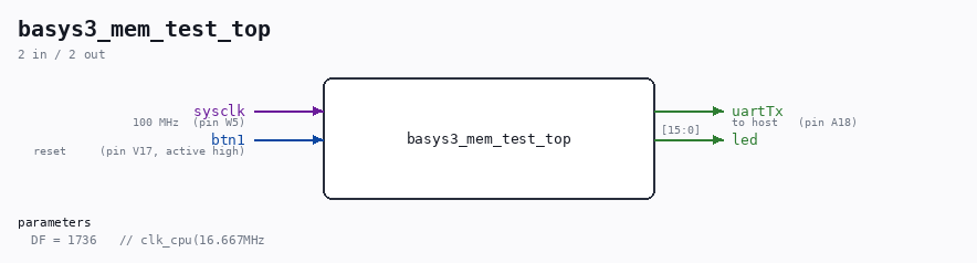
Schematic
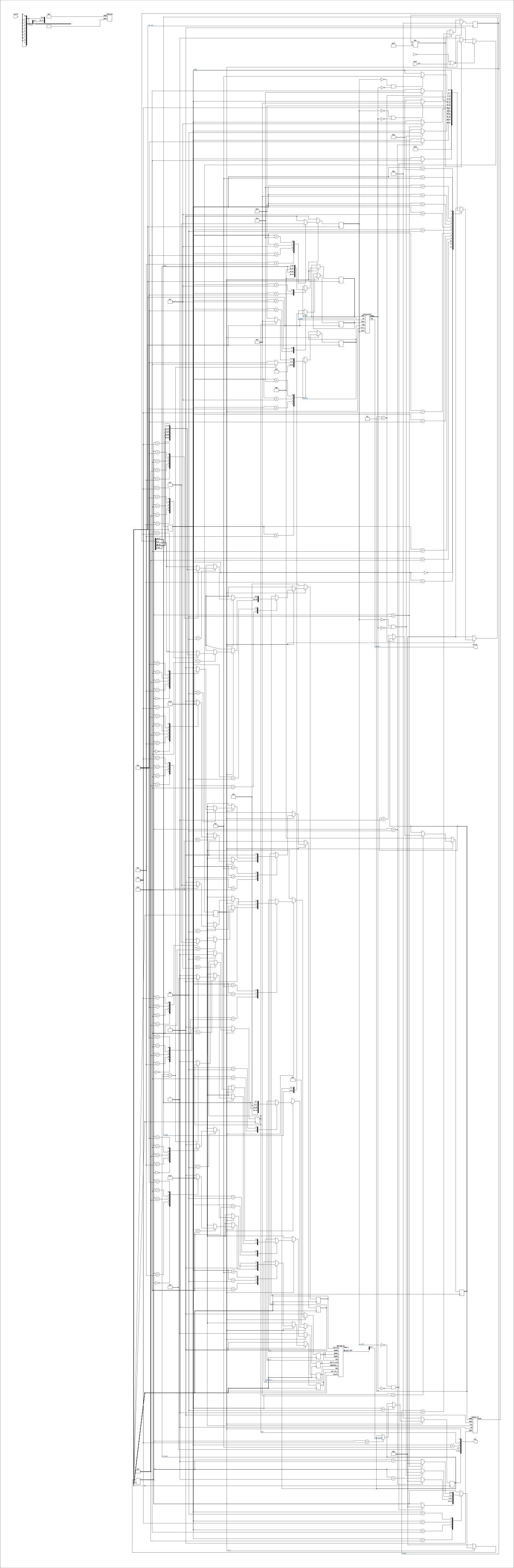
Drawn from the Verilog: no build top uses this module, so it was elaborated from its own file with no defines and default parameters. Sub-modules are boxes (click the picture to open it full size; there every sub-module box links to its page, and every wire shows its Verilog name).
Description
Basys3 standalone memory test for the ND-120 BRAM path Isolates MEM_RAM_49 (-> SIP1M9 sync BRAM, ramSize=3) from the whole CPU. Drives the exact DRAM RAS/CAS/AA protocol the real controller uses (captured via DBG_MEM: row valid at RAS-fall, AA -> col while CAS still high, both strobes low a few cycles, read data captured while RAS is deasserted and CAS still low), then writes+reads+verifies a handful of addresses and reports each over UART (9600 8N1) using msg_printer. If this PASSES on the board, the BRAM path is fine and the memory bug is in the CPU/MAC integration. If it FAILS, the fault is here where we can iterate directly.
Parameters
| Parameter | Default |
|---|---|
DF |
1736 // clk_cpu(16.667MHz |
Ports
| Direction | Width | Name | Description |
|---|---|---|---|
| input | 1 |
sysclk |
100 MHz (pin W5) |
| input | 1 |
btn1 |
reset (pin V17, active high) |
| output | 1 |
uartTx |
to host (pin A18) |
| output | [15:0] |
led |
Verilog source
Verilog/fpga/basys3/mem-test/basys3_mem_test_top.v on GitHub.
Show the Verilog of basys3_mem_test_top (179 lines)
/****************************************************************************
** Basys3 standalone memory test for the ND-120 BRAM path                   **
**                                                                          **
** Isolates MEM_RAM_49 (-> SIP1M9 sync BRAM, ramSize=3) from the whole CPU. **
** Drives the exact DRAM RAS/CAS/AA protocol the real controller uses        **
** (captured via DBG_MEM: row valid at RAS-fall, AA -> col while CAS still   **
** high, both strobes low a few cycles, read data captured while RAS is      **
** deasserted and CAS still low), then writes+reads+verifies a handful of    **
** addresses and reports each over UART (9600 8N1) using msg_printer.        **
**                                                                          **
** If this PASSES on the board, the BRAM path is fine and the memory bug is  **
** in the CPU/MAC integration. If it FAILS, the fault is here where we can    **
** iterate directly.                                                         **
****************************************************************************/
`default_nettype none

module basys3_mem_test_top #(
    parameter integer DF = 1736   // clk_cpu(16.667MHz)/9600; override small for sim
) (
    input  wire        sysclk,   // 100 MHz  (pin W5)
    input  wire        btn1,     // reset     (pin V17, active high)
    output wire        uartTx,   // to host   (pin A18)
    output wire [15:0] led
);

`ifdef NO_MMCM
  // Simulation: drive clk_cpu directly from the input clock (no Xilinx primitive)
  wire clk_cpu     = sysclk;
  wire mmcm_locked = 1'b1;
`else
  // ---------- 100 MHz -> 16.667 MHz clk_cpu (same MMCM as ND120_TOP) ----------
  wire clk_cpu, clk_cpu_pre, clkfb_out, clkfb_in, mmcm_locked;
  MMCME2_BASE #(
      .BANDWIDTH("OPTIMIZED"), .CLKFBOUT_MULT_F(10.0), .CLKIN1_PERIOD(10.0),
      .CLKOUT0_DIVIDE_F(60.0), .DIVCLK_DIVIDE(1), .STARTUP_WAIT("FALSE")
  ) mmcm (
      .CLKIN1(sysclk), .CLKFBIN(clkfb_in), .CLKFBOUT(clkfb_out),
      .CLKOUT0(clk_cpu_pre), .LOCKED(mmcm_locked), .PWRDWN(1'b0), .RST(1'b0)
  );
  BUFG bfb (.I(clkfb_out),   .O(clkfb_in));
  BUFG bcp (.I(clk_cpu_pre), .O(clk_cpu));
`endif

  // ---------- reset ----------
  reg [7:0] rstcnt = 8'h00;
  reg       rst_n  = 1'b0;
  always @(posedge clk_cpu) begin
    if (!mmcm_locked || btn1) begin rstcnt <= 0; rst_n <= 1'b0; end
    else if (rstcnt != 8'hFF)     rstcnt <= rstcnt + 1'b1;
    else                          rst_n <= 1'b1;
  end

  // DF (baud divisor) is a module parameter (default 1736 = 16.667 MHz / 9600)

  // ---------- MEM_RAM_49 (ramSize=3 -> sync BRAM) ----------
  reg  [9:0]  aa;
  reg         ras, cas, bank0, mwrite_n;
  reg  [17:0] dd_in;
  wire [17:0] dd_out;
  wire        corr_n;
  MEM_RAM_49 ram (
      .sysclk(clk_cpu), .sys_rst_n(rst_n),
      .AA_9_0(aa), .BANK0(bank0), .BANK1(1'b0), .BANK2(1'b0),
      .CAS(cas), .RAS(ras), .MWRITE50_n(mwrite_n),
      .DD_17_0_IN(dd_in), .DD_17_0_OUT(dd_out), .CORR_n(corr_n)
  );

  // ---------- test vectors (addr, data) ----------
  reg  [19:0] t_addr;
  reg  [7:0]  t_data;
  reg  [2:0]  tidx;
  always @(*) begin
    case (tidx)
      3'd0: begin t_addr = 20'h00000; t_data = 8'hA5; end
      3'd1: begin t_addr = 20'h00001; t_data = 8'h5A; end
      3'd2: begin t_addr = 20'h00002; t_data = 8'h3C; end
      3'd3: begin t_addr = 20'h00004; t_data = 8'hC3; end  // old model aliased 0<->4
      3'd4: begin t_addr = 20'h00010; t_data = 8'hFF; end
      3'd5: begin t_addr = 20'h00100; t_data = 8'h11; end
      3'd6: begin t_addr = 20'h000FF; t_data = 8'h77; end
      3'd7: begin t_addr = 20'h003FF; t_data = 8'h42; end
    endcase
  end
  wire [9:0] row = t_addr[9:0];
  wire [9:0] col = t_addr[19:10];

  // ---------- msg_printer ----------
  reg         p_start;
  reg  [3:0]  p_msg;
  reg  [22:0] p_addr;
  reg  [7:0]  p_data;
  wire        p_busy;
  msg_printer #(.DELAY_FRAMES(DF)) printer (
      .clk(clk_cpu), .rst_n(rst_n), .start(p_start), .msg(p_msg),
      .addr(p_addr), .data(p_data), .busy(p_busy), .txd(uartTx)
  );
  // msg selectors (must match msg_printer.v)
  localparam M_BANNER=4'd0, M_WRITE=4'd2, M_READ_OK=4'd3, M_READ_ERR=4'd4,
             M_PASS=4'd8, M_FAIL=4'd9;

  // ---------- main FSM ----------
  localparam S_RST=0, S_BANNER=1, S_BANWAIT=2,
             S_WR=3, S_WRMSG=4, S_WRMSGW=5,
             S_RD=6, S_RDMSG=7, S_RDMSGW=8,
             S_NEXT=9, S_RESULT=10, S_RESWAIT=11, S_DONE=12;
  reg [3:0] state;
  reg [3:0] d;         // DRAM sub-cycle 0..6
  reg [7:0] rd_data;
  reg       fail;

  // DRAM protocol driven by sub-cycle d (each = 1 clk_cpu), is_write = (state==S_WR)
  task drive_dram(input is_write);
    begin
      // defaults (idle)
      ras=1'b0; cas=1'b0; bank0=1'b0; mwrite_n=1'b1;
      aa=row; dd_in={10'b0, t_data};
      case (d)
        4'd0: begin ras=1; bank0=1; aa=row; mwrite_n=~is_write ? 1'b1 : 1'b0; end // RAS fall, row
        4'd1: begin ras=1; bank0=1; aa=col; mwrite_n= is_write?1'b0:1'b1; end     // AA->col, CAS high
        4'd2: begin ras=1; bank0=1; cas=1; aa=col; mwrite_n=is_write?1'b0:1'b1; end// CAS fall, col
        4'd3: begin ras=1; bank0=1; cas=1; aa=col; mwrite_n=is_write?1'b0:1'b1; end// both low
        4'd4: begin ras=1; bank0=1; cas=1; aa=col; mwrite_n=is_write?1'b0:1'b1; end// both low
        4'd5: begin ras=0; bank0=1; cas=1; aa=col; mwrite_n=1'b1; end             // RAS deassert, read window
        default: begin ras=0; cas=0; bank0=0; end                                // precharge
      endcase
    end
  endtask

  always @(posedge clk_cpu) begin
    if (!rst_n) begin
      state<=S_RST; d<=0; tidx<=0; fail<=0; p_start<=0;
      ras<=0; cas<=0; bank0<=0; mwrite_n<=1; aa<=0; dd_in<=0; rd_data<=0;
    end else begin
      p_start <= 1'b0;
      case (state)
        S_RST: begin state<=S_BANNER; end
        S_BANNER: begin p_msg<=M_BANNER; p_start<=1; state<=S_BANWAIT; end
        S_BANWAIT: if (!p_start && !p_busy) begin d<=0; state<=S_WR; end

        // ---- write access ----
        S_WR: begin
          drive_dram(1'b1);
          if (d==4'd6) begin d<=0; state<=S_WRMSG; end else d<=d+1'b1;
        end
        S_WRMSG: begin p_msg<=M_WRITE; p_addr<={3'b0,t_addr}; p_data<=t_data; p_start<=1; state<=S_WRMSGW; end
        S_WRMSGW: if (!p_start && !p_busy) begin d<=0; state<=S_RD; end

        // ---- read access ----
        S_RD: begin
          drive_dram(1'b0);
          if (d==4'd5) rd_data<=dd_out[7:0];       // capture in the read window
          if (d==4'd6) begin d<=0; state<=S_RDMSG; end else d<=d+1'b1;
        end
        S_RDMSG: begin
          p_addr<={3'b0,t_addr}; p_data<=rd_data;
          if (rd_data==t_data) p_msg<=M_READ_OK;
          else begin p_msg<=M_READ_ERR; fail<=1'b1; end
          p_start<=1; state<=S_RDMSGW;
        end
        S_RDMSGW: if (!p_start && !p_busy) state<=S_NEXT;

        S_NEXT: if (tidx==3'd7) state<=S_RESULT; else begin tidx<=tidx+1'b1; state<=S_WR; end
        S_RESULT: begin p_msg<= fail ? M_FAIL : M_PASS; p_start<=1; state<=S_RESWAIT; end
        S_RESWAIT: if (!p_start && !p_busy) state<=S_DONE;
        S_DONE: begin ras<=0; cas<=0; bank0<=0; end
        default: state<=S_RST;
      endcase
    end
  end

  assign led[0]    = rst_n;
  assign led[1]    = fail;
  assign led[2]    = (state==S_DONE);
  assign led[7:3]  = 5'b0;
  assign led[15:8] = rd_data;   // last read byte, for a quick visual

endmodule

`default_nettype wire