emu
Source: Verilog/fpga/mister/nd120.sv
Where it sits (MiSTer): emu
Used in: nothing - this is a top (MiSTer).
Contains: console_uart_rx, console_uart_tx, hps_io (vendor), mips_counter, nd120_console_mister, ND120_CORE, nd_storage_mister_devices, pll (vendor), pll_cpu
Module hierarchy - All modules
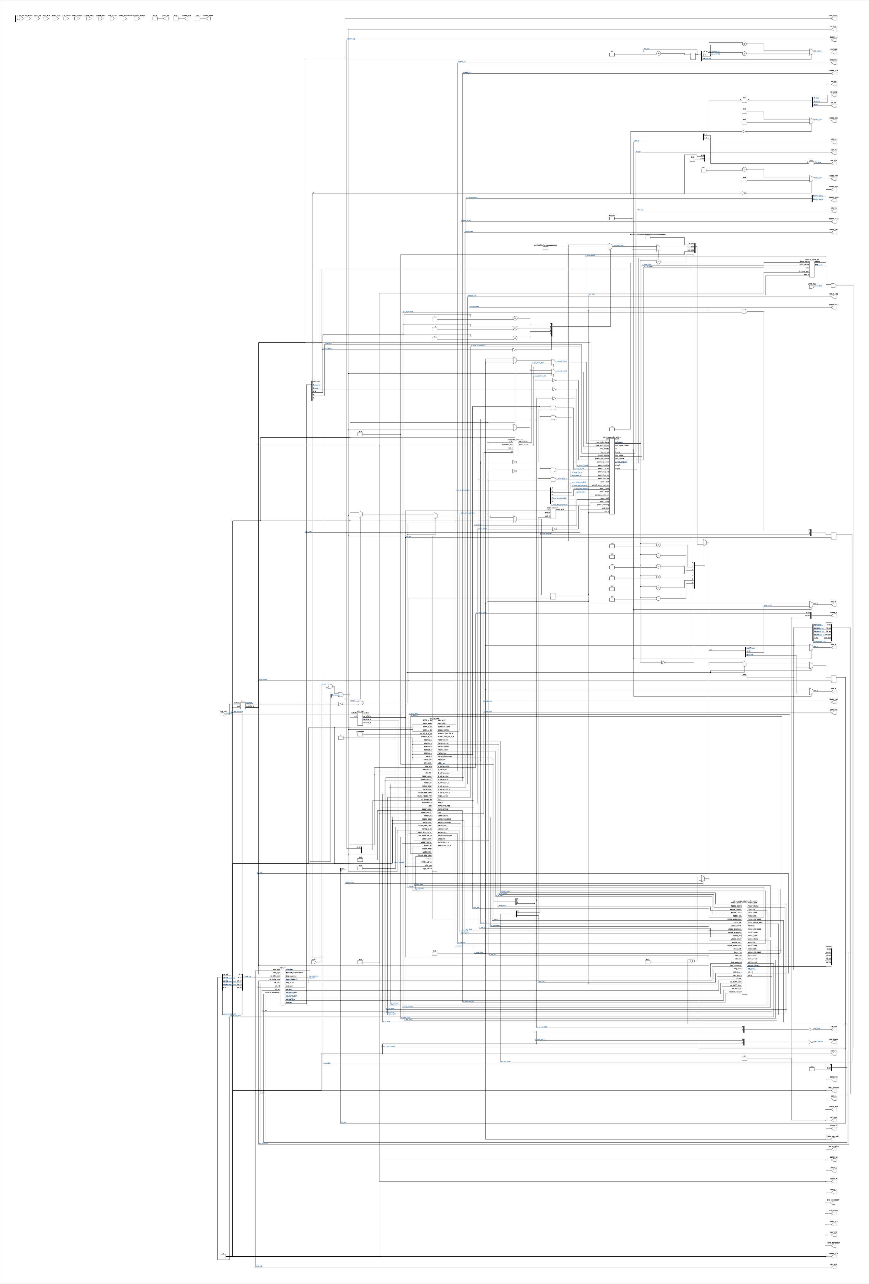
Schematic
Drawn from the Verilog: the yosys netlist of the MiSTer build, where it is the top. Sub-modules are boxes (click the picture to open it full size; there every sub-module box links to its page, and every wire shows its Verilog name).
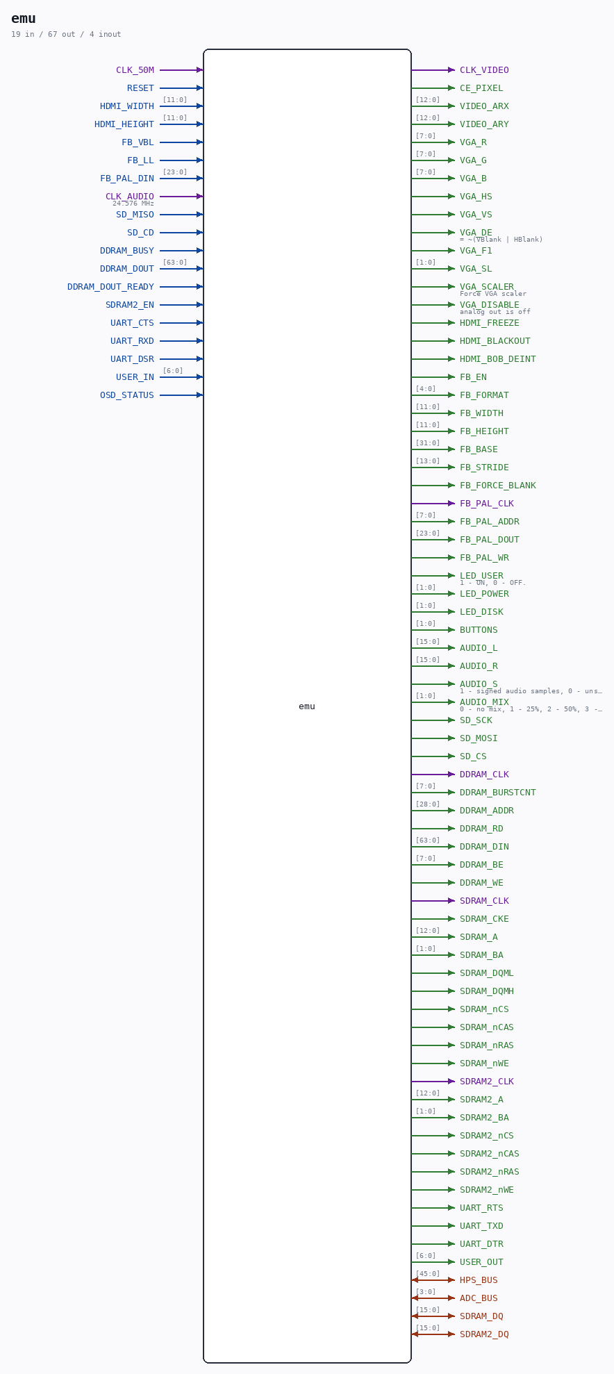
Ports
| Direction | Width | Name | Description |
|---|---|---|---|
| input | 1 |
CLK_50M |
|
| input | 1 |
RESET |
|
| inout | [45:0] |
HPS_BUS |
|
| output | 1 |
CLK_VIDEO |
|
| output | 1 |
CE_PIXEL |
|
| output | [12:0] |
VIDEO_ARX |
|
| output | [12:0] |
VIDEO_ARY |
|
| output | [7:0] |
VGA_R |
|
| output | [7:0] |
VGA_G |
|
| output | [7:0] |
VGA_B |
|
| output | 1 |
VGA_HS |
|
| output | 1 |
VGA_VS |
|
| output | 1 |
VGA_DE |
= ~(VBlank | HBlank) |
| output | 1 |
VGA_F1 |
|
| output | [1:0] |
VGA_SL |
|
| output | 1 |
VGA_SCALER |
Force VGA scaler |
| output | 1 |
VGA_DISABLE |
analog out is off |
| input | [11:0] |
HDMI_WIDTH |
|
| input | [11:0] |
HDMI_HEIGHT |
|
| output | 1 |
HDMI_FREEZE |
|
| output | 1 |
HDMI_BLACKOUT |
|
| output | 1 |
HDMI_BOB_DEINT |
|
| output | 1 |
FB_EN |
|
| output | [4:0] |
FB_FORMAT |
|
| output | [11:0] |
FB_WIDTH |
|
| output | [11:0] |
FB_HEIGHT |
|
| output | [31:0] |
FB_BASE |
|
| output | [13:0] |
FB_STRIDE |
|
| input | 1 |
FB_VBL |
|
| input | 1 |
FB_LL |
|
| output | 1 |
FB_FORCE_BLANK |
|
| output | 1 |
FB_PAL_CLK |
|
| output | [7:0] |
FB_PAL_ADDR |
|
| output | [23:0] |
FB_PAL_DOUT |
|
| input | [23:0] |
FB_PAL_DIN |
|
| output | 1 |
FB_PAL_WR |
|
| output | 1 |
LED_USER |
1 - ON, 0 - OFF. |
| output | [1:0] |
LED_POWER |
|
| output | [1:0] |
LED_DISK |
|
| output | [1:0] |
BUTTONS |
|
| input | 1 |
CLK_AUDIO |
24.576 MHz |
| output | [15:0] |
AUDIO_L |
|
| output | [15:0] |
AUDIO_R |
|
| output | 1 |
AUDIO_S |
1 - signed audio samples, 0 - unsigned |
| output | [1:0] |
AUDIO_MIX |
0 - no mix, 1 - 25%, 2 - 50%, 3 - 100% (mono) |
| inout | [3:0] |
ADC_BUS |
|
| output | 1 |
SD_SCK |
|
| output | 1 |
SD_MOSI |
|
| input | 1 |
SD_MISO |
|
| output | 1 |
SD_CS |
|
| input | 1 |
SD_CD |
|
| output | 1 |
DDRAM_CLK |
|
| input | 1 |
DDRAM_BUSY |
|
| output | [7:0] |
DDRAM_BURSTCNT |
|
| output | [28:0] |
DDRAM_ADDR |
|
| input | [63:0] |
DDRAM_DOUT |
|
| input | 1 |
DDRAM_DOUT_READY |
|
| output | 1 |
DDRAM_RD |
|
| output | [63:0] |
DDRAM_DIN |
|
| output | [7:0] |
DDRAM_BE |
|
| output | 1 |
DDRAM_WE |
|
| output | 1 |
SDRAM_CLK |
|
| output | 1 |
SDRAM_CKE |
|
| output | [12:0] |
SDRAM_A |
|
| output | [1:0] |
SDRAM_BA |
|
| inout | [15:0] |
SDRAM_DQ |
|
| output | 1 |
SDRAM_DQML |
|
| output | 1 |
SDRAM_DQMH |
|
| output | 1 |
SDRAM_nCS |
|
| output | 1 |
SDRAM_nCAS |
|
| output | 1 |
SDRAM_nRAS |
|
| output | 1 |
SDRAM_nWE |
|
| input | 1 |
SDRAM2_EN |
|
| output | 1 |
SDRAM2_CLK |
|
| output | [12:0] |
SDRAM2_A |
|
| output | [1:0] |
SDRAM2_BA |
|
| inout | [15:0] |
SDRAM2_DQ |
|
| output | 1 |
SDRAM2_nCS |
|
| output | 1 |
SDRAM2_nCAS |
|
| output | 1 |
SDRAM2_nRAS |
|
| output | 1 |
SDRAM2_nWE |
|
| input | 1 |
UART_CTS |
|
| output | 1 |
UART_RTS |
|
| input | 1 |
UART_RXD |
|
| output | 1 |
UART_TXD |
|
| output | 1 |
UART_DTR |
|
| input | 1 |
UART_DSR |
|
| input | [6:0] |
USER_IN |
|
| output | [6:0] |
USER_OUT |
|
| input | 1 |
OSD_STATUS |
Verilog source
Verilog/fpga/mister/nd120.sv on GitHub.
Show the Verilog of emu (1087 lines)
//============================================================================
//
//  This program is free software; you can redistribute it and/or modify it
//  under the terms of the GNU General Public License as published by the Free
//  Software Foundation; either version 2 of the License, or (at your option)
//  any later version.
//
//  This program is distributed in the hope that it will be useful, but WITHOUT
//  ANY WARRANTY; without even the implied warranty of MERCHANTABILITY or
//  FITNESS FOR A PARTICULAR PURPOSE.  See the GNU General Public License for
//  more details.
//
//  You should have received a copy of the GNU General Public License along
//  with this program; if not, write to the Free Software Foundation, Inc.,
//  51 Franklin Street, Fifth Floor, Boston, MA 02110-1301 USA.
//
//============================================================================

module emu
(
    `include "sys/emu_ports.vh"
);

///////// Default values for ports not used in this core /////////

assign ADC_BUS  = 'Z;
assign USER_OUT = '1;
// UART_TXD is driven from the CPU's console further down - see "SERIAL
// CONSOLE". RTS/DTR stay inactive; the ND-120 console is 3-wire.
assign {UART_RTS, UART_DTR} = 0;
assign {SD_SCK, SD_MOSI, SD_CS} = 'Z;
// SDRAM: main memory (01-SEP-2026) - driven by the sheet-49 SDRAM bridge
// through ND120_CORE, see the CLOCKS and MAIN MEMORY notes below.
assign {DDRAM_CLK, DDRAM_BURSTCNT, DDRAM_ADDR, DDRAM_DIN, DDRAM_BE, DDRAM_RD, DDRAM_WE} = '0;

assign VGA_SL = 0;
assign VGA_F1 = 0;
assign VGA_SCALER  = 0;
assign VGA_DISABLE = 0;
assign HDMI_FREEZE = 0;
assign HDMI_BLACKOUT = 0;
assign HDMI_BOB_DEINT = 0;

assign AUDIO_S = 0;
assign AUDIO_L = 0;
assign AUDIO_R = 0;
assign AUDIO_MIX = 0;

// LED_DISK / LED_POWER are driven from the CPU's own status lamps further
// down, once s_core_led is declared - see "CPU status lamps".
assign BUTTONS = 0;

//////////////////////////////////////////////////////////////////

wire [1:0] ar = status[122:121];

assign VIDEO_ARX = (!ar) ? 12'd4 : (ar - 1'd1);
assign VIDEO_ARY = (!ar) ? 12'd3 : 12'd0;

`include "build_id.v"
localparam CONF_STR = {
    "ND120;;",
    "-;",
    "O[122:121],Aspect ratio,Original,Full Screen,[ARC1],[ARC2];",
    "-;",
    "O[6],Keyboard,US,Norwegian;",
    // Panel default ON (build 2, 31-AUG-2026): status bits reset to 0, so
    // bit 0 = "On" and bit 1 = "Off" gives default-on with no extra default-
    // value machinery. Same DBG_PANEL signals the Nexys build's sw[3] shows.
    "O[7],Operator panel,On,Off;",
    // Console font colour (02-SEP-2026). The terminal core emits a palette
    // INDEX; this only re-tints the console-text index in the RGB map below,
    // so it is a board-only cosmetic - the panel colours and the terminal RTL
    // are untouched. Default Green (the green Tandberg look the ND grew up
    // with). status[9:8], freed when the baud selector was removed.
    "O[9:8],Console colour,Green,Amber,White,Cyan;",
    "-;",
    // Disk and tape images (01-SEP-2026, PLAN-mister-storage.md). One OSD
    // mount slot per drive, served through hps_io's block interface by
    // rtl/nd_storage_hps.v - the pattern the mainstream MiSTer computer
    // cores use (Atari ST, Apple II, C64, BK0011M, TRS-80...). The slot
    // number IS the hps_io index IS the storage client: see the slot map in
    // rtl/nd_storage_mister_devices.v. Slot 4 is outside the documented 0-3
    // range but inside what the code accepts (hps_io VDNUM 1..10) and is
    // what TRS-80_MiSTer ships; it carries the tape so the four disc slots
    // stay in the documented range. Extensions are 3-character groups; a
    // 4-letter ".BPUN" cannot be named, so tapes are ".BPU" or ".TAP" here.
    // The HPS automounts boot0.vhd..boot3.vhd / ND120.VHD from the core's
    // folder into slots 0-3 at start - never ship such files.
    "S0,IMG,Floppy drive 0;",
    "S1,IMG,Floppy drive 1;",
    "S2,IMG,Winchester unit 0;",
    "S3,IMG,Winchester unit 1;",
    "S4,BPUTAP,Paper tape;",
    "-;",
    "T[0],Reset;",
    "R[0],Reset and close OSD;",
    "v,0;",
    "V,v",`BUILD_DATE
};

wire forced_scandoubler;
wire   [1:0] buttons;
wire [127:0] status;
wire  [10:0] ps2_key;

// ---- the block interface to the mounted images (clk_sys) -----------------
// VDNUM 5 = the five S slots above. BLKSZ 2 = 512-byte HPS blocks; the
// storage backend asks for four at a time (sd_blk_cnt = 3) so one ND-120
// storage block (2048 bytes) is one HPS transaction. WIDE = 16-bit words on
// the buffer bus. The ND side of this is plain Verilog with flattened
// per-slot vectors; the unpacking into hps_io's arrays is right here.
localparam VDNUM = 5;
wire [VDNUM-1:0] img_mounted;
wire             img_readonly;
wire      [63:0] img_size;
wire      [31:0] sd_lba[VDNUM];
wire       [5:0] sd_blk_cnt[VDNUM];
wire [VDNUM-1:0] sd_rd, sd_wr, sd_ack;
wire      [12:0] sd_buff_addr;
wire      [15:0] sd_buff_dout;
wire      [15:0] sd_buff_din[VDNUM];
wire             sd_buff_wr;
wire [VDNUM*32-1:0] sd_lba_flat;
wire [VDNUM*6-1:0]  sd_blk_cnt_flat;
wire      [15:0] sd_buff_din_one;   // one transaction in flight: same word to every slot
genvar vd;
generate
    for (vd = 0; vd < VDNUM; vd = vd + 1) begin : g_vd
        assign sd_lba[vd]      = sd_lba_flat[vd*32 +: 32];
        assign sd_blk_cnt[vd]  = sd_blk_cnt_flat[vd*6 +: 6];
        assign sd_buff_din[vd] = sd_buff_din_one;
    end
endgenerate

hps_io #(.CONF_STR(CONF_STR), .VDNUM(VDNUM), .BLKSZ(2), .WIDE(1)) hps_io
(
    .clk_sys(clk_sys),
    .HPS_BUS(HPS_BUS),
    .EXT_BUS(),
    .gamma_bus(),

    .forced_scandoubler(forced_scandoubler),

    .buttons(buttons),
    .status(status),
    .status_menumask({status[5]}),

    .img_mounted(img_mounted),
    .img_readonly(img_readonly),
    .img_size(img_size),
    .sd_lba(sd_lba),
    .sd_blk_cnt(sd_blk_cnt),
    .sd_rd(sd_rd),
    .sd_wr(sd_wr),
    .sd_ack(sd_ack),
    .sd_buff_addr(sd_buff_addr),
    .sd_buff_dout(sd_buff_dout),
    .sd_buff_din(sd_buff_din),
    .sd_buff_wr(sd_buff_wr),

    .ps2_key(ps2_key)
);

///////////////////////   CLOCKS   ///////////////////////////////

// 50 MHz in -> 40.000 MHz out: the pixel clock for 800x600@60. See the note
// at the top of rtl/pll.v - the frequency is a string parameter in the
// generated IP, changed there rather than through the Quartus GUI.
wire clk_sys;
wire pll_locked;
pll pll
(
    .refclk(CLK_50M),
    .rst(0),
    .outclk_0(clk_sys),
    .locked(pll_locked)
);

wire reset = RESET | status[0] | buttons[1];

//////////////////////   RESET, TIED TO PLL LOCK   ///////////////////////////

// Hold the console in reset until the PLL has locked AND a few thousand
// clocks have passed. Releasing logic onto a clock that is still moving is a
// good way to get a design that works on one board and not the next, and it
// costs one counter to rule out.
reg [11:0] rst_cnt = 0;
reg        pix_rst_n = 0;
always @(posedge clk_sys) begin
    if (reset || !pll_locked) begin
        rst_cnt   <= 0;
        pix_rst_n <= 0;
    end else if (!rst_cnt[11]) begin
        rst_cnt   <= rst_cnt + 1'd1;
        pix_rst_n <= 0;
    end else begin
        pix_rst_n <= 1;
    end
end

//////////////////////   CPU CLOCK - 20 MHz, clk_sys / 2   ///////////////////
//
// MEASURED, not chosen by feel (31-AUG-2026). Running the CPU on clk_sys
// itself (40 MHz) MISSES TIMING on this device: TimeQuest reported
// Fmax = 38.65 MHz with the 24 KB memory and 36.91 MHz once main memory grew
// to 192 KB, against a 40 MHz requirement - setup slack -0.870 ns, TNS
// -111.6 ns. A CPU that misses setup latches wrong values, which on silicon
// looks exactly like "it does not run", while the shallow console and panel
// logic keeps working - the symptom this board actually showed.
//
// 20 MHz is an exact divide of the existing PLL output, so it needs no
// second PLL, and it leaves ~2x margin (50 ns period against the ~27 ns the
// longest path needs). It is also the speed the Tang is timing-clean at, so
// it is not an unreasonable number for this design on this class of fabric.
//
// The video side stays at 40 MHz - 800x600@60 needs exactly that - and the
// only link between the two domains is the console SERIAL line, which is
// asynchronous by nature. That is the same split nd120_nexys4ddr_top.v uses
// (console UART on the pixel clock, CPU on its own clock).
//
// nd120.qsf's BOARD_CLK_FREQ MUST equal this: SC2661_UART.v derives the
// console baud divisor from it, so a mismatch garbles the console.
// A REAL PLL OUTPUT, not a fabric divider (31-AUG-2026). The divider version
//
//     reg clk_cpu_div = 1'b0;
//     always @(posedge clk_sys) clk_cpu_div <= ~clk_cpu_div;
//
// put the whole CPU's clock on ORDINARY ROUTING: Quartus listed
// emu:emu|clk_cpu_div under "Non-Global High Fan-Out Signals" in the fitter
// report. Its edge therefore reached thousands of registers at different
// times and the CPU could not run on silicon - while the console, panel and
// uptime kept working, because those sit on the 40 MHz PLL output which IS
// on a global network (CLKCTRL_G7). Simulation cannot see this at all, and
// TimeQuest did not object: it met the 50 ns period on the routing it was
// given and reported Fmax 28.9 MHz.
//
// A PLL output is global by construction, which is what the other boards
// already do (Nexys clk_cpu from an MMCM output, Tang from an rPLL output).
wire clk_cpu;
wire clk2x;         // 40 MHz, edge-aligned with clk_cpu - the SDRAM bridge
wire clk2x_sdram;   // 40 MHz, 180 degrees - the SDRAM chip's clock pin
wire cpu_pll_locked;
pll_cpu PLL_CPU (
    .refclk  (CLK_50M),
    .rst     (1'b0),
    .outclk_0(clk_cpu),
    .outclk_1(clk2x),
    .outclk_2(clk2x_sdram),
    .locked  (cpu_pll_locked)
);

// Reset for the CPU domain, released after the pixel domain is already out
// of reset, and synchronised onto clk_cpu so the core never sees a reset
// edge that violates its own setup.
reg [1:0] cpu_rst_sync = 2'b00;
// Also gated on the CPU PLL's own lock - releasing the core onto a clock
// that has not settled is the other half of the same class of bug.
always @(posedge clk_cpu) cpu_rst_sync <= {cpu_rst_sync[0], pix_rst_n & cpu_pll_locked};
wire cpu_rst_n = cpu_rst_sync[1];

////////////////////////////   CONSOLE   /////////////////////////////////////

// BUILD 2 (31-AUG-2026): ND3202D lives behind the same console proven on real
// hardware as build 1. LOCAL_ECHO is 0 here - the ND-120 echoes what you
// type, and a terminal that echoes as well shows every character twice.

wire con_pixel, con_hs, con_vs, con_de, con_bell;
wire [2:0] con_colour;
wire       con_panel_active;  //! 1 = this pixel is the operator panel

// Machine seam: bytes from the CPU's console UART TX line, deserialized;
// keystrokes serialized back out to its RX line. Byte-level ports only -
// nd120_console_mister does no UART framing itself, same split as the Nexys
// top (nd120_nexys4ddr_top.v's CONSOLE_RX/CONSOLE_TX).
wire       s_cpu_byte_valid;
wire [7:0] s_cpu_byte_data;
wire       s_kbd_valid;
wire [7:0] s_kbd_data;
wire       s_kbd_ready;   // console UART TX idle -> key_tdv2200 expander backpressure
wire       s_cpu_txd, s_cpu_rxd;
// Disc activity for the panel line, derived from the storage seams exactly
// as fpga/nexys4ddr does (nd120_nexys4ddr_top.v: WDISK_REQ & ~WDISK_WR ...).
// Declared here because the console sits above the storage block in this
// file; assigned right after the STORAGE instance. Until 02-SEP-2026 these
// four were tied to 0 - a leftover from build 2, which had no storage - so
// the HDD/FLOPPY lamps never lit while SINTRAN was booting off WD0.
wire       s_lamp_hdd_rd, s_lamp_hdd_wr, s_lamp_flp_rd, s_lamp_flp_wr;

// Operator panel sources off CORE's debug ports (build 2, 31-AUG-2026).
// Declared here, ahead of both instances, because CONSOLE consumes what
// CORE and MIPS produce; Verilog doesn't care about declaration order for
// wires used across instances, only that every wire is declared once.
// Bit layout matches ND3202D's DBG_PANEL (same as the Nexys build):
// [1:0] PCR ring, [2] PONI, [3] IONI, [4] LHIT, [5] LEV0.
wire [ 6:0] s_core_led;
wire        s_core_run_n;
wire [ 3:0] s_core_pil;
wire [ 7:0] s_core_dbg_panel;
wire [15:0] s_core_panel_actlv;
wire        s_core_debug_cfetch;
wire [15:0] s_panel_mips;

// status[7]: bit=0 "On" (default, status resets to 0), bit=1 "Off".
wire s_panel_enable = !status[7];

// Console receive/transmit divisor, from the OSD. 0 means "use the module's
// own CLK_HZ/BAUD parameters", which is the 115200 default; the rest are
// 40 MHz / baud, the pixel clock these two run on.
// Console baud is FIXED at 115200 (01-SEP-2026, Ronny: "it's always
// 115200"). The OSD selector that used to feed a runtime divisor into the
// terminal's deserialiser (23040 / 9600 / 57600 for the bring-up hunt) is
// gone; 0 = use the terminal's own 115200 parameters. status[9:8] is free.
wire [15:0] s_con_divisor = 16'd0;

// --- CPU status lamps ------------------------------------------------------
// The ND-120's own two CPU lamps, straight onto the board's status LEDs
// (build 2, 31-AUG-2026). ND3202D.v:143 gives LED[0] = CPU RED, LED[1] =
// CPU GREEN; boot-sequence.md section 10 says RED = Master Clear / MACL in
// progress, GREEN = "initialization complete", written only when the
// microcode reaches MACL2 - i.e. only after the self-test PASSES.
//
// This is the one-glance boot verdict: GREEN lit = self-test passed and
// OPCOM should be alive; RED alone = still in MACL, or halted in STERR on a
// failed self-test, which never reaches OPCOM and so prints no prompt.
// Active low at the source (IO_REG_41.v:145-148), so inverted here.
assign LED_DISK  = ~s_core_led[0];   // CPU RED   - MACL in progress
assign LED_POWER = ~s_core_led[1];   // CPU GREEN - initialisation complete

// Counts CFETCH, which lives in the CPU domain - so it runs on clk_cpu and
// its CLOCK_HZ must match that, or the MIPS figure is wrong by the ratio.
// The crossing into the pixel domain happens inside terminal_top.
mips_counter #(
    .CLOCK_HZ(20_000_000)
) MIPS (
    .clk     (clk_cpu),
    .rst_n   (cpu_rst_n),
    .fetch   (s_core_debug_cfetch),
    .mips_bcd(s_panel_mips)
);

// --- CPU liveness probe, printed on the console ---------------------------
//
// Scaffolding, not part of the machine: compiled in only when
// ND120_DIAG_PRINT is defined (see nd120.qsf). It answers "what is the CPU
// actually doing" from a screenshot, which can be pulled off the board over
// ssh, instead of from another 15-minute rebuild per guess. Full reasoning is
// in the header of rtl/nd120_diag_print.v.
wire [15:0] s_diag_ticks;
wire [12:0] s_core_csa;
wire [19:0] s_core_wrfb;      // register-file B port {LBA_3_0, B_15_0}
wire [15:0] s_core_ireq_n;    // interrupt debug word, ACTIVE HIGH (see CGA_INTR.v:167)
wire [15:0] s_core_fidbo;     // FIDBO internal data bus
wire [ 4:0] s_core_cc_term;   // condition + terminate lines the sequencer branches on
wire [11:0] s_core_cyc;      // cycle-controller inputs + clock enables (CYC_36)
wire        s_sterr_hit;
wire [ 7:0] s_sterr_count;
wire [19:0] s_sterr_first;
wire        s_diag_valid;
wire [ 7:0] s_diag_data;
wire        s_console_byte_ready;

`ifdef ND120_DIAG_PRINT
// Free-running counter in the CPU domain. Its only job is to prove that
// clk_cpu is toggling in silicon and that cpu_rst_n has been released -
// neither of which simulation or the timing report can tell us.
reg [15:0] r_cpu_ticks = 16'd0;
always @(posedge clk_cpu) begin
    if (!cpu_rst_n) r_cpu_ticks <= 16'd0;
    else            r_cpu_ticks <= r_cpu_ticks + 16'd1;
end

// ALUCLK_EN pulse COUNTER (01-SEP-2026). The windowed dump showed the cycle
// controller's clock enables asserting at different microinstructions here
// than in a machine that boots - but those are ONE-SYSCLK pulses sampled at
// an address-change instant, which is exactly the phase-sensitive shape that
// produced a false result earlier today with FIDBO. Counting cannot be fooled
// that way: over the same number of CPU clocks, two machines running the same
// microcode must step the cycle controller the same number of times.
//
// Compare this against CK on the status line. The RATIO is the measurement -
// ALUCLK_EN pulses per clk_cpu - and it is directly comparable to the
// simulator's, which counts the same signal the same way.
// Counted over a FIXED WINDOW of 65536 clk_cpu and latched, not free-running:
// a free-running 16-bit counter wraps every ~360k clocks at this rate, so two
// wrapped values cannot be turned back into a ratio. Latching per window makes
// the printed number the ratio directly - divide by 65536.
// The simulator measures 0.1820 (ALUCLK_EN per clk_cpu), i.e. 11930 expected.
// ONLY THE FIRST WINDOW, then frozen. Measuring continuously compares the
// board's steady-state loop against the simulator's boot - different microcode
// runs different cycle types, so a rate difference there proves nothing about
// a fault. The FIRST 65536 CPU clocks after reset are the same microcode on
// both machines (they agree all the way to 001006), so that window is
// comparable. The simulator measures 0.1820 enables per clk_cpu over its first
// 50k-150k clocks, i.e. 11930 expected here.
reg [15:0] r_alu_run = 16'd0;   // enables so far in the first window
reg [15:0] r_aluclk_cnt = 16'd0;  // the first window's total, then held
reg        r_alu_done = 1'b0;
always @(posedge clk_cpu) begin
    if (!cpu_rst_n) begin
        r_alu_run    <= 16'd0;
        r_aluclk_cnt <= 16'd0;
        r_alu_done   <= 1'b0;
    end else if (!r_alu_done) begin
        if (r_cpu_ticks == 16'hFFFF) begin
            r_aluclk_cnt <= r_alu_run + (s_core_cyc[10] ? 16'd1 : 16'd0);
            r_alu_done   <= 1'b1;      // freeze: this window is the measurement
        end else if (s_core_cyc[10]) begin
            r_alu_run    <= r_alu_run + 16'd1;
        end
    end
end
assign s_diag_ticks = r_cpu_ticks;

// Self-test failure catcher. The microcode's STERR branch (002156) puts the
// error number, held in R2, on the register-file B port - so latching that
// port there reads the number straight out. See rtl/nd120_sterr_catch.v.
nd120_sterr_catch STERR (
    .clk_cpu      (clk_cpu),
    .cpu_rst_n    (cpu_rst_n),
    .csa          (s_core_csa),
    .wrfb         (s_core_wrfb),
    .hit          (s_sterr_hit),
    .hit_count    (s_sterr_count),
    .first_capture(s_sterr_first),
    .last_capture ()
);

// PIE PROBE (01-SEP-2026). The first divergence from a booting machine is at
// microcode 001013, which does NOT take its conditional jump to NOTI2 here.
// The condition is formed at 001012 from the value read one microinstruction
// earlier at 001011:
//     001011   AB,PIE  ALUF,PASSD  ALUD,Q  IDBS,REG
// i.e. the Priority Interrupt Enable register, driven onto the internal data
// bus. Capturing FIDBO at that address gives the value the branch is decided
// on, to compare against the same instant in the simulator.
//
// Same module as the STERR catcher - it is an address-triggered capture of a
// 20-bit bus, which is exactly what is wanted; only the address differs. The
// bus here is 16 bits, so the top 4 are padded and ignored.
wire        s_pie_hit;
wire [ 7:0] s_pie_count;
wire [19:0] s_pie_first;

nd120_sterr_catch #(
    .STERR_ADDR(13'o01011)      // the PIE read, not STERR
) PIEPROBE (
    .clk_cpu      (clk_cpu),
    .cpu_rst_n    (cpu_rst_n),
    .csa          (s_core_csa),
    .wrfb         ({4'd0, s_core_fidbo}),
    .hit          (s_pie_hit),
    .hit_count    (s_pie_count),
    .first_capture(s_pie_first),
    .last_capture ()
);

nd120_diag_print #(
    .CLK_HZ(40_000_000)      // clk_sys, the domain this module runs in
) DIAG (
    .clk        (clk_sys),
    .rst_n      (pix_rst_n),
    .cpu_ticks  (s_diag_ticks),
    .csa        (s_core_csa),
    .pil        (s_core_pil),           // which level the CPU is running on
    .actlv      (s_core_panel_actlv),   // which levels are active
    .sterr_hit  (s_sterr_hit),
    .sterr_count(s_sterr_count),
    .sterr_r2   (s_sterr_first[15:0]),  // R2 at the FIRST STERR entry
    .sterr_lba  (s_sterr_first[19:16]), // and which slot "R2" decoded to
    // NOT a raw request vector, despite the _N name - CGA_INTR.v:167 packs a
    // debug word that is ACTIVE HIGH ("the Tang top captures it directly, no
    // invert"):  bit0=PAN  bit1=IRQ  bit2=INTRQ  bit5:3=PICV  bit9:6=MIREQ.
    // Passed straight through. An earlier build inverted it here and printed a
    // double negative, which read as "14 levels requesting" when the truth was
    // bits 0 and 2 set - PAN plus a grant, and PICV empty.
    .ireq       (s_core_ireq_n),
    .pie_hit    (s_pie_hit),
    .pie_count  (s_pie_count),
    // REPURPOSED: the PE field now carries the ALUCLK_EN pulse COUNT, not PIE.
    // The PIE comparison was retired - it was a single sample and proved
    // nothing. Read this against CK on the line above: the RATIO of cycle-
    // controller steps to CPU clocks is what is being compared, and a count
    // cannot be fooled by sampling phase the way that read was.
    .pie        (r_aluclk_cnt),
    .cpu_rst_n  (cpu_rst_n),
    .run_n      (s_core_run_n),
    .byte_valid (s_diag_valid),
    .byte_data  (s_diag_data),
    .byte_ready (s_diag_ready)
);
`elsif ND120_STORAGE_PROBE
// storage mount + Winchester activity, on the console (see the module header).
// Reuses the diag-print slot in the console priority mux below (CPU > trace >
// this), so it prints only in the quiet a hung boot leaves.
assign s_diag_ticks = 16'd0;
nd120_storage_probe #(.CLK_HZ(40_000_000)) STORPROBE (
    .clk       (clk_sys),
    .rst_n     (pix_rst_n),
    .mounted   (s_img_mounted_cpu),
    .wd_req    (s_wd_req),
    .wd_done   (s_wd_done),
    .wd_err    (s_wd_err),
    .byte_valid(s_diag_valid),
    .byte_data (s_diag_data),
    .byte_ready(s_diag_ready)
);
`else
assign s_diag_ticks = 16'd0;
assign s_diag_valid = 1'b0;
assign s_diag_data  = 8'h00;
`endif

// Microcode trace buffer: the consecutive CSA sequence, which the once-a-
// second status line cannot show (it aliases against a tight loop - see the
// header of rtl/nd120_csa_trace.v).
wire       s_trace_valid;
wire [7:0] s_trace_data;

`ifdef ND120_DIAG_PRINT
// TRIGGERED at 002026 (01-SEP-2026). That is MACL's call into RIIE1:
//     002026   ALUF,ZERO ALUD,Q IDBS,ALU  T,JMP T,PUSH RIIE1;
//     002027   <- the return address it pushes
// The working Verilator boot returns from NOTI2 (001020, an UNCONDITIONAL
// T,RETURN) to 002027. This board goes to 001021 instead - the next
// sequential address. Arming here captures the call, the RIIE1 body and where
// the return actually lands, which the free-running buffer cannot show: it
// only ever holds the steady-state loop the machine settles into afterwards.
//
// If NOTHING prints, that is a result too - it means 002026 is never reached
// and MACL never gets that far.
// DEPTH 64 at 4 per line = 16 lines, which fits the screen alongside the two
// status lines. Each entry is now "csa:fidbo", 13 characters, so fewer fit per
// line than when only the address was printed. DEPTH MUST stay a power of two:
// the buffer wraps on {AW{1'b1}}, so 48 would run past the end of the array.
nd120_csa_trace #(
    .DEPTH       (64),
    .PERLINE     (4),
    .CLK_HZ      (40_000_000),
    .TRIGGERED   (1),
    .PER_CLOCK   (1),   // record every clock: shows the CYCLE WAVEFORM
    .TRIGGER_ADDR(13'o02026)
) CSATRACE (
    .clk_cpu   (clk_cpu),
    .cpu_rst_n (cpu_rst_n),
    .csa       (s_core_csa),
    // {cycle-controller inputs, condition lines} - 13 bits, printed as 6 octal
    // digits. Both halves travel with the address so neither can be misread as
    // a phase artifact.
    // {3'b0, 4 clock enables, 4 key cycle inputs, 5 condition bits} = 16.
    // enables = {MCLK_FALL_EN, ALUCLK_EN, MCLK_EN, CLK_EN}
    // inputs  = {BRK_n, HIT, SLOW_n, SHORT_n}
    .aux       ({3'd0, s_core_cyc[11:8], s_core_cyc[3:0], s_core_cc_term}),
    .clk       (clk_sys),
    .rst_n     (pix_rst_n),
    .byte_valid(s_trace_valid),
    .byte_data (s_trace_data),
    .byte_ready(s_trace_ready)
);
`else
assign s_trace_valid = 1'b0;
assign s_trace_data  = 8'h00;
`endif

// Priority: the CPU's own console output always wins, then the trace block
// (kept contiguous so a dump is not split by a status line), then the
// once-a-second status line. Each producer holds its byte until its own ready
// goes high, so a stalled one resumes rather than dropping characters.
wire       s_console_valid = s_cpu_byte_valid ? 1'b1
                           : s_trace_valid    ? 1'b1
                                              : s_diag_valid;
wire [7:0] s_console_data  = s_cpu_byte_valid ? s_cpu_byte_data
                           : s_trace_valid    ? s_trace_data
                                              : s_diag_data;
wire s_trace_ready = s_console_byte_ready & ~s_cpu_byte_valid;
wire s_diag_ready  = s_trace_ready        & ~s_trace_valid;

nd120_console_mister #(
    .FONT_FILE("font8x16.hex"),   // found via SEARCH_PATH or the make font copy
    .LOCAL_ECHO(0)          // the ND-120 echoes; a local echo too would double every character
) CONSOLE (
    .clk  (clk_sys),
    .rst_n(pix_rst_n),

    .ps2_key(ps2_key),

    // Keyboard/font national variant, from the OSD. One bit drives both, which
    // is the point - see Terminals/rtl/ps2_ascii_table.v.
    .layout_no(status[6]),

    .cpu_byte_valid(s_console_valid),
    .cpu_byte_data (s_console_data),
    .cpu_byte_ready(s_console_byte_ready),

    .panel_enable      (s_panel_enable),
    .panel_pil         (s_core_pil),
    .panel_actlv       (s_core_panel_actlv),
    .panel_mips        (s_panel_mips),
    // The CPU board's own lamps - GREEN lit means the microcode reached
    // MACL2, i.e. the self-test PASSED. ND3202D.v:143 bit order.
    // INVERTED: both are ACTIVE LOW at the source. IO_REG_41.v:145-148
    // drives IOLED[0] from s_emcl_n and IOLED[1] from s_led3_green_n, and
    // its own comments say "active low" on both. Passing them straight
    // through showed every lamp backwards (31-AUG-2026) - which also
    // inverted the boot verdict they exist to give.
    .panel_cpu_red     (~s_core_led[0]),
    .panel_cpu_green   (~s_core_led[1]),
    .panel_lev0        (s_core_dbg_panel[5]),
    .panel_hit         (s_core_dbg_panel[4]),
    .panel_ring        (s_core_dbg_panel[1:0]),
    .panel_paging_on   (s_core_dbg_panel[2]),
    .panel_interrupt_on(s_core_dbg_panel[3]),
    .panel_running     (~s_core_run_n),   // RUN_n is active low
    // one pulse per disc request, read or write, from the storage seams
    .panel_hdd_rd (s_lamp_hdd_rd),
    .panel_hdd_wr (s_lamp_hdd_wr),
    .panel_flp_rd (s_lamp_flp_rd),
    .panel_flp_wr (s_lamp_flp_wr),

    .kbd_valid(s_kbd_valid),
    .kbd_data (s_kbd_data),
    .kbd_ready(s_kbd_ready),

    .colour(con_colour),
    .panel_active(con_panel_active),
    .pixel(con_pixel),
    .hsync(con_hs),
    .vsync(con_vs),
    .de   (con_de),
    .bell (con_bell)
);

// --- UART bridge: byte-level console <-> the CPU's real serial pins --------
//
// The emulated SC2661 is hardwired 8N1 (Verilog/Shared/support/SC2661_UART.v
// - "Not implemented, we use constant ... 8N1"; HARDWARE.md, commit
// 773651f). NEVER 7E1 - a 7E1 deserializer against an 8N1 sender reads the
// 8th data bit as a parity bit and corrupts every odd-population character.
//
// Both run on clk_sys because CORE.clk_cpu IS clk_sys here (one clock domain
// for the whole build, see the note below) - the 2-flop synchronizer inside
// console_uart_rx is harmless and left in place rather than special-cased
// out, the same call nd120_console_mister already makes for its own CDC.
// 7 DATA BITS + PARITY, like the Nexys - NOT 8N1 (02-SEP-2026, measured).
// The CPU's SC2661 frames 8 bits, but what SINTRAN puts in bit 7 during its
// boot text is SOFTWARE PARITY: a raw capture of the serial line on the HPS
// (/dev/ttyS1) during the first SINTRAN boot on this board shows CR as 8D,
// space as A0, '4' as B4 - every character with an odd number of ones has
// bit 7 set - while later output is plain 7-bit. The terminal controller
// drops any byte >= 7F, so with an 8N1 receiver every other character of
// those lines vanished ("SNAN-VS500M" for "SINTRAN III - VSX/500 M") and
// so did every CR (the staircase). A 7E1 receiver treats bit 7 as the
// parity bit and discards it, which is what the real TDV2200 did on a real
// 7E1 line and what fpga/nexys4ddr does (ND120_CONSOLE_DATA_BITS 7,
// ND120_CONSOLE_PARITY 1). Gate: sim/console_burst_tb.v sends the
// parity-tagged stream and requires the 7-bit text on the screen.
console_uart_rx #(
    .CLK_HZ   (40_000_000),
    .BAUD     (115_200),
    .DATA_BITS(7),
    .PARITY   (1'b1)
) CONSOLE_UART_RX (
    .clk        (clk_sys),
    .rst_n      (pix_rst_n),
    .divisor_ovr(s_con_divisor),
    .rxd        (s_cpu_txd),
    .byte_valid (s_cpu_byte_valid),
    .byte_data  (s_cpu_byte_data)
);

////////////////////////   SERIAL CONSOLE   /////////////////////////////////
//
// The SAME console the terminal shows, also brought out on the board's real
// serial port (31-AUG-2026). Two reasons:
//
//   * MEASUREMENT. When the on-screen console showed nothing, there was no
//     way to tell "the CPU is not transmitting" from "it is transmitting
//     and the deserialiser cannot decode it". A real serial line can be
//     watched with a terminal that sets its own baud, which settles that in
//     one attempt instead of a 15-minute rebuild per guess.
//   * PARITY WITH THE OTHER BOARDS. Nexys and Tang both have a serial
//     console; this board had only the screen.
//
// DO NOT put a [ND120] uartmode= section in /media/fat/MiSTer.ini for this.
// Newer MiSTer main binaries can bridge a core's UART to the HPS that way,
// but the one on this board does not know the option and answers with an
// "ini error: uartmode unknown" popup on every core start (reported and
// removed 01-SEP-2026; the board's MiSTer.ini is back to its original
// content). Nothing here needs it: the console is on the video output, this
// line drives the physical pins directly, and the link is always 8N1 at
// 115200 - there is no mode to select. See Shared/support/SC2661_UART.v.
assign UART_TXD = s_cpu_txd;

// Both sources idle HIGH, so the CPU's RX line is the wired-AND of the local
// keyboard and the serial port - whichever is sending pulls it low, the idle
// one contributes ones. Same idiom as the Nexys top's uart_rxd_out.
wire s_cpu_rxd_merged = s_cpu_rxd & UART_RXD;

console_uart_tx #(
    .CLK_HZ    (40_000_000),
    .BAUD      (115_200),
    .DATA_BITS (8),
    .PARITY    (1'b0),
    .PARITY_ODD(1'b0)
) CONSOLE_UART_TX (
    .clk        (clk_sys),
    .rst_n      (pix_rst_n),
    .divisor_ovr(s_con_divisor),
    .byte_valid (s_kbd_valid),
    .byte_data  (s_kbd_data),
    .ready      (s_kbd_ready),
    .txd        (s_cpu_rxd)
);

//////////////////////////////   ND-120 CPU   /////////////////////////////////

// clk_cpu IS clk_sys - one clock domain for the whole build. Lower risk than
// a second PLL or a divided clock for a first Cyclone V synthesis of the
// CPU, and 40 MHz is well inside what this design already meets on a
// comparable fabric (Nexys 4 DDR runs the same CPU at 45.45 MHz). A second,
// truly independent CPU clock is future work once this boots.
//
// -DBOARD_CLK_FREQ=40000000 / -DUART_BAUD_RATE=115200 in nd120.qsf must match
// this exactly - SC2661_UART.v's baud generator divides the real clk_cpu
// rate by those defines, not by anything measured at run time.

// C-PLUG bus: no external ND bus on this board, same tie-off as the Tang
// (ND120_TANG20K_TOP.v).
wire [23:0] s_bd_in = 24'hFFFFFF;

// ---- storage: the floppy, Winchester and tape seams served from the ------
// ---- images mounted in the OSD (01-SEP-2026, PLAN-mister-storage.md) ----
// MiSTer serves images from the HPS/Linux side, not a wired SD card, so the
// Tang/Nexys SD-FAT stack does not apply; rtl/nd_storage_mister_devices.v
// is its counterpart - the same three controller-facing adapters on top of
// rtl/nd_storage_hps.v, which speaks hps_io's block interface. Two floppy
// drives, two Winchester units, one tape. The seams below are pin-for-pin
// what ND120_CORE exposes; before this they were tied off and any disk or
// tape access hung the guest (no done ever came).
wire        s_tape_req, s_tape_valid, s_tape_rewind;
wire [7:0]  s_tape_data;
wire        s_tdisk_fault;
wire [3:0]  s_tdisk_code;
wire        s_fd_req, s_fd_wr, s_fd_done, s_fd_err, s_fdb_we;
wire [15:0] s_fd_lsect, s_fdb_wdata, s_fdb_rdata;
wire [1:0]  s_fd_format, s_fd_drive;
wire [10:0] s_fd_wc;
wire [3:0]  s_fd_code, s_fd_media;
wire [9:0]  s_fdb_addr;
wire        s_wd_start, s_wd_req, s_wd_wr, s_wd_done, s_wd_err, s_wdb_we;
wire [15:0] s_wd_ba1, s_wd_ba2, s_wdb_wdata, s_wdb_rdata;
wire [2:0]  s_wd_unit;
wire [10:0] s_wd_wc;
wire [3:0]  s_wd_code;
wire [9:0]  s_wdb_addr;
wire [4:0]  s_img_mounted_cpu;   // per-slot "a file is there" (clk_cpu)

// SDRAM pin adapters for the 16-bit module (see the MAIN MEMORY note in the
// core instance): the bridge's upper DQ/DQM bits go nowhere, A[12:11] = 0.
wire [15:0] s_sdram_dq_hi;    // bridge DQ[31:16]: not driven, not read
wire [10:0] s_sdram_a11;
wire [ 3:0] s_sdram_dqm4;
assign SDRAM_A    = {2'b00, s_sdram_a11};
assign SDRAM_DQML = s_sdram_dqm4[0];
assign SDRAM_DQMH = s_sdram_dqm4[1];

nd_storage_mister_devices STORAGE (
    .clk_cpu   (clk_cpu),
    .rst_cpu_n (cpu_rst_n),
    .clk_sys   (clk_sys),
    .rst_sys_n (pix_rst_n),

    .byte_req      (s_tape_req),
    .byte_valid    (s_tape_valid),
    .byte_data     (s_tape_data),
    .source_rewind (s_tape_rewind),
    .TDISK_FAULT   (s_tdisk_fault),
    .TDISK_ERR_CODE(s_tdisk_code),

    .FDISK_REQ      (s_fd_req),
    .FDISK_WR       (s_fd_wr),
    .FDISK_LSECT    (s_fd_lsect),
    .FDISK_FORMAT   (s_fd_format),
    .FDISK_DRIVE    (s_fd_drive),
    .FDISK_WORDCOUNT(s_fd_wc),
    .FDISK_DONE     (s_fd_done),
    .FDISK_ERR      (s_fd_err),
    .FDISK_ERR_CODE (s_fd_code),
    .FDISK_MEDIA_FMT(s_fd_media),
    .FDBUF_ADDR     (s_fdb_addr),
    .FDBUF_WDATA    (s_fdb_wdata),
    .FDBUF_WE       (s_fdb_we),
    .FDBUF_RDATA    (s_fdb_rdata),

    .WDISK_START    (s_wd_start),
    .WDISK_REQ      (s_wd_req),
    .WDISK_WR       (s_wd_wr),
    .WDISK_BLKADDR1 (s_wd_ba1),
    .WDISK_BLKADDR2 (s_wd_ba2),
    .WDISK_UNIT     (s_wd_unit),
    .WDISK_WORDCOUNT(s_wd_wc),
    .WDISK_DONE     (s_wd_done),
    .WDISK_ERR      (s_wd_err),
    .WDISK_ERR_CODE (s_wd_code),
    .WDBUF_ADDR     (s_wdb_addr),
    .WDBUF_WDATA    (s_wdb_wdata),
    .WDBUF_WE       (s_wdb_we),
    .WDBUF_RDATA    (s_wdb_rdata),

    .img_mounted (img_mounted),
    .img_readonly(img_readonly),
    .img_size    (img_size),
    .sd_lba      (sd_lba_flat),
    .sd_blk_cnt  (sd_blk_cnt_flat),
    .sd_rd       (sd_rd),
    .sd_wr       (sd_wr),
    .sd_ack      (sd_ack),
    .sd_buff_addr(sd_buff_addr),
    .sd_buff_dout(sd_buff_dout),
    .sd_buff_din (sd_buff_din_one),
    .sd_buff_wr  (sd_buff_wr),

    .MOUNTED(s_img_mounted_cpu)
);

// panel lamps: the same four expressions the Nexys top uses
assign s_lamp_hdd_rd = s_wd_req & ~s_wd_wr;
assign s_lamp_hdd_wr = s_wd_req &  s_wd_wr;
assign s_lamp_flp_rd = s_fd_req & ~s_fd_wr;
assign s_lamp_flp_wr = s_fd_req &  s_fd_wr;

// ND-BUS DEVICES ON (01-SEP-2026, Ronny's call). This board built with all of
// them OFF, which made it the ONLY target running a device-less machine -
// Nexys builds tape+floppy+WD, and the Tang builds them behind TANG_INC_*.
// A configuration no booting board has ever run is not a safe place to be
// while hunting a boot failure, whatever the eventual cause turns out to be.
//
// INCLUDE_SMD stays 0 to match the Nexys, which builds the Winchester (WD)
// rather than the SMD card.
//
// Note that turning these on also instantiates ND_BUS_SLAVE inside the core
// (ND120_CORE.v:566, "present with any device"), which is what carries the
// device interrupt lines BINT10..13 and the IDENT chain - so this changes the
// interrupt wiring, not just which peripherals exist.
ND120_CORE #(
    .INCLUDE_TAPE  (1),
    .INCLUDE_FLOPPY(1),
    .INCLUDE_SMD   (0),
    .INCLUDE_WD    (1)
) CORE (
    .BAUD_9600(1'b0),      // no baud switch - console fixed 115200
    .clk_cpu  (clk_cpu),    // 20 MHz - see the CPU CLOCK note above
    .sys_rst_n(cpu_rst_n),
    // Cache ON, matching BOTH proven configurations (31-AUG-2026):
    // ND120_TOP.v:853 hardcodes 1'b1 ("cache on, as it always was in sim"),
    // and the Nexys reads it from sw[4] where the default position gives
    // s_cache_on = 1. This board ran it OFF, which I chose to "reduce risk
    // on a first bring-up" - the wrong instinct: cache-disabled is a path
    // NO booting configuration exercises, and the self-test walks the
    // memory path it changes. An OSD switch for it is future work, but the
    // DEFAULT has to be what the working boards do.
    // Cache ON. The Nexys reads this from slide switch sw[4] whose default
    // position gives 1; tied high here for the same effect. ND120_NO_CACHE is
    // no longer defined (01-SEP-2026), so this switch now genuinely selects a
    // cache that exists, rather than one Quartus had already optimised away.
    .CACHE_SW (1'b1),

    .BREQ_n(1'b1),
    .BINT10_n(1'b1),
    .BINT11_n(1'b1),
    .BINT12_n(1'b1),
    .BINT13_n(1'b1),
    .BINT15_n(1'b1),
    .POWSENSE_n(1'b1),

    .BD_23_0_n_IN(s_bd_in),
    .BD_23_0_n_OUT(),

    .SEMRQ_n_IN(1'b1),
    .SEMRQ_n_OUT(),
    .BINPUT_n_IN(1'b1),
    .BINPUT_n_OUT(),
    .BDAP_n_IN(1'b1),
    .BDAP_n_OUT(),
    .BDRY_n_IN(1'b1),
    .BDRY_n_OUT(),
    .BAPR_n_IN(1'b1),
    .BAPR_n_OUT(),

    .BREF_n(),
    .BERROR_n(),
    .BINACK_n(),
    .BIOXE_n(),
    .BMEM_n(),
    .OUTGRANT_n(),
    .OUTIDENT_n(),
    .MCL(),

    .RXD(s_cpu_rxd_merged),
    .TXD(s_cpu_txd),

    .TAPE_BYTE_REQ(s_tape_req),
    .TAPE_BYTE_VALID(s_tape_valid),
    .TAPE_BYTE_DATA(s_tape_data),
    .TAPE_REWIND(s_tape_rewind),

    .DMA_REQ(1'b0),
    .DMA_WR(1'b0),
    .DMA_ADDR(24'd0),
    .DMA_WDATA(16'd0),
    .DMA_RDATA(),
    .DMA_ACK(),
    .DMA_ERR(),
    .DMA_BUSY(),

    .FDISK_REQ(s_fd_req),
    .FDISK_WR(s_fd_wr),
    .FDISK_LSECT(s_fd_lsect),
    .FDISK_FORMAT(s_fd_format),
    .FDISK_DRIVE(s_fd_drive),
    .FDISK_WORDCOUNT(s_fd_wc),
    .FDISK_DONE(s_fd_done),
    .FDISK_ERR(s_fd_err),
    .FDISK_ERR_CODE(s_fd_code),
    .FDISK_MEDIA_FMT(s_fd_media),
    .FDBUF_ADDR(s_fdb_addr),
    .FDBUF_WDATA(s_fdb_wdata),
    .FDBUF_WE(s_fdb_we),
    .FDBUF_RDATA(s_fdb_rdata),

    .SDISK_START(),
    .SDISK_REQ(),
    .SDISK_WR(),
    .SDISK_BLKADDR1(),
    .SDISK_BLKADDR2(),
    .SDISK_UNIT(),
    .SDISK_WORDCOUNT(),
    .SDISK_DONE(1'b0),
    .SDISK_ERR(1'b0),
    .SDISK_ERR_CODE(4'd0),
    .SDBUF_ADDR(10'd0),
    .SDBUF_WDATA(16'd0),
    .SDBUF_WE(1'b0),
    .SDBUF_RDATA(),

    .WDISK_START(s_wd_start),
    .WDISK_REQ(s_wd_req),
    .WDISK_WR(s_wd_wr),
    .WDISK_BLKADDR1(s_wd_ba1),
    .WDISK_BLKADDR2(s_wd_ba2),
    .WDISK_UNIT(s_wd_unit),
    .WDISK_WORDCOUNT(s_wd_wc),
    .WDISK_DONE(s_wd_done),
    .WDISK_ERR(s_wd_err),
    .WDISK_ERR_CODE(s_wd_code),
    .WDBUF_ADDR(s_wdb_addr),
    .WDBUF_WDATA(s_wdb_wdata),
    .WDBUF_WE(s_wdb_we),
    .WDBUF_RDATA(s_wdb_rdata),

    // ---- MAIN MEMORY: the DE10-Nano's SDRAM module (01-SEP-2026) ---------
    // MAIN_RAM_SDRAM + ND_SDRAM_PACK16 + ND_SDRAM_DQ16 (nd120.qsf): the
    // Tang's proven sheet-49 bridge (fpga/tang-nano-20k/sdram-bridge/
    // MEM_RAM_49_SDRAM.v + sdram18.v) in its 16-bit-module mode. 2M words =
    // 4 MB as BANK0 + BANK2, the same map as the Tang and the Nexys; parity
    // regenerated on read. The bridge runs on clk2x from the CPU's own PLL
    // (edge-aligned, see pll_cpu.v) and meets the ND-120 DRAM read deadline
    // (data at OSC N+4) exactly as on the Tang. This replaces the block-RAM
    // main memory, whose 32K-word banks wrapped every address >= 0o100000
    // (the LIST-FILE-NAMES runaway, build v48) and whose 64K-word variant
    // did not fit the device (v49). The WCS is untouched: it stays in block
    // RAM exactly as before.
    // The module is 16 bits wide with two DQM pins and 13 address lines; the
    // bridge's ports are the Tang's 32-bit shape, so the upper 16 DQ bits and
    // upper 2 DQM bits are simply left unconnected and A[12:11] are 0.
    .clk2x        (clk2x),
    .clk2x_sdram  (clk2x_sdram),
    .O_sdram_clk  (SDRAM_CLK),
    .O_sdram_cke  (SDRAM_CKE),
    .O_sdram_cs_n (SDRAM_nCS),
    .O_sdram_cas_n(SDRAM_nCAS),
    .O_sdram_ras_n(SDRAM_nRAS),
    .O_sdram_wen_n(SDRAM_nWE),
    .IO_sdram_dq  ({s_sdram_dq_hi, SDRAM_DQ}),
    .O_sdram_addr (s_sdram_a11),
    .O_sdram_ba   (SDRAM_BA),
    .O_sdram_dqm  (s_sdram_dqm4),
    .DBG_MEMW     (),
    .DBG_PTW      (),
    .PF_CAPTURED  (),
    .DBG_WDSTAGE  (),
    .DBG_PPN      (),
    .DBG_PGW      (),

    .LED(s_core_led),
    .RUN_n(s_core_run_n),
    .CSA_12_0(s_core_csa),   // microcode address - read by the diag printer
    .PIL(s_core_pil),
    .LA_23_10(),
    .CA_9_0(),
    .DEBUG_CC_TERM(s_core_cc_term),   // {TERM_n,CC3_n,CC2_n,CC1_n,CC0_n} - the branch condition
    .DEBUG_MCLK(),
    .DEBUG_LCS_n(),
    .DEBUG_FETCH(),
    .DEBUG_MAP_n(),
    .DEBUG_CFETCH(s_core_debug_cfetch),
    .DEBUG_MR_n(),
    .DEBUG_CLEAR_n(),
    .DEBUG_REFRQ_n(),
    .DEBUG_INTRQ_n(),
    .DEBUG_POWFAIL_n(),
    .DEBUG_FIDBO_15_0(s_core_fidbo),     // carries PIE at microcode 001011
    .DEBUG_IREQ_15_0_N(s_core_ireq_n),   // which levels are requesting
    .XMIC_DBG_15_0(),
    .XWRFB_DBG_19_0(s_core_wrfb),        // register-file B port, for STERR's R2
    .XCYC_DBG_7_0(s_core_cyc),           // cycle-controller terminate-plane inputs
    .DBG_PTW_LVL(),
    .DBG_PANEL(s_core_dbg_panel),
    .PANEL_ACTLV(s_core_panel_actlv),
    .DBG_CACHE()
);

assign CLK_VIDEO = clk_sys;

// One pixel per clock: the terminal generates real 800x600@60 timing from the
// 40 MHz clock, so there is nothing to gate. CE_PIXEL exists for cores whose
// pixel rate is a fraction of their system clock; ours is not.
assign CE_PIXEL = 1'b1;

assign VGA_DE = con_de;
assign VGA_HS = con_hs;
assign VGA_VS = con_vs;

// Console text colour, chosen in the OSD (status[9:8]). Full-brightness CRT
// phosphor looks: green (the ND's Tandberg default), amber, white, cyan.
// Amber is red plus a reduced green, the same recipe the PDP2011 core uses.
reg [23:0] s_con_text_rgb;
always @(*) begin
    case (status[9:8])
        2'd0: s_con_text_rgb = 24'h00FF00;  // green
        2'd1: s_con_text_rgb = 24'hFFBF00;  // amber
        2'd2: s_con_text_rgb = 24'hFFFFFF;  // white
        2'd3: s_con_text_rgb = 24'h00FFFF;  // cyan
        default: s_con_text_rgb = 24'h00FF00;
    endcase
end

// The core says WHICH of eight things a pixel is; this board picks the colour.
// Panel colours are sampled from the photograph of the real folio panel.
reg [23:0] rgb;
always @(*) begin
    case (con_colour)
        3'd0: rgb = 24'h000000;   // black
        // Green, matching the Nexys build exactly (nd120_nexys4ddr_top.v: "this
    // is a 1988 minicomputer and the Tandberg terminals it grew up with
    // were green") - was white here, the one colour that did not match
    // (31-AUG-2026). The other seven are full 8-bit precision on this
    // board's true-colour RGB path; Nexys rounds the same measured panel
    // colours to its 12-bit VGA DAC, which is why those hex values differ
    // slightly without being a mismatch.
    // Index 1 is BOTH the console-text ink and the panel's green CPU lamp
    // (term_panel C_TEXT). Recolour it only where it is console text; on a
    // panel pixel keep it fixed green so the CPU G lamp stays green while the
    // console colour is amber/white/cyan (02-SEP-2026, Ronny).
    3'd1: rgb = con_panel_active ? 24'h00FF00 : s_con_text_rgb;
        3'd2: rgb = 24'h191b19;   // panel fascia
        3'd3: rgb = 24'hd6d9d2;   // silkscreen
        3'd4: rgb = 24'hb6c2a4;   // LCD ground
        3'd5: rgb = 24'h2a3226;   // LCD segment
        3'd6: rgb = 24'he04a63;   // lit legend
        3'd7: rgb = 24'h444444;   // unlit legend
        default: rgb = 24'h000000;
    endcase
end

assign VGA_R = con_de ? rgb[23:16] : 8'h00;
assign VGA_G = con_de ? rgb[15:8]  : 8'h00;
assign VGA_B = con_de ? rgb[7:0]   : 8'h00;

// Heartbeat off the PLL output. This is the ONE signal that still means
// something when the screen is black: if it breathes, the PLL locked and
// clk_sys is running, so the fault is in the video logic and not the clock.
reg  [26:0] act_cnt;
always @(posedge clk_sys) act_cnt <= act_cnt + 1'd1;
assign LED_USER    = act_cnt[26]  ? act_cnt[25:18]  > act_cnt[7:0]  : act_cnt[25:18]  <= act_cnt[7:0];

endmodule