ND120_CORE
ND120 board-independent core (ND3202D + ND-BUS device chain)
Source: Verilog/ND120_CORE.v
· Author: Ronny Hansen
Where it sits (Simulation): ND120_TOP > ND120_CORE
- instance path: CORE
Used in: emu (MiSTer), nd120_mega65_machine (MEGA65 R6, MEGA65 R3), nd120_nexys4ddr_top (Nexys), nd120_qmtech_top (QMTECH), ND120_TANG20K_TOP (Tang), ND120_TOP (Simulation, Basys3, Cmod)
Contains: BACKWIRING_PROM, ND3202D, ND_BUS_SLAVE (only on Simulation, Tang, Nexys, MiSTer, MEGA65 R6, MEGA65 R3, QMTECH), ND_DMA_MASTER x3 (only on Simulation, Tang, Nexys, MiSTer, MEGA65 R6, MEGA65 R3, QMTECH), ND_FLOPPY_DMA (only on Simulation, Tang, Nexys, MiSTer, MEGA65 R6, MEGA65 R3, QMTECH), ND_SMD (only on Simulation), ND_TAPE_400 (only on Simulation, Tang, Nexys, MiSTer, MEGA65 R6, MEGA65 R3, QMTECH), ND_WINCHESTER (only on Tang, Nexys, MiSTer, MEGA65 R6, MEGA65 R3, QMTECH)
Module hierarchy - All modules
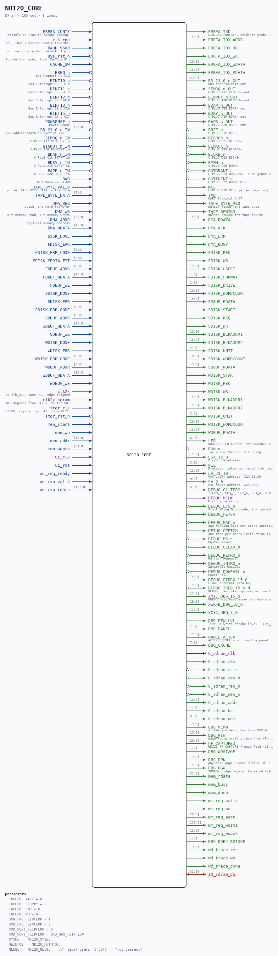
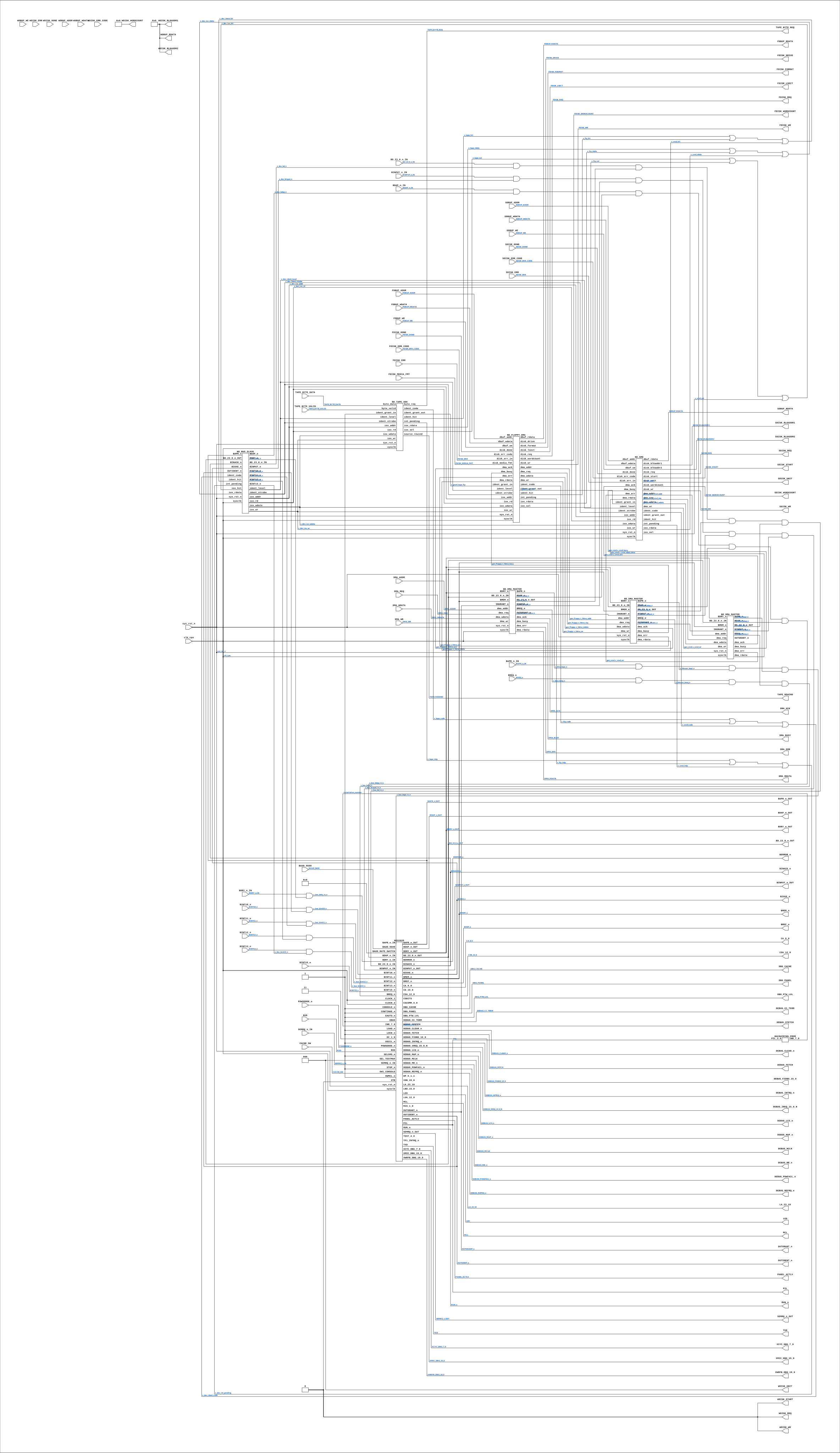
Schematic
Drawn from the Verilog: the yosys netlist of the Simulation (Verilator) build, instance CORE. Sub-modules are boxes (click the picture to open it full size; there every sub-module box links to its page, and every wire shows its Verilog name).
Description
ND120 BOARD-INDEPENDENT CORE ND3202D CPU board + the optional ND-BUS Verilog device chain. Contains NO board-specific logic: no PLL/MMCM, no power-on reset, no LED mapping, no 7-segment, no SDRAM primitive, no heartbeat counter. Every board (Basys3/sim ND120_TOP, Tang Nano 20K, future boards) instantiates this and supplies its own clock, reset and I/O. Behaviour-preserving extraction of ND120_TOP.v (14-JUL-2026): the device chain and the ND3202D instance are moved verbatim; the `ifdef ND120_VERILOG_DEVICES gate becomes the INCLUDE_* parameters. Clocking: clk_cpu is the ONE net that fed ND3202D.sysclk, CLOCK_1, CLOCK_2 and the device chain's s_dev_clk in BOTH the sim and the FPGA branch of ND120_TOP, so it collapses to a single core input. The board decides what drives it (sim: sysclk; Basys3: clk_cpu from the MMCM; Tang: clk_cpu from the rPLL). Storage seam: the core exposes the byte/disk SOURCE ports and knows nothing of SD-FAT or of the C harness. The board supplies the implementation (sim: forwarded to ND120_TOP ports, served by the C model; hardware: nd_storage / nd_storage_devices). Ronny Hansen
Parameters
| Parameter | Default |
|---|---|
INCLUDE_TAPE |
0 |
INCLUDE_FLOPPY |
0 |
INCLUDE_SMD |
0 |
INCLUDE_WD |
0 |
SMD_HAS_FLIPFLOP |
1 |
SMD_HAS_FLIPFLOP |
0 |
SMD_WCNT_FLIPFLOP |
0 |
SMD_WCNT_FLIPFLOP |
SMD_HAS_FLIPFLOP |
SYSNO |
`ND120_SYSNO |
HWINFO2 |
`ND120_HWINFO2 |
NLEGU |
`ND120_NLEGU //! legal users (8'o377 = "not present" |
Ports
| Direction | Width | Name | Description |
|---|---|---|---|
| input | 1 |
ERRFA_CONTX |
console TX line in (probe arming) |
| output | 1 |
ERRFA_TXD |
SINTRAN ERRFATAL evidence probe TX (MEM RAM probe) |
| output | [15:0] |
ERRFA_IOX_ADDR |
|
| output | 1 |
ERRFA_IOX_RD |
|
| output | 1 |
ERRFA_IOX_WR |
|
| output | [15:0] |
ERRFA_IOX_WDATA |
|
| output | [15:0] |
ERRFA_IOX_RDATA |
|
| input | 1 |
clk_cpu |
CPU + bus + device domain (ND3202D sysclk/CLOCK_1/CLOCK_2) |
| input | 1 |
BAUD_9600 |
runtime console baud select: 1 = 9600, 0 = build default (115200). Tie 1'b0 on boards without a baud switch. |
| input | 1 |
sys_rst_n (active low) |
Active-low reset, from the board's power-on reset |
| input | 1 |
CACHE_SW |
|
| input | 1 |
BREQ_n (active low) |
Bus Request C-C12 |
| input | 1 |
BINT10_n (active low) |
Bus Interrupt 10 C-A15 |
| input | 1 |
BINT11_n (active low) |
Bus Interrupt 11 C-C15 |
| input | 1 |
BINT12_n (active low) |
Bus Interrupt 12 C-A16 |
| input | 1 |
BINT13_n (active low) |
Bus Interrupt 13 C-C16 |
| input | 1 |
BINT15_n (active low) |
Bus Interrupt 15 C-C17 |
| input | 1 |
POWSENSE_n (active low) |
Power Sense |
| input | [23:0] |
BD_23_0_n_IN |
Bus address/data in (active low, pulled high) |
| output | [23:0] |
BD_23_0_n_OUT |
Bus address/data out |
| input | 1 |
SEMRQ_n_IN |
C-PLUG A17 SEMREQ~ in |
| output | 1 |
SEMRQ_n_OUT |
C-PLUG A17 SEMREQ~ out |
| input | 1 |
BINPUT_n_IN |
C-PLUG A18 BINPUT~ in |
| output | 1 |
BINPUT_n_OUT |
C-PLUG A18 BINPUT~ out |
| input | 1 |
BDAP_n_IN |
C-PLUG C18 BDAP~ in |
| output | 1 |
BDAP_n_OUT |
C-PLUG C18 BDAP~ out |
| input | 1 |
BDRY_n_IN |
C-PLUG A19 BDRY~ in |
| output | 1 |
BDRY_n_OUT |
C-PLUG A19 BDRY~ out |
| input | 1 |
BAPR_n_IN |
C-PLUG A20 BAPR~ in |
| output | 1 |
BAPR_n_OUT |
C-PLUG A20 BAPR~ out |
| output | 1 |
BREF_n (active low) |
C-PLUG B12 BREF~ |
| output | 1 |
BERROR_n (active low) |
C-PLUG B21 BERROR~ |
| output | 1 |
BINACK_n (active low) |
C-PLUG B19 BINACK~ |
| output | 1 |
BIOXE_n (active low) |
C-PLUG C19 BIOXE~ |
| output | 1 |
BMEM_n (active low) |
C-PLUG C28 BMEM~ |
| output | 1 |
OUTGRANT_n (active low) |
C-PLUG C23 OUTGRANT~ (DMA grant chain head) |
| output | 1 |
OUTIDENT_n (active low) |
C-PLUG C22 OUTIDENT~ |
| output | 1 |
MCL |
C-PLUG B20 MCL~ (after negation) |
| input | 1 |
RXD |
UART Receive A-C8 |
| output | 1 |
TXD |
UART Transmit A-C7 |
| output | 1 |
TAPE_BYTE_REQ |
pulse: fetch next tape byte |
| input | 1 |
TAPE_BYTE_VALID |
pulse: TAPE_BYTE_DATA is the byte |
| input | [7:0] |
TAPE_BYTE_DATA |
|
| output | 1 |
TAPE_REWIND |
pulse: rewind the tape source |
| input | 1 |
DMA_REQ |
pulse: one word transfer |
| input | 1 |
DMA_WR |
0 = memory read, 1 = memory write |
| input | [23:0] |
DMA_ADDR |
physical memory address |
| input | [15:0] |
DMA_WDATA |
|
| output | [15:0] |
DMA_RDATA |
|
| output | 1 |
DMA_ACK |
|
| output | 1 |
DMA_ERR |
|
| output | 1 |
DMA_BUSY |
|
| output | 1 |
FDISK_REQ |
|
| output | 1 |
FDISK_WR |
|
| output | [15:0] |
FDISK_LSECT |
|
| output | [1:0] |
FDISK_FORMAT |
|
| output | [1:0] |
FDISK_DRIVE |
|
| output | [10:0] |
FDISK_WORDCOUNT |
|
| input | 1 |
FDISK_DONE |
|
| input | 1 |
FDISK_ERR |
|
| input | [3:0] |
FDISK_ERR_CODE |
|
| input | [3:0] |
FDISK_MEDIA_FMT |
|
| input | [9:0] |
FDBUF_ADDR |
|
| input | [15:0] |
FDBUF_WDATA |
|
| input | 1 |
FDBUF_WE |
|
| output | [15:0] |
FDBUF_RDATA |
|
| output | 1 |
SDISK_START |
|
| output | 1 |
SDISK_REQ |
|
| output | 1 |
SDISK_WR |
|
| output | [15:0] |
SDISK_BLKADDR1 |
|
| output | [15:0] |
SDISK_BLKADDR2 |
|
| output | [2:0] |
SDISK_UNIT |
|
| output | [10:0] |
SDISK_WORDCOUNT |
|
| input | 1 |
SDISK_DONE |
|
| input | 1 |
SDISK_ERR |
|
| input | [3:0] |
SDISK_ERR_CODE |
|
| input | [9:0] |
SDBUF_ADDR |
|
| input | [15:0] |
SDBUF_WDATA |
|
| input | 1 |
SDBUF_WE |
|
| output | [15:0] |
SDBUF_RDATA |
|
| output | 1 |
WDISK_START |
|
| output | 1 |
WDISK_REQ |
|
| output | 1 |
WDISK_WR |
|
| output | [15:0] |
WDISK_BLKADDR1 |
|
| output | [15:0] |
WDISK_BLKADDR2 |
|
| output | [2:0] |
WDISK_UNIT |
|
| output | [10:0] |
WDISK_WORDCOUNT |
|
| input | 1 |
WDISK_DONE |
|
| input | 1 |
WDISK_ERR |
|
| input | [3:0] |
WDISK_ERR_CODE |
|
| input | [9:0] |
WDBUF_ADDR |
|
| input | [15:0] |
WDBUF_WDATA |
|
| input | 1 |
WDBUF_WE |
|
| output | [15:0] |
WDBUF_RDATA |
|
| output | [6:0] |
LED |
ND3202D LED bundle (see ND3202D.v port comment) |
| output | 1 |
RUN_n (active low) |
low while the CPU is running |
| output | [12:0] |
CSA_12_0 |
Microcode address |
| output | [3:0] |
PIL |
Processor interrupt level (for debug capture) |
| output | [13:0] |
LA_23_10 |
MAC upper address (XLA 23:10) |
| output | [9:0] |
CA_9_0 |
MAC lower address (XCA 9:0) |
| output | [4:0] |
DEBUG_CC_TERM |
{TERM_n, CC3_n, CC2_n, CC1_n, CC0_n} |
| output | 1 |
DEBUG_MCLK |
Microcycle clock |
| output | 1 |
DEBUG_LCS_n (active low) |
0 = loading microcode, 1 = loaded |
| output | 1 |
DEBUG_FETCH |
|
| output | 1 |
DEBUG_MAP_n (active low) |
one falling edge per macro instruction (see ND3202D) |
| output | 1 |
DEBUG_CFETCH |
one rise per macro instruction (CGA CFETCH) - the MIPS event |
| output | 1 |
DEBUG_MR_n (active low) |
Master Reset |
| output | 1 |
DEBUG_CLEAR_n (active low) |
|
| output | 1 |
DEBUG_REFRQ_n (active low) |
Refresh Request |
| output | 1 |
DEBUG_INTRQ_n (active low) |
Interrupt Request |
| output | 1 |
DEBUG_POWFAIL_n (active low) |
Power Fail |
| output | [15:0] |
DEBUG_FIDBO_15_0 |
FIDBO internal data bus |
| output | [15:0] |
DEBUG_IREQ_15_0_N (active low) |
DEBUG: raw interrupt-request vector (active low) |
| output | [15:0] |
XMIC_DBG_15_0 |
DEBUG: microsequencer address-advance probe (Tang 06000-hang) |
| output | [19:0] |
XWRFB_DBG_19_0 |
|
| output | [11:0] |
XCYC_DBG_7_0 |
|
| output | 1 |
DBG_PTW_LVL |
live PT write-strobe level (~EPT_n & ~WMAP_n, 27-AUG overlap probe) - unconditional: every backend has PT chips |
| output | [7:0] |
DBG_PANEL |
|
| output | [15:0] |
PANEL_ACTLV |
ACTIVE LEVEL word from the panel processor |
| output | [7:0] |
DBG_CACHE |
|
| input | 1 |
clk2x |
2x clk_cpu, same PLL, edge-aligned |
| input | 1 |
clk2x_sdram |
180 degrees from clk2x, to the SDRAM chip |
| output | 1 |
O_sdram_clk |
|
| output | 1 |
O_sdram_cke |
|
| output | 1 |
O_sdram_cs_n (active low) |
|
| output | 1 |
O_sdram_cas_n (active low) |
|
| output | 1 |
O_sdram_ras_n (active low) |
|
| output | 1 |
O_sdram_wen_n (active low) |
|
| inout | [31:0] |
IO_sdram_dq |
|
| output | [10:0] |
O_sdram_addr |
|
| output | [1:0] |
O_sdram_ba |
|
| output | [3:0] |
O_sdram_dqm |
|
| output | [15:0] |
DBG_MEMW |
write-path debug bus from MEM_43 |
| output | [15:0] |
DBG_PTW |
page-table write stream from CPU_MMU_24 (23-AUG, zero-read campaign) |
| output | [20:0] |
PF_CAPTURED |
ND120_PF_CAPTURE freeze flag (23-AUG) |
| output | [1:0] |
DBG_WDSTAGE |
|
| output | [13:0] |
DBG_PPN |
physical page number PPN[23:10] (24-AUG) |
| output | [15:0] |
DBG_PGW |
SDRAM-bridge page-write watch (24-AUG) |
| input | 1 |
stor_clk |
27 MHz crystal (pin 4) (from ND120_TANG20K_TOP.sys_clk) |
| input | 1 |
stor_rst_n (active low) |
|
| input | 1 |
mem_start |
|
| input | 1 |
mem_we |
|
| input | [19:0] |
mem_addr |
|
| input | [31:0] |
mem_wdata |
|
| output | [31:0] |
mem_rdata |
|
| output | 1 |
mem_busy |
|
| output | 1 |
mem_done |
|
| input | 1 |
ui_clk |
|
| input | 1 |
ui_rst |
|
| output | 1 |
mm_req_valid |
|
| output | 1 |
mm_req_we |
|
| output | [26:0] |
mm_req_addr |
|
| output | [127:0] |
mm_req_wdata |
|
| output | [15:0] |
mm_req_wmask |
|
| input | 1 |
mm_req_ready |
|
| input | 1 |
mm_rsp_valid |
|
| input | [127:0] |
mm_rsp_rdata |
|
| output | [7:0] |
DBG_DDR2_BRIDGE |
|
| output | [19:0] |
wd_trace_rec |
|
| output | 1 |
wd_trace_we |
|
| output | 1 |
wd_trace_done |
Verilog source
Verilog/ND120_CORE.v on GitHub.
Show the Verilog of ND120_CORE (1303 lines)
/**************************************************************************
** ND120 BOARD-INDEPENDENT CORE **
** **
** ND3202D CPU board + the optional ND-BUS Verilog device chain. **
** Contains NO board-specific logic: no PLL/MMCM, no power-on reset, no **
** LED mapping, no 7-segment, no SDRAM primitive, no heartbeat counter. **
** Every board (Basys3/sim ND120_TOP, Tang Nano 20K, future boards) **
** instantiates this and supplies its own clock, reset and I/O. **
** **
** Behaviour-preserving extraction of ND120_TOP.v (14-JUL-2026): **
** the device chain and the ND3202D instance are moved verbatim; the **
** `ifdef ND120_VERILOG_DEVICES gate becomes the INCLUDE_* parameters. **
** **
** Clocking: clk_cpu is the ONE net that fed ND3202D.sysclk, CLOCK_1, **
** CLOCK_2 and the device chain's s_dev_clk in BOTH the sim and the FPGA **
** branch of ND120_TOP, so it collapses to a single core input. The **
** board decides what drives it (sim: sysclk; Basys3: clk_cpu from the **
** MMCM; Tang: clk_cpu from the rPLL). **
** **
** Storage seam: the core exposes the byte/disk SOURCE ports and knows **
** nothing of SD-FAT or of the C harness. The board supplies the **
** implementation (sim: forwarded to ND120_TOP ports, served by the C **
** model; hardware: nd_storage / nd_storage_devices). **
** **
** Ronny Hansen **
***************************************************************************/
//! @title ND120 board-independent core (ND3202D + ND-BUS device chain)
//! @author Ronny Hansen
// Back-wiring PROM defaults (ND120_SYSNO / ND120_HWINFO2 / ND120_NLEGU and the
// "not present" sentinels). Included here as well as in BACKWIRING_PROM.v so
// the macros are defined no matter which of the two files the toolchain reads
// first - the file is `ifndef-guarded, so including it twice is harmless.
`include "nd120_backwiring_defaults.vh"
module ND120_CORE #(
// Device chain population. Each device is instantiated in a generate
// block; when absent its shared-net contributions are tied inactive so
// the OR-buses, the IDENT chain, the DMA grant chain and the bus
// wired-AND all stay valid expressions (graceful degradation).
parameter INCLUDE_TAPE = 0, //! ND_TAPE_400 papertape at 400
parameter INCLUDE_FLOPPY = 0, //! ND_FLOPPY_DMA floppy 1560 (DMA flavor)
parameter INCLUDE_SMD = 0, //! ND_SMD disk at 1540
parameter INCLUDE_WD = 0, //! ND_WINCHESTER disk at 500 (ST506/8 inch)
// SMD controller type (passed straight to ND_SMD's HAS_WC_FLIPFLOP strap;
// see docs/design/SMD-CONTROLLER-TYPE-SEAM.md). 0 = ECC / BIG-DISC card
// (core-address / word-count registers load in a SINGLE write) - THE DEFAULT,
// because this is the card that BOOTS: the mass-storage microcode writes the
// word counter ONCE with 002000, which loads 1024 words only on a single-
// write card. On a flip-flop card that single write lands in the HI byte and
// the count stays 0, so the boot would transfer nothing. 1 = 15/10 MHz card
// (24-bit registers loaded HI-then-LO by TWO writes).
//
// Default is define-driven so a plain build boots with NO file edit, exactly
// like BOARD_CLK_FREQ / ND120_SYSNO. The 15 MHz two-write card is the opt-in:
// build with EXTRA_VDEFINES="-DND120_SMD_15MHZ" (or set the parameter from a
// higher instance) to select it. Absent the define it stays 0 = the ECC
// single-write card that boots the image.
`ifdef ND120_SMD_15MHZ
parameter SMD_HAS_FLIPFLOP = 1,
`else
parameter SMD_HAS_FLIPFLOP = 0,
`endif
// WORD-COUNTER protocol. Follows the card type. A card with a
// single-access word counter is NOT a documented controller - I built one
// briefly to reconcile DISC-TEMA with the mass-load microcode, before the
// PROM listing showed the microcode is simply written for a single-access
// card. Override only for experiments, never as a shipping configuration.
`ifdef ND120_SMD_WCNT_SINGLE
parameter SMD_WCNT_FLIPFLOP = 0,
`else
parameter SMD_WCNT_FLIPFLOP = SMD_HAS_FLIPFLOP,
`endif
// Back-wiring PROM (installation number) contents. These are what SINTRAN's
// GCPUNR reads with VERSN through IDBS,INR=35, and they are meant to be
// fixed into a bitstream at synthesis time. Defaults (and the -D override
// macros ND120_SYSNO / ND120_HWINFO2 / ND120_NLEGU) live in
// Shared/support/nd120_backwiring_defaults.vh; the PROM model and the full
// signal-path citations are in Shared/support/BACKWIRING_PROM.v; the whole
// mechanism is written up in docs/backwiring-prom-installation-number.md.
parameter [15:0] SYSNO = `ND120_SYSNO, //! CPU NUMBER (16'hFFFF = "not present")
parameter [15:0] HWINFO2 = `ND120_HWINFO2, //! CPU TYPE (16'hFFFF = "not present")
parameter [ 7:0] NLEGU = `ND120_NLEGU //! legal users (8'o377 = "not present")
) (
`ifdef ND120_ERRFA_PROBE
input wire ERRFA_CONTX, // console TX line in (probe arming)
output wire ERRFA_TXD, // SINTRAN ERRFATAL evidence probe TX (MEM RAM probe)
// device-chain IOX seam, exported for the board-level WD-IOX ring
output wire [15:0] ERRFA_IOX_ADDR,
output wire ERRFA_IOX_RD,
output wire ERRFA_IOX_WR,
output wire [15:0] ERRFA_IOX_WDATA,
output wire [15:0] ERRFA_IOX_RDATA,
`endif
/***************************************************
* (a) CLOCK / RESET *
***************************************************/
input wire clk_cpu, //! CPU + bus + device domain (ND3202D sysclk/CLOCK_1/CLOCK_2)
input wire BAUD_9600, //! runtime console baud select: 1 = 9600, 0 = build default (115200). Tie 1'b0 on boards without a baud switch.
input wire sys_rst_n, //! Active-low reset, from the board's power-on reset
/***************************************************
* (b) CONSOLE SWITCHES *
***************************************************/
//! The ND-100 console's SW1, the cache on/off switch (sheet 25 CON):
//! 1 = cache on, 0 = every access goes to main memory and the CSR
//! reports the cache disabled. Until 29-AUG-2026 this was tied high
//! inside the core; now the board decides. Nexys 4 DDR: slide switch
//! sw[4]. Tang / Verilator: tied high (the Tang builds with
//! ND120_NO_CACHE anyway, which overrides this to off).
//! Already synchronised by the board top; treat it as slow-changing
//! but not glitch-free - the real switch was a toggle on the console.
input wire CACHE_SW,
/***************************************************
* (e) ND-100 C-PLUG BUS *
* Always present on the core; the board either *
* drives it (sim harness) or ties it off (FPGA). *
***************************************************/
input wire BREQ_n, //! Bus Request C-C12
input wire BINT10_n, //! Bus Interrupt 10 C-A15
input wire BINT11_n, //! Bus Interrupt 11 C-C15
input wire BINT12_n, //! Bus Interrupt 12 C-A16
input wire BINT13_n, //! Bus Interrupt 13 C-C16
input wire BINT15_n, //! Bus Interrupt 15 C-C17
input wire POWSENSE_n, //! Power Sense
input wire [23:0] BD_23_0_n_IN, //! Bus address/data in (active low, pulled high)
output wire [23:0] BD_23_0_n_OUT, //! Bus address/data out
input wire SEMRQ_n_IN, //! C-PLUG A17 SEMREQ~ in
output wire SEMRQ_n_OUT, //! C-PLUG A17 SEMREQ~ out
input wire BINPUT_n_IN, //! C-PLUG A18 BINPUT~ in
output wire BINPUT_n_OUT, //! C-PLUG A18 BINPUT~ out
input wire BDAP_n_IN, //! C-PLUG C18 BDAP~ in
output wire BDAP_n_OUT, //! C-PLUG C18 BDAP~ out
input wire BDRY_n_IN, //! C-PLUG A19 BDRY~ in
output wire BDRY_n_OUT, //! C-PLUG A19 BDRY~ out
input wire BAPR_n_IN, //! C-PLUG A20 BAPR~ in
output wire BAPR_n_OUT, //! C-PLUG A20 BAPR~ out
output wire BREF_n, //! C-PLUG B12 BREF~
output wire BERROR_n, //! C-PLUG B21 BERROR~
output wire BINACK_n, //! C-PLUG B19 BINACK~
output wire BIOXE_n, //! C-PLUG C19 BIOXE~
output wire BMEM_n, //! C-PLUG C28 BMEM~
output wire OUTGRANT_n, //! C-PLUG C23 OUTGRANT~ (DMA grant chain head)
output wire OUTIDENT_n, //! C-PLUG C22 OUTIDENT~
output wire MCL, //! C-PLUG B20 MCL~ (after negation)
/***************************************************
* (d) UART (A-PLUG console) *
***************************************************/
input wire RXD, //! UART Receive A-C8
output wire TXD, //! UART Transmit A-C7
/***************************************************
* (c) STORAGE BACKEND SOURCE PORTS *
* Meaningful only for the devices the INCLUDE_* *
* parameters populate; the rest read as tied-off *
* outputs and ignored inputs. (Verilog cannot *
* make a port list depend on a parameter, so the *
* ports are declared unconditionally and the *
* generate-else drives the outputs inactive.) *
***************************************************/
// Papertape byte source (INCLUDE_TAPE)
output wire TAPE_BYTE_REQ, //! pulse: fetch next tape byte
input wire TAPE_BYTE_VALID, //! pulse: TAPE_BYTE_DATA is the byte
input wire [7:0] TAPE_BYTE_DATA,
output wire TAPE_REWIND, //! pulse: rewind the tape source
// DMA test client (INCLUDE_FLOPPY || INCLUDE_SMD: it is the grant-chain head)
input wire DMA_REQ, //! pulse: one word transfer
input wire DMA_WR, //! 0 = memory read, 1 = memory write
input wire [23:0] DMA_ADDR, //! physical memory address
input wire [15:0] DMA_WDATA,
output wire [15:0] DMA_RDATA,
output wire DMA_ACK,
output wire DMA_ERR,
output wire DMA_BUSY,
// Floppy disk-image backend (INCLUDE_FLOPPY)
output wire FDISK_REQ,
output wire FDISK_WR,
output wire [15:0] FDISK_LSECT,
output wire [1:0] FDISK_FORMAT,
output wire [1:0] FDISK_DRIVE,
output wire [10:0] FDISK_WORDCOUNT,
input wire FDISK_DONE,
input wire FDISK_ERR,
input wire [ 3:0] FDISK_ERR_CODE,
//! media format from the image size (deviceFloppyDMA.c READ FORMAT):
//! {doubleDensity, doubleSided, bytesPerSector[1:0]}
input wire [3:0] FDISK_MEDIA_FMT,
input wire [9:0] FDBUF_ADDR,
input wire [15:0] FDBUF_WDATA,
input wire FDBUF_WE,
output wire [15:0] FDBUF_RDATA,
// SMD disk backend (INCLUDE_SMD)
output wire SDISK_START,
output wire SDISK_REQ,
output wire SDISK_WR,
output wire [15:0] SDISK_BLKADDR1,
output wire [15:0] SDISK_BLKADDR2,
output wire [2:0] SDISK_UNIT,
output wire [10:0] SDISK_WORDCOUNT,
input wire SDISK_DONE,
input wire SDISK_ERR,
input wire [ 3:0] SDISK_ERR_CODE,
input wire [9:0] SDBUF_ADDR,
input wire [15:0] SDBUF_WDATA,
input wire SDBUF_WE,
output wire [15:0] SDBUF_RDATA,
// Winchester disk backend (INCLUDE_WD). Same port shape as the SMD one:
// the card reuses nd_storage_disc_adapter with Winchester geometry, since
// that adapter has nothing SMD-specific in it (see the adapter header and
// ND-BUS-DEVICES/WINCHESTER/sim/nd_winchester_adapter_tb.v).
output wire WDISK_START,
output wire WDISK_REQ,
output wire WDISK_WR,
output wire [15:0] WDISK_BLKADDR1,
output wire [15:0] WDISK_BLKADDR2,
output wire [2:0] WDISK_UNIT,
output wire [10:0] WDISK_WORDCOUNT,
input wire WDISK_DONE,
input wire WDISK_ERR,
input wire [ 3:0] WDISK_ERR_CODE,
input wire [9:0] WDBUF_ADDR,
input wire [15:0] WDBUF_WDATA,
input wire WDBUF_WE,
output wire [15:0] WDBUF_RDATA,
/***************************************************
* (f) DEBUG / STATUS (all outputs) *
***************************************************/
output wire [6:0] LED, //! ND3202D LED bundle (see ND3202D.v port comment)
output wire RUN_n, //! low while the CPU is running
output wire [12:0] CSA_12_0, //! Microcode address
output wire [ 3:0] PIL, //! Processor interrupt level (for debug capture)
output wire [13:0] LA_23_10, //! MAC upper address (XLA 23:10)
output wire [9:0] CA_9_0, //! MAC lower address (XCA 9:0)
output wire [4:0] DEBUG_CC_TERM, //! {TERM_n, CC3_n, CC2_n, CC1_n, CC0_n}
output wire DEBUG_MCLK, //! Microcycle clock
output wire DEBUG_LCS_n, //! 0 = loading microcode, 1 = loaded
output wire DEBUG_FETCH,
output wire DEBUG_MAP_n, //! one falling edge per macro instruction (see ND3202D)
output wire DEBUG_CFETCH, //! one rise per macro instruction (CGA CFETCH) - the MIPS event
output wire DEBUG_MR_n, //! Master Reset
output wire DEBUG_CLEAR_n,
output wire DEBUG_REFRQ_n, //! Refresh Request
output wire DEBUG_INTRQ_n, //! Interrupt Request
output wire DEBUG_POWFAIL_n, //! Power Fail
output wire [15:0] DEBUG_FIDBO_15_0, //! FIDBO internal data bus
output wire [15:0] DEBUG_IREQ_15_0_N, //! DEBUG: raw interrupt-request vector (active low)
output wire [15:0] XMIC_DBG_15_0, //! DEBUG: microsequencer address-advance probe (Tang 06000-hang)
//! DEBUG: register-file B port as {LBA_3_0, B_15_0}. At microcode address
//! 002156 (STERR) the microcode does "B,R2 ALUF,PASSB", so this carries the
//! self-test error number that STERR exists to display.
output wire [19:0] XWRFB_DBG_19_0,
//! DEBUG: cycle-controller terminate-plane inputs, see CYC_36.v.
//! [0] SHORT_n [1] SLOW_n [2] HIT [3] BRK_n [4] DLY0_n [5] DLY1_n [7:6] CSDELAY
output wire [11:0] XCYC_DBG_7_0,
output wire DBG_PTW_LVL, //! live PT write-strobe level (~EPT_n & ~WMAP_n, 27-AUG overlap probe) - unconditional: every backend has PT chips
//! Operator-panel status in MC68705 Port-D order - see the port comment in
//! ND3202D.v. Unconditional for the same reason DBG_PTW_LVL is: a debug
//! signal that anything outside a conditional touches must be declared
//! outside every conditional, or it vanishes on some builds and not others.
output wire [7:0] DBG_PANEL,
output wire [15:0] PANEL_ACTLV, //! ACTIVE LEVEL word from the panel processor
//! DEBUG: cache-write gating bus, straight through from ND3202D. Bit
//! layout and the reason are in CPU_MMU_24.v's DBG_CACHE port comment.
output wire [7:0] DBG_CACHE
`ifdef MAIN_RAM_SDRAM
/***************************************************
* (b) RAM BACKEND - SDRAM PHY pass-through only *
* RAM lives INSIDE ND3202D (MEM_43 -> MEM_RAM_49);*
* under MAIN_RAM_SDRAM the PHY pins are threaded *
* up through ND3202D and out to the board. *
* Absent entirely on sim/Basys3 (on-chip BRAM). *
***************************************************/
,
input wire clk2x, //! 2x clk_cpu, same PLL, edge-aligned
input wire clk2x_sdram, //! 180 degrees from clk2x, to the SDRAM chip
output wire O_sdram_clk,
output wire O_sdram_cke,
output wire O_sdram_cs_n,
output wire O_sdram_cas_n,
output wire O_sdram_ras_n,
output wire O_sdram_wen_n,
inout wire [31:0] IO_sdram_dq,
output wire [10:0] O_sdram_addr,
output wire [ 1:0] O_sdram_ba,
output wire [ 3:0] O_sdram_dqm,
output wire [15:0] DBG_MEMW, //! write-path debug bus from MEM_43
output wire [15:0] DBG_PTW, //! page-table write stream from CPU_MMU_24 (23-AUG, zero-read campaign)
output wire [20:0] PF_CAPTURED, //! ND120_PF_CAPTURE freeze flag (23-AUG)
//! DEBUG stage timer (24-AUG-2026): [0] Winchester controller active,
//! [1] the Winchester's DMA master busy. Used to find where a disc
//! operation's ~1 s of wall clock actually goes.
output wire [1:0] DBG_WDSTAGE,
output wire [13:0] DBG_PPN, //! physical page number PPN[23:10] (24-AUG)
output wire [15:0] DBG_PGW //! SDRAM-bridge page-write watch (24-AUG)
`ifdef ND_STORAGE_PORT
/***************************************************
* (c) STORAGE seam into the SDRAM device port *
* The board's storage stack (nd_storage_devices)*
* reaches MEM_RAM_49_SDRAM's upper-half region *
* through here. The backend forces the leading *
* address 1, so device traffic physically cannot *
* touch the CPU's half of the chip. *
* stor_clk is an INDEPENDENT domain (the SD stack *
* needs 27 MHz for a spec-legal identification *
* clock, whatever VARIANT the CPU runs at); the *
* backend toggle-CDCs it into clk2x. *
***************************************************/
,
input wire stor_clk, //! 27 MHz crystal (pin 4) (from ND120_TANG20K_TOP.sys_clk)
input wire stor_rst_n,
input wire mem_start,
input wire mem_we,
input wire [19:0] mem_addr,
input wire [31:0] mem_wdata,
output wire [31:0] mem_rdata,
output wire mem_busy,
output wire mem_done
`endif
`endif
`ifdef MAIN_RAM_DDR2
/***************************************************
* (b2) RAM BACKEND - DDR2 client pass-through *
* RAM lives INSIDE ND3202D (MEM_43 -> *
* MEM_RAM_49_DDR2); the ui_clk-domain client *
* port is threaded up to the board top, where *
* nd_ddr2_arb shares the MIG with the storage *
* region. Absent in every other build. *
***************************************************/
,
input wire ui_clk,
input wire ui_rst,
output wire mm_req_valid,
output wire mm_req_we,
output wire [ 26:0] mm_req_addr,
output wire [127:0] mm_req_wdata,
output wire [ 15:0] mm_req_wmask,
input wire mm_req_ready,
input wire mm_rsp_valid,
input wire [127:0] mm_rsp_rdata,
output wire [ 7:0] DBG_DDR2_BRIDGE
`endif
`ifdef TANG_WD_TRACE_DUMP
,
// Winchester IOX trace tap, brought out for the board-level capture and
// UART dump. Present ONLY under TANG_WD_TRACE_DUMP - the normal build
// never carries it.
output wire [19:0] wd_trace_rec,
output wire wd_trace_we,
output wire wd_trace_done
`endif
);
/**********************************************
* Constants that used to live in ND120_TOP *
***********************************************/
// Installation number (read using IDB Source = 035)
//
// Was a single hardwired 8'd123 for EVERY PIL value, which made SINTRAN's
// GCPUNR signature check (bytes 6/7 must read 0x55/0xAA) fail, so the CPU
// NUMBER / CPU TYPE / NLEGU in the PROM could never be reported. It is now a
// real 16-byte back-wiring PROM addressed by PIL[3:0] - see the instance of
// BACKWIRING_PROM further down and docs/backwiring-prom-installation-number.md.
wire [7:0] installation_number;
wire s_high = 1'b1;
wire s_low = 1'b0;
wire [1:0] oc_select = 2'b11; // 11 = clock input XTAL1 (full speed)
wire [2:0] s_SEL_TESTMUX = 3'b000; // 000 = TESTMUX = 0
// 8 = 9600 baud (ref BAUDV page 158 in microcode)
wire [3:0] s_baud_rate_switch = 4'b1000;
/**********************************************
* CPU-board debug wires kept alive *
* (Run120.cpp reads s_csbits hierarchically) *
***********************************************/
(* keep = "true", DONT_TOUCH = "true" *) wire [4:0] s_test_4_0; // Test pads
(* keep = "true", DONT_TOUCH = "true" *) wire [4:0] s_dp_5_1_n; // Datapath 5-1
(* keep = "true", DONT_TOUCH = "true" *) wire s_tp1_intrq_n; // TP1 INTRQ_n
(* keep = "true", DONT_TOUCH = "true" *) wire [63:0] s_csbits; // Microcode CPU BITS
/**********************************************
* Verilog external-bus devices (optional) *
* ND-BUS-DEVICES: bus slave + papertape 400 *
* + floppy 1560 + SMD 1540 and their DMA *
* masters. Wired-AND onto the active-low bus *
* inputs of the CPU board. *
***********************************************/
localparam ANY_DEVICE = (INCLUDE_TAPE != 0) || (INCLUDE_FLOPPY != 0) || (INCLUDE_SMD != 0) || (INCLUDE_WD != 0);
// The DMA test master is the head of the DMA grant chain (its INGRANT_n is
// the CPU's OUTGRANT_n), so it must exist whenever any bus master exists.
localparam ANY_DMA_MASTER = (INCLUDE_FLOPPY != 0) || (INCLUDE_SMD != 0) || (INCLUDE_WD != 0);
// Every device shares this one clock with the CPU board.
wire s_dev_clk = clk_cpu;
// ---- device timing expressed as TIME, converted here to clk_cpu cycles ---
// BOARD_CLK_FREQ is the actual clk_cpu frequency in Hz. The Tang defines it
// in fpga/tang-nano-20k/src/tang20k_defines.v: 6_750_000 for the default
// slow bring-up (the PLL gives CLKOUT 13.5 MHz and clk_cpu = CLKOUT/2),
// 27_000_000 full speed, 3_375_000 crawl. Builds that do not define it
// (the Verilator sim) fall back to the same 100 MHz DECODE_DGA_POW uses,
// so the macro's meaning stays identical everywhere.
`ifdef BOARD_CLK_FREQ
localparam integer DEV_CLK_HZ = `BOARD_CLK_FREQ;
`else
localparam integer DEV_CLK_HZ = 100_000_000;
`endif
// SMD: how long the controller holds ACTIVE after a GO before reporting
// completion. This is a mechanical time on a real drive - a 75 MB SMD at
// 3600 rpm averages 8.3 ms of rotational latency alone, and a seek is tens
// of milliseconds - and diagnostics rely on it: DISC-TEMA reads the status
// a few thousand clocks after activating and reports "Controller not active
// after activate" if the operation has already finished. 8 ms is close to
// the real rotational figure and leaves a wide margin over that check at
// every clock variant (54,000 cycles at 6.75 MHz, 216,000 at 27 MHz).
localparam integer SMD_DELAY_MS = 8;
// The delay is a WALL-CLOCK time, so the CYCLE count it becomes depends on
// DEV_CLK_HZ: 216,000 cycles on the Tang (27 MHz) but 800,000 in Verilator,
// which falls back to 100 MHz. The CPU executes per CYCLE, so the sim gives
// a spinning driver 3.7x MORE instructions before the card completes - and
// DISC-TEMA's wait for the seek is a software loop with a bounded count.
// ND120_DEV_DELAY_TICKS overrides the cycle count directly so a sim run can
// be made cycle-identical to silicon. Overriding is a DIAGNOSTIC lever, not
// a fix: it changes what the drive models, so leave it undefined unless a
// specific experiment needs it.
`ifdef ND120_DEV_DELAY_TICKS
localparam [31:0] SMD_DELAY_TICKS = `ND120_DEV_DELAY_TICKS;
`else
localparam [31:0] SMD_DELAY_TICKS = (DEV_CLK_HZ / 1000) * SMD_DELAY_MS;
`endif
// TESTED AND EXONERATED 05-AUG-2026, confirmed 06-AUG: the completion
// latency was never the cause of DISC-TEMA's "Memory address Register not
// as expected". The real fault was the CPU zeroing the A register at the
// end of every IOX WRITE (the CDLBD 74646's bidirectional LBD pin was
// transcribed as separate in/out nets, so the DSTB_n-rise capture read a
// dead bus and the microcode's unconditional A := DBR loaded 0). Fixed
// 06-AUG-2026 in CPU-BOARD-3202/circuit/BIF_DPATH_9.v (one OR-term restores
// the pin node); verified clean on silicon and in simulation.
`ifndef MAIN_RAM_SDRAM
// DBG_WDSTAGE is an output port only in the MAIN_RAM_SDRAM section of the
// port list, but the Winchester generate below drives it unconditionally.
// Without this fallback the non-SDRAM builds (Verilator, DDR2) create an
// IMPLICIT 1-bit net - which Verilator -Wall treats as a hard error
// (found 30-AUG-2026 when runSim stopped verilating). Same rule as the
// DBG_CACHE port comment: a debug wire touched outside a conditional must
// exist in every build.
wire [1:0] DBG_WDSTAGE;
`endif
// Bus-slave contributions onto the CPU's bus inputs (active low)
wire [23:0] s_dev_bd_n;
wire s_dev_binput_n, s_dev_bdap_n, s_dev_bdry_n;
wire s_dev_bint10_n, s_dev_bint11_n, s_dev_bint12_n, s_dev_bint13_n;
// IOX fan-out from the bus slave to the device cores
// ND120_ILA_MARK_DEBUG (Nexys build.tcl -tclargs ila): keep the device
// IOX seam nets for the JTAG ILA - which register the CPU polls during
// the LIST-FILE-NAMES runaway and what the device answers (24-AUG).
// No functional effect; the define is set only by that build flag.
`ifdef ND120_ILA_MARK_DEBUG
(* mark_debug = "true" *)
`endif
wire [15:0] s_dev_iox_addr;
wire [15:0] s_dev_iox_wdata;
`ifdef ND120_ILA_MARK_DEBUG
(* mark_debug = "true" *)
`endif
wire s_dev_iox_wr;
`ifdef ND120_ILA_MARK_DEBUG
(* mark_debug = "true" *)
`endif
wire s_dev_iox_rd;
`ifdef ND120_ILA_MARK_DEBUG
(* mark_debug = "true" *)
`endif
wire s_dev_ident_strobe;
`ifdef ND120_ILA_MARK_DEBUG
(* mark_debug = "true" *)
`endif
wire [3:0] s_dev_ident_level;
// OR-bus contributions per device core (tape, floppy, SMD)
wire [15:0] s_tape_rdata, s_flp_rdata, s_smd_rdata, s_wd_rdata;
wire [3:0] s_tape_intp, s_flp_intp, s_smd_intp, s_wd_intp;
wire s_tape_hit, s_flp_hit, s_smd_hit, s_wd_hit;
wire [15:0] s_tape_code, s_flp_code, s_smd_code, s_wd_code;
// Per-core IOX address-match. When NO core owns the captured IOX address the
// slave must answer nothing (no BDRY) so the CPU bus-times-out into the
// level-14 IOX error, instead of the slave answering every address.
wire s_tape_sel, s_flp_sel, s_smd_sel, s_wd_sel;
// IDENT daisy chain: head -> tape -> floppy -> SMD (absent stage = pass-through)
`ifdef ND120_ILA_MARK_DEBUG
(* mark_debug = "true" *)
`endif
wire s_grant_tape_flp; // ident chain: tape -> floppy
wire s_grant_flp_smd; // ident chain: floppy -> SMD
wire s_grant_smd_wd; // ident chain: SMD -> Winchester
`ifdef ND120_ILA_MARK_DEBUG
(* mark_debug = "true" *)
`endif
wire [15:0] s_dev_iox_rdata = s_tape_rdata | s_flp_rdata | s_smd_rdata | s_wd_rdata;
`ifdef ND120_ILA_MARK_DEBUG
(* mark_debug = "true" *)
`endif
wire [3:0] s_dev_int_pending = s_tape_intp | s_flp_intp | s_smd_intp | s_wd_intp;
`ifdef ND120_ILA_MARK_DEBUG
(* mark_debug = "true" *)
`endif
wire s_dev_ident_hit = s_tape_hit | s_flp_hit | s_smd_hit | s_wd_hit;
`ifdef ND120_ILA_MARK_DEBUG
(* mark_debug = "true" *)
`endif
wire [15:0] s_dev_ident_code = s_tape_code | s_flp_code | s_smd_code | s_wd_code;
wire s_dev_iox_hit = s_tape_sel | s_flp_sel | s_smd_sel | s_wd_sel;
`ifdef ND120_ERRFA_PROBE
assign ERRFA_IOX_ADDR = s_dev_iox_addr;
assign ERRFA_IOX_RD = s_dev_iox_rd;
assign ERRFA_IOX_WR = s_dev_iox_wr;
assign ERRFA_IOX_WDATA = s_dev_iox_wdata;
assign ERRFA_IOX_RDATA = s_dev_iox_rdata;
`endif
// DMA grant chain (active low): CPU OUTGRANT_n -> test master -> floppy
// master -> SMD master. Declared up front: s_grant_fdma_smdm_n is used by
// the floppy master before the SMD master is instantiated.
wire s_grant_dma_fdma_n; // grant chain: test DMA master -> floppy master
wire s_grant_fdma_smdm_n; // grant chain: floppy master -> SMD master
wire s_grant_smdm_wdm_n; // grant chain: SMD master -> Winchester master
// Per-master bus contributions (active low; tied high when the master is absent)
wire [23:0] s_dma_bd_n, s_fdmam_bd_n, s_smdm_bd_n, s_wdm_bd_n;
wire s_dma_breq_n, s_fdmam_breq_n, s_smdm_breq_n, s_wdm_breq_n;
wire s_dma_bapr_n, s_fdmam_bapr_n, s_smdm_bapr_n, s_wdm_bapr_n;
wire s_dma_binput_n, s_fdmam_binput_n, s_smdm_binput_n, s_wdm_binput_n;
wire s_dma_bdap_n, s_fdmam_bdap_n, s_smdm_bdap_n, s_wdm_bdap_n;
/*---------------------------------------------
* ND-BUS slave shell (present with any device)
*--------------------------------------------*/
generate
if (ANY_DEVICE) begin : gen_bus_slave
ND_BUS_SLAVE BUS_SLAVE (
.sysclk(s_dev_clk),
.sys_rst_n(sys_rst_n),
.BD_23_0_n_OUT(BD_23_0_n_OUT),
.BD_23_0_n_IN(s_dev_bd_n),
.BAPR_n(BAPR_n_OUT),
.BIOXE_n(BIOXE_n),
.BINACK_n(BINACK_n),
.OUTIDENT_n(OUTIDENT_n),
.BINPUT_n(s_dev_binput_n),
.BDAP_n(s_dev_bdap_n),
.BDRY_n(s_dev_bdry_n),
.BINT10_n(s_dev_bint10_n),
.BINT11_n(s_dev_bint11_n),
.BINT12_n(s_dev_bint12_n),
.BINT13_n(s_dev_bint13_n),
.iox_addr(s_dev_iox_addr),
.iox_wr(s_dev_iox_wr),
.iox_wdata(s_dev_iox_wdata),
.iox_rd(s_dev_iox_rd),
.iox_rdata(s_dev_iox_rdata),
.iox_hit(s_dev_iox_hit),
.int_pending(s_dev_int_pending),
.ident_strobe(s_dev_ident_strobe),
.ident_level(s_dev_ident_level),
.ident_hit(s_dev_ident_hit),
.ident_code(s_dev_ident_code)
);
end else begin : gen_no_bus_slave
// No devices: contribute nothing to the wired-AND, drive no IOX.
assign s_dev_bd_n = 24'hFFFFFF;
assign s_dev_binput_n = 1'b1;
assign s_dev_bdap_n = 1'b1;
assign s_dev_bdry_n = 1'b1;
assign s_dev_bint10_n = 1'b1;
assign s_dev_bint11_n = 1'b1;
assign s_dev_bint12_n = 1'b1;
assign s_dev_bint13_n = 1'b1;
assign s_dev_iox_addr = 16'd0;
assign s_dev_iox_wdata = 16'd0;
assign s_dev_iox_wr = 1'b0;
assign s_dev_iox_rd = 1'b0;
assign s_dev_ident_strobe = 1'b0;
assign s_dev_ident_level = 4'd0;
end
endgenerate
/*---------------------------------------------
* Papertape reader 400 (byte source on board)
*--------------------------------------------*/
generate
if (INCLUDE_TAPE != 0) begin : gen_tape
ND_TAPE_400 #(
.BASE_ADDR (16'o000400),
.IDENT_CODE(16'o000002),
.INT_LEVEL (4'd12)
) TAPE_400 (
.sysclk(s_dev_clk),
.sys_rst_n(sys_rst_n),
.iox_addr(s_dev_iox_addr),
.iox_wr(s_dev_iox_wr),
.iox_wdata(s_dev_iox_wdata),
.iox_rd(s_dev_iox_rd),
.iox_rdata(s_tape_rdata),
.iox_sel(s_tape_sel),
.int_pending(s_tape_intp),
.ident_strobe(s_dev_ident_strobe),
.ident_level(s_dev_ident_level),
.ident_grant_in(1'b1), // chain head
.ident_grant_out(s_grant_tape_flp),
.ident_hit(s_tape_hit),
.ident_code(s_tape_code),
.byte_req(TAPE_BYTE_REQ),
.byte_valid(TAPE_BYTE_VALID),
.byte_data(TAPE_BYTE_DATA),
.source_rewind(TAPE_REWIND)
);
end else begin : gen_no_tape
assign s_tape_rdata = 16'd0;
assign s_tape_sel = 1'b0;
assign s_tape_intp = 4'd0;
assign s_tape_hit = 1'b0;
assign s_tape_code = 16'd0;
assign s_grant_tape_flp = 1'b1; // pass the chain head through
assign TAPE_BYTE_REQ = 1'b0;
assign TAPE_REWIND = 1'b0;
end
endgenerate
/*---------------------------------------------
* Floppy 1560, DMA flavor (Ronny's choice
* 11-JUL): the controller masters the bus
* through its own ND_DMA_MASTER, second in the
* grant chain behind the DMA test master.
*--------------------------------------------*/
generate
if (INCLUDE_FLOPPY != 0) begin : gen_floppy
wire s_fdma_req, s_fdma_wr;
wire [23:0] s_fdma_addr;
wire [15:0] s_fdma_wdata, s_fdma_rdata;
wire s_fdma_ack, s_fdma_err, s_fdma_busy;
ND_FLOPPY_DMA #(
.BASE_ADDR (16'o001560),
.IDENT_CODE(16'o000021),
.INT_LEVEL (4'd11)
) FLOPPY_1560 (
.sysclk(s_dev_clk),
.sys_rst_n(sys_rst_n),
.iox_addr(s_dev_iox_addr),
.iox_wr(s_dev_iox_wr),
.iox_wdata(s_dev_iox_wdata),
.iox_rd(s_dev_iox_rd),
.iox_rdata(s_flp_rdata),
.iox_sel(s_flp_sel),
.int_pending(s_flp_intp),
.ident_strobe(s_dev_ident_strobe),
.ident_level(s_dev_ident_level),
.ident_grant_in(s_grant_tape_flp),
.ident_grant_out(s_grant_flp_smd),
.ident_hit(s_flp_hit),
.ident_code(s_flp_code),
.dma_req(s_fdma_req),
.dma_wr(s_fdma_wr),
.dma_addr(s_fdma_addr),
.dma_wdata(s_fdma_wdata),
.dma_rdata(s_fdma_rdata),
.dma_ack(s_fdma_ack),
.dma_err(s_fdma_err),
.dma_busy(s_fdma_busy),
.disk_req(FDISK_REQ),
.disk_wr(FDISK_WR),
.disk_lsect(FDISK_LSECT),
.disk_format(FDISK_FORMAT),
.disk_drive(FDISK_DRIVE),
.disk_wordcount(FDISK_WORDCOUNT),
.disk_done(FDISK_DONE),
.disk_err_in(FDISK_ERR),
.disk_err_code(FDISK_ERR_CODE),
.disk_media_fmt(FDISK_MEDIA_FMT),
.dbuf_addr(FDBUF_ADDR),
.dbuf_wdata(FDBUF_WDATA),
.dbuf_we(FDBUF_WE),
.dbuf_rdata(FDBUF_RDATA)
);
ND_DMA_MASTER #(
.TIMEOUT_TICKS(16'd8192)
) FLOPPY_DMA_MASTER (
.sysclk(s_dev_clk),
.sys_rst_n(sys_rst_n),
.dma_req(s_fdma_req),
.dma_wr(s_fdma_wr),
.dma_addr(s_fdma_addr),
.dma_wdata(s_fdma_wdata),
.dma_rdata(s_fdma_rdata),
.dma_ack(s_fdma_ack),
.dma_err(s_fdma_err),
.dma_busy(s_fdma_busy),
.BREQ_n(s_fdmam_breq_n),
.INGRANT_n(s_grant_dma_fdma_n),
.OUTGRANT_n(s_grant_fdma_smdm_n),
.BMEM_n(BMEM_n),
.BD_23_0_n_OUT(s_fdmam_bd_n),
.BD_23_0_n_IN(BD_23_0_n_OUT),
.BAPR_n(s_fdmam_bapr_n),
.BINPUT_n(s_fdmam_binput_n),
.BDAP_n(s_fdmam_bdap_n),
.BDRY_n(BDRY_n_OUT)
);
end else begin : gen_no_floppy
assign s_flp_rdata = 16'd0;
assign s_flp_sel = 1'b0;
assign s_flp_intp = 4'd0;
assign s_flp_hit = 1'b0;
assign s_flp_code = 16'd0;
assign s_grant_flp_smd = s_grant_tape_flp; // ident chain pass-through
assign s_grant_fdma_smdm_n = s_grant_dma_fdma_n; // DMA grant pass-through
assign s_fdmam_bd_n = 24'hFFFFFF;
assign s_fdmam_breq_n = 1'b1;
assign s_fdmam_bapr_n = 1'b1;
assign s_fdmam_binput_n = 1'b1;
assign s_fdmam_bdap_n = 1'b1;
assign FDISK_REQ = 1'b0;
assign FDISK_WR = 1'b0;
assign FDISK_LSECT = 16'd0;
assign FDISK_FORMAT = 2'd0;
assign FDISK_DRIVE = 2'd0;
assign FDISK_WORDCOUNT = 11'd0;
assign FDBUF_RDATA = 16'd0;
end
endgenerate
/*---------------------------------------------
* SMD disk controller at 1540 with its own bus
* master, third in the grant chain
* (test master -> floppy master -> SMD master)
*--------------------------------------------*/
generate
if (INCLUDE_SMD != 0) begin : gen_smd
wire s_smd_req, s_smd_wr;
wire [23:0] s_smd_addr;
wire [15:0] s_smd_wdata, s_smd_rdata_dma;
wire s_smd_ack, s_smd_err, s_smd_busy;
ND_SMD #(
.BASE_ADDR (16'o001540),
.IDENT_CODE (16'o000017),
.INT_LEVEL (4'd11),
.DELAY_TICKS(SMD_DELAY_TICKS),
// Controller-type strap: default ECC single-write (boots the SMD
// image). Override the top-level SMD_HAS_FLIPFLOP to 1 (or build with
// -DND120_SMD_15MHZ) for the 15 MHz two-write card.
.HAS_WC_FLIPFLOP(SMD_HAS_FLIPFLOP),
.HAS_WCNT_FLIPFLOP(SMD_WCNT_FLIPFLOP)
) SMD_1540 (
.sysclk(s_dev_clk),
.sys_rst_n(sys_rst_n),
.iox_addr(s_dev_iox_addr),
.iox_wr(s_dev_iox_wr),
.iox_wdata(s_dev_iox_wdata),
.iox_rd(s_dev_iox_rd),
.iox_rdata(s_smd_rdata),
.iox_sel(s_smd_sel),
.int_pending(s_smd_intp),
.ident_strobe(s_dev_ident_strobe),
.ident_level(s_dev_ident_level),
.ident_grant_in(s_grant_flp_smd),
.ident_grant_out(s_grant_smd_wd),
.ident_hit(s_smd_hit),
.ident_code(s_smd_code),
.dma_req(s_smd_req),
.dma_wr(s_smd_wr),
.dma_addr(s_smd_addr),
.dma_wdata(s_smd_wdata),
.dma_rdata(s_smd_rdata_dma),
.dma_ack(s_smd_ack),
.dma_err(s_smd_err),
.dma_busy(s_smd_busy),
.disk_start(SDISK_START),
.disk_req(SDISK_REQ),
.disk_wr(SDISK_WR),
.disk_blkaddr1(SDISK_BLKADDR1),
.disk_blkaddr2(SDISK_BLKADDR2),
.disk_unit(SDISK_UNIT),
.disk_wordcount(SDISK_WORDCOUNT),
.disk_done(SDISK_DONE),
.disk_err_in(SDISK_ERR),
.disk_err_code(SDISK_ERR_CODE),
.dbuf_addr(SDBUF_ADDR),
.dbuf_wdata(SDBUF_WDATA),
.dbuf_we(SDBUF_WE),
.dbuf_rdata(SDBUF_RDATA)
);
ND_DMA_MASTER #(
.TIMEOUT_TICKS(16'd8192)
) SMD_DMA_MASTER (
.sysclk(s_dev_clk),
.sys_rst_n(sys_rst_n),
.dma_req(s_smd_req),
.dma_wr(s_smd_wr),
.dma_addr(s_smd_addr),
.dma_wdata(s_smd_wdata),
.dma_rdata(s_smd_rdata_dma),
.dma_ack(s_smd_ack),
.dma_err(s_smd_err),
.dma_busy(s_smd_busy),
.BREQ_n(s_smdm_breq_n),
.INGRANT_n(s_grant_fdma_smdm_n),
.OUTGRANT_n(s_grant_smdm_wdm_n),
.BMEM_n(BMEM_n),
.BD_23_0_n_OUT(s_smdm_bd_n),
.BD_23_0_n_IN(BD_23_0_n_OUT),
.BAPR_n(s_smdm_bapr_n),
.BINPUT_n(s_smdm_binput_n),
.BDAP_n(s_smdm_bdap_n),
.BDRY_n(BDRY_n_OUT)
);
end else begin : gen_no_smd
assign s_grant_smd_wd = s_grant_flp_smd; // ident chain pass-through
assign s_grant_smdm_wdm_n = s_grant_fdma_smdm_n; // DMA grant pass-through
assign s_smd_rdata = 16'd0;
assign s_smd_sel = 1'b0;
assign s_smd_intp = 4'd0;
assign s_smd_hit = 1'b0;
assign s_smd_code = 16'd0;
assign s_smdm_bd_n = 24'hFFFFFF;
assign s_smdm_breq_n = 1'b1;
assign s_smdm_bapr_n = 1'b1;
assign s_smdm_binput_n = 1'b1;
assign s_smdm_bdap_n = 1'b1;
assign SDISK_START = 1'b0;
assign SDISK_REQ = 1'b0;
assign SDISK_WR = 1'b0;
assign SDISK_BLKADDR1 = 16'd0;
assign SDISK_BLKADDR2 = 16'd0;
assign SDISK_UNIT = 3'd0;
assign SDISK_WORDCOUNT = 11'd0;
assign SDBUF_RDATA = 16'd0;
end
endgenerate
/*---------------------------------------------
* Winchester disc controller at 500 (ST506
* card 3041 / 8 inch card 3038) with its own
* bus master, fourth in the grant chain
* (test -> floppy -> SMD -> Winchester).
*
* NOTE 500-507 is the SAME IOX block as the
* CDC cartridge disc: a machine has one card
* or the other, never both.
*--------------------------------------------*/
generate
if (INCLUDE_WD != 0) begin : gen_wd
wire s_wd_req, s_wd_wr;
wire [23:0] s_wd_addr;
wire [15:0] s_wd_wdata, s_wd_rdata_dma;
wire s_wd_ack, s_wd_err, s_wd_busy;
wire s_wd_dbg_active;
ND_WINCHESTER #(
.BASE_ADDR (16'o000500),
.IDENT_CODE (16'o000001),
.INT_LEVEL (4'd11),
.DELAY_TICKS(SMD_DELAY_TICKS),
// Micropolis 1325 (the DISC-74-1) - the drive SINTRAN boots from,
// and the default in both C models. MUST match the GEO_* the
// storage adapter in front of the backend is given.
.GEO_HEADS (16'd8),
.GEO_SPT (16'd9),
.GEO_MAX_CYL(16'd1024)
) WD_500 (
.sysclk(s_dev_clk),
.sys_rst_n(sys_rst_n),
.iox_addr(s_dev_iox_addr),
.iox_wr(s_dev_iox_wr),
.iox_wdata(s_dev_iox_wdata),
.iox_rd(s_dev_iox_rd),
.iox_rdata(s_wd_rdata),
.iox_sel(s_wd_sel),
`ifdef TANG_WD_TRACE_DUMP
.trace_rec(wd_trace_rec),
.trace_we(wd_trace_we),
.trace_done(wd_trace_done),
`else
.trace_rec(),
.trace_we(),
.trace_done(),
`endif
.int_pending(s_wd_intp),
.ident_strobe(s_dev_ident_strobe),
.ident_level(s_dev_ident_level),
.ident_grant_in(s_grant_smd_wd),
.ident_grant_out(),
.ident_hit(s_wd_hit),
.ident_code(s_wd_code),
.dma_req(s_wd_req),
.dma_wr(s_wd_wr),
.dma_addr(s_wd_addr),
.dma_wdata(s_wd_wdata),
.dma_rdata(s_wd_rdata_dma),
.dma_ack(s_wd_ack),
.dma_err(s_wd_err),
.dma_busy(s_wd_busy),
.dbg_active(s_wd_dbg_active),
.disk_start(WDISK_START),
.disk_req(WDISK_REQ),
.disk_wr(WDISK_WR),
.disk_blkaddr1(WDISK_BLKADDR1),
.disk_blkaddr2(WDISK_BLKADDR2),
.disk_unit(WDISK_UNIT),
.disk_wordcount(WDISK_WORDCOUNT),
.disk_done(WDISK_DONE),
.disk_err_in(WDISK_ERR),
.disk_err_code(WDISK_ERR_CODE),
.dbuf_addr(WDBUF_ADDR),
.dbuf_wdata(WDBUF_WDATA),
.dbuf_we(WDBUF_WE),
.dbuf_rdata(WDBUF_RDATA)
);
// stage timer: [0] controller active, [1] its DMA master busy
assign DBG_WDSTAGE = {s_wd_busy, s_wd_dbg_active};
ND_DMA_MASTER #(
.TIMEOUT_TICKS(16'd8192)
) WD_DMA_MASTER (
.sysclk(s_dev_clk),
.sys_rst_n(sys_rst_n),
.dma_req(s_wd_req),
.dma_wr(s_wd_wr),
.dma_addr(s_wd_addr),
.dma_wdata(s_wd_wdata),
.dma_rdata(s_wd_rdata_dma),
.dma_ack(s_wd_ack),
.dma_err(s_wd_err),
.dma_busy(s_wd_busy),
.BREQ_n(s_wdm_breq_n),
.INGRANT_n(s_grant_smdm_wdm_n),
.OUTGRANT_n(),
.BMEM_n(BMEM_n),
.BD_23_0_n_OUT(s_wdm_bd_n),
.BD_23_0_n_IN(BD_23_0_n_OUT),
.BAPR_n(s_wdm_bapr_n),
.BINPUT_n(s_wdm_binput_n),
.BDAP_n(s_wdm_bdap_n),
.BDRY_n(BDRY_n_OUT)
);
`ifdef ND120_DMA_STALL_DBG
// ------------------------------------------------------------------
// WINCHESTER DMA STALL PROBE (inert unless -DND120_DMA_STALL_DBG).
//
// The SINTRAN boot stops with the DISC side finished - every disk read
// reported done - and the controller still reporting ACTIVE (status
// 060005 instead of the oracle's 060011). A bench replaying the exact
// IOX sequence completes, a word-count sweep completes, and the real
// ND_DMA_MASTER driving the real SD card completes. The one thing no
// bench reproduces is the CPU competing for the same bus, so the
// question is whether this master ever WINS a grant once the CPU is
// spinning in its IOX poll loop.
//
// Reports a request that stays outstanding far longer than a memory
// cycle can take, and prints the bus lines that decide it: our own
// BREQ, the grant coming in, BMEM from the bus control unit, and BDRY
// from memory. Whichever of those is stuck names the culprit - it is
// not inferred from the absence of an acknowledge.
integer r_wdstall;
reg r_wdstall_said;
initial begin r_wdstall = 0; r_wdstall_said = 1'b0; end
always @(posedge s_dev_clk) begin
if (s_wd_busy || s_wd_req) begin
r_wdstall <= r_wdstall + 1;
if (r_wdstall == 20000 && !r_wdstall_said) begin
r_wdstall_said <= 1'b1;
$display("[wddma] STALLED %0d cycles: req=%b busy=%b ack=%b err=%b BREQ_n=%b INGRANT_n=%b BMEM_n=%b BDRY_n=%b addr=%o",
r_wdstall, s_wd_req, s_wd_busy, s_wd_ack, s_wd_err,
s_wdm_breq_n, s_grant_smdm_wdm_n, BMEM_n, BDRY_n_OUT,
s_wd_addr);
end
end else begin
r_wdstall <= 0;
r_wdstall_said <= 1'b0;
end
end
`endif
end else begin : gen_no_wd
assign s_wd_rdata = 16'd0;
assign s_wd_sel = 1'b0;
`ifdef TANG_WD_TRACE_DUMP
assign wd_trace_rec = 20'd0;
assign wd_trace_we = 1'b0;
assign wd_trace_done = 1'b0;
`endif
assign s_wd_intp = 4'd0;
assign s_wd_hit = 1'b0;
assign s_wd_code = 16'd0;
assign s_wdm_bd_n = 24'hFFFFFF;
assign s_wdm_breq_n = 1'b1;
assign s_wdm_bapr_n = 1'b1;
assign s_wdm_binput_n = 1'b1;
assign s_wdm_bdap_n = 1'b1;
assign WDISK_START = 1'b0;
assign DBG_WDSTAGE = 2'b00;
assign WDISK_REQ = 1'b0;
assign WDISK_WR = 1'b0;
assign WDISK_BLKADDR1 = 16'd0;
assign WDISK_BLKADDR2 = 16'd0;
assign WDISK_UNIT = 3'd0;
assign WDISK_WORDCOUNT = 11'd0;
assign WDBUF_RDATA = 16'd0;
end
endgenerate
/*---------------------------------------------
* DMA bus master (full-RTL DMA validation):
* requests the bus from the REAL arbiter
* (PAL_44801A via BIF) and runs real memory
* cycles. Chain head is the CPU's OUTGRANT.
* Present whenever any master exists, since it
* is the head of the grant chain.
*--------------------------------------------*/
generate
if (ANY_DMA_MASTER) begin : gen_dma_master
ND_DMA_MASTER #(
.TIMEOUT_TICKS(16'd8192)
) DMA_MASTER (
.sysclk(s_dev_clk),
.sys_rst_n(sys_rst_n),
.dma_req(DMA_REQ),
.dma_wr(DMA_WR),
.dma_addr(DMA_ADDR),
.dma_wdata(DMA_WDATA),
.dma_rdata(DMA_RDATA),
.dma_ack(DMA_ACK),
.dma_err(DMA_ERR),
.dma_busy(DMA_BUSY),
.BREQ_n(s_dma_breq_n),
.INGRANT_n(OUTGRANT_n),
.OUTGRANT_n(s_grant_dma_fdma_n),
.BMEM_n(BMEM_n),
.BD_23_0_n_OUT(s_dma_bd_n),
.BD_23_0_n_IN(BD_23_0_n_OUT),
.BAPR_n(s_dma_bapr_n),
.BINPUT_n(s_dma_binput_n),
.BDAP_n(s_dma_bdap_n),
.BDRY_n(BDRY_n_OUT)
);
end else begin : gen_no_dma_master
assign s_grant_dma_fdma_n = OUTGRANT_n; // grant chain pass-through
assign s_dma_bd_n = 24'hFFFFFF;
assign s_dma_breq_n = 1'b1;
assign s_dma_bapr_n = 1'b1;
assign s_dma_binput_n = 1'b1;
assign s_dma_bdap_n = 1'b1;
assign DMA_RDATA = 16'd0;
assign DMA_ACK = 1'b0;
assign DMA_ERR = 1'b0;
assign DMA_BUSY = 1'b0;
end
endgenerate
/*---------------------------------------------
* Wired-AND with the external (C-harness /
* board tie-off) bus inputs. Absent devices
* contribute all-ones, so the AND is exactly
* the ND120_TOP no-device pass-through.
*--------------------------------------------*/
wire [23:0] s_bus_bd_in_n = BD_23_0_n_IN & s_dev_bd_n & s_dma_bd_n & s_fdmam_bd_n & s_smdm_bd_n & s_wdm_bd_n;
wire s_bus_breq_n = BREQ_n & s_dma_breq_n & s_fdmam_breq_n & s_smdm_breq_n & s_wdm_breq_n;
wire s_bus_bapr_in_n = BAPR_n_IN & s_dma_bapr_n & s_fdmam_bapr_n & s_smdm_bapr_n & s_wdm_bapr_n;
wire s_bus_binput_in_n = BINPUT_n_IN & s_dev_binput_n & s_dma_binput_n & s_fdmam_binput_n & s_smdm_binput_n & s_wdm_binput_n;
wire s_bus_bdap_in_n = BDAP_n_IN & s_dev_bdap_n & s_dma_bdap_n & s_fdmam_bdap_n & s_smdm_bdap_n & s_wdm_bdap_n;
wire s_bus_bdry_in_n = BDRY_n_IN & s_dev_bdry_n;
wire s_bus_bint10_n = BINT10_n & s_dev_bint10_n;
wire s_bus_bint11_n = BINT11_n & s_dev_bint11_n;
wire s_bus_bint12_n = BINT12_n & s_dev_bint12_n;
wire s_bus_bint13_n = BINT13_n & s_dev_bint13_n;
/**********************************************
* The BACKPLANE back-wiring PROM *
***********************************************/
// Deliberately placed HERE, on the backplane side of the B-plug, not inside
// ND3202D: on the real machine the PROM is part of the back wiring, the CPU
// board only drives PIL[3:0] OUT to the B-plug and takes the byte back IN on
// INR_7_0. ND120_CORE is the first level above the CPU board and already
// owns the other B-plug constants (EBUS, SEL5MS_n), so this is the exact
// level the PROM belongs at. Nothing inside CPU-BOARD-3202 changes.
//
// The address is PIL[3:0] - STRONG INFERENCE, not read from a backplane
// schematic (none was found). Reasoning in BACKWIRING_PROM.v's header and in
// docs/backwiring-prom-installation-number.md.
BACKWIRING_PROM #(
.SYSNO (SYSNO), // bytes 0/1 - CPU NUMBER
.HWINFO2(HWINFO2), // bytes 2/3 - CPU TYPE
.NLEGU (NLEGU) // byte 4 - number of legal users
) BACKPLANE_INR_PROM (
.PIL_3_0(PIL), // the same nibble the CPU board drives to the B-plug
.INR_7_0(installation_number) // back in on INR 7:0
);
/**********************************************
* The CPU board *
***********************************************/
ND3202D CPU_BOARD (
`ifdef ND120_ERRFA_PROBE
.ERRFA_CONTX(ERRFA_CONTX),
.ERRFA_TXD(ERRFA_TXD),
`endif
.sysclk(clk_cpu), // CPU core, OSC and bus all share one domain
.sys_rst_n(sys_rst_n),
.CLOCK_1(clk_cpu), // XTAL1 = 39.3216MHZ on the real board
.CLOCK_2(clk_cpu), // XTAL2 = 35 MHZ (for slow operations?)
// Signal from C-PLUG to CPU Board (and some signals duplicated on A-PLUG)
.LOAD_n(s_high), // Load button C-B12, A-C15
.BREQ_n(s_bus_breq_n), // Bus Request C-C12 (wired-AND with DMA masters)
.CONTINUE_n(s_high), // Continue button C-B15
.STOP_n(s_high), // Stop button C-B16, A-C17
.BINT10_n(s_bus_bint10_n), // Bus Interrupt 10 C-A15 (wired-AND with Verilog devices)
.BINT11_n(s_bus_bint11_n), // Bus Interrupt 11 C-C15
.BINT12_n(s_bus_bint12_n), // Bus Interrupt 12 C-A16
.BINT13_n(s_bus_bint13_n), // Bus Interrupt 13 C-C16
.BINT15_n(BINT15_n), // Bus Interrupt 15 C-C17
.POWSENSE_n(POWSENSE_n), // Power Sense
.BD_23_0_n_IN(s_bus_bd_in_n), // Bus address and data from bus (wired-AND with Verilog devices)
.BD_23_0_n_OUT(BD_23_0_n_OUT),
// Bidirectional signals
.SEMRQ_n_IN(SEMRQ_n_IN), //! Input-signal from "C PLUG", signal A17 SEMREQ~ (SEMaphore REQest)
.SEMRQ_n_OUT(SEMRQ_n_OUT), //! Output-signal to "C PLUG", signal A17 SEMREQ~ (SEMaphore REQest)
.BINPUT_n_IN(s_bus_binput_in_n), //! Input-signal from "C PLUG", signal A18 BINPUT~ (Bus INPUT)
.BINPUT_n_OUT(BINPUT_n_OUT), //! Output-signal to "C PLUG", signal A18 BINPUT~ (Bus INPUT)
.BDAP_n_IN(s_bus_bdap_in_n), //! Input-signal from "C PLUG", signal C18 BDAP~ (Bus DAta Present)
.BDAP_n_OUT(BDAP_n_OUT), //! Output-signal to "C PLUG", signal C18 BDAP~ (Bus DAta Present)
.BDRY_n_IN(s_bus_bdry_in_n), //! Input-signal from "C PLUG", signal A19 BDRY~ (Bus Data ReadY)
.BDRY_n_OUT(BDRY_n_OUT), //! Output-signal to "C PLUG", signal A19 BDRY~ (Bus Data ReadY)
.BAPR_n_IN(s_bus_bapr_in_n), //! Input-signal from "C PLUG", signal A20 BAPR~ (Bus Address PResent)
.BAPR_n_OUT(BAPR_n_OUT), //! Output-signal to "C PLUG", signal A20 BAPR~ (Bus Address PResent)
// Signals from CPU board to C-PLUG
.BREF_n(BREF_n), // Output-signal to "C PLUG", signal B12 BREF~
.BERROR_n(BERROR_n), // Output-signal to "C PLUG", signal B21 BERROR~
.BINACK_n(BINACK_n), // Output-signal to "C PLUG", signal B19 BINACK~
.BIOXE_n(BIOXE_n), // Output-signal to "C PLUG", signal C19 BIOXE~
.BMEM_n(BMEM_n), // Output-signal to "C PLUG", signal C28 BMEM~
.OUTGRANT_n(OUTGRANT_n), // Output-signal to "C PLUG", signal C23 OUTGRANT~
.OUTIDENT_n(OUTIDENT_n), // Output-signal to "C PLUG", signal C22 OUTIDENT~
.MCL(MCL), // Output-signal to "C PLUG", signal B20 MCL~ (after negation)
// Signals from B-PLUG to CPU Board
.INR_7_0(installation_number), // INR 7:0, signal B-> B15, B4, B5, B17, B8, B7, B13, B6. (Installation number, read using IDB Source = 035)
// Driven by BACKPLANE_INR_PROM above (16-byte back-wiring PROM addressed by PIL 3:0)
.EBUS(1'b1), // EBUS, signal B-B3 (Pulled high with through resistor network RN13)
.SEL5MS_n(1'b1), // SEL 5ms, signal B-B14 (Pulled high with 1kohm resistor R4)
// Signals from CPU to B-PLUG
.PIL(PIL), // XPIL3=B-C8, PIL2=B-B12. PIL1=B-B10, PIL0=B-B9
.LUA_12_0(), // XLUA 12:0
.IDB_15_0(), // XIDB 15:0
.CSCOMM_4_0(), //
.MIS_1_0(), // MIS1=B-C14, MIS0=B-A14
.CD_15_0(), // CD 15:0
.LBD_15_0(), // LBD 15:0
.LA_23_10(LA_23_10), // XLA 23:10 (MAC upper address)
.CA_9_0(CA_9_0), // CA 9:0 (MAC lower address)
// Signals from A-PLUG to CPU board
.OSCCL_n (s_high), // Oscillator Clock
.OC_1_0 (oc_select), // Oscillator Clock Select
.XTR (s_low), // External Transmit/Receive Clock (not used)
.LOCK_n (s_high), // Lock signal (from key)
.CONSOLE_n(s_high), // Console signal (from key)
.SWMCL_n (s_high), // Software Master Clear (MCL)
.EAUTO_n (s_high), // External Auto
.RXD (RXD), // UART Receive A-C8
// Signals from CPU Board to C-PLUG
.RUN_n (RUN_n), // Run C-B14 (driven by Stop flip-flop: low while CPU is running)
// Signals from CPU Board to A-PLUG
.TXD (TXD), // UART Transmit TXD A-C7
.DP_5_1_n (s_dp_5_1_n), // Data Path 5-1 A-> 1=C25, 2=C26, 3=C27, 4=C28, 5=C29
/* Configuration switches (input to ND3202D board) */
.SW1_CONSOLE (CACHE_SW), // Console SW1 = cache on/off, from the board top
.SEL_TESTMUX (s_SEL_TESTMUX), // Test MUX (select signals to test pads)
.BAUD_RATE_SWITCH(s_baud_rate_switch), // Baud rate switch (microcode thumbwheel, fixed 9600)
.BAUD_9600(BAUD_9600), // runtime SC2661 line-speed select
// outputs
.CSBITS (s_csbits), // Microcode CPU BITS
.TEST_4_0 (s_test_4_0), // Test pads
.TP1_INTRQ_n(s_tp1_intrq_n), // TP1 Interrupt
.CSA_12_0 (CSA_12_0), // Microcode Address (for debugging)
.LED (LED[6:0]), // 7 bit LED signals
.DEBUG_CC_TERM(DEBUG_CC_TERM), // {TERM_n, CC3_n, CC2_n, CC1_n, CC0_n}
.DEBUG_MCLK(DEBUG_MCLK), // Microcycle clock
.DEBUG_LCS_n(DEBUG_LCS_n), // LCS_n: 0=loading, 1=loaded
.DEBUG_FETCH(DEBUG_FETCH),
.DEBUG_MAP_n(DEBUG_MAP_n),
.DEBUG_CFETCH(DEBUG_CFETCH),
.DEBUG_MR_n(DEBUG_MR_n),
.DEBUG_CLEAR_n(DEBUG_CLEAR_n),
.DEBUG_REFRQ_n(DEBUG_REFRQ_n),
.DEBUG_INTRQ_n(DEBUG_INTRQ_n),
.DEBUG_POWFAIL_n(DEBUG_POWFAIL_n),
.DEBUG_FIDBO_15_0(DEBUG_FIDBO_15_0),
.DEBUG_IREQ_15_0_N(DEBUG_IREQ_15_0_N),
.XMIC_DBG_15_0(XMIC_DBG_15_0),
.XWRFB_DBG_19_0(XWRFB_DBG_19_0),
.XCYC_DBG_7_0(XCYC_DBG_7_0),
.DBG_PTW_LVL(DBG_PTW_LVL),
.DBG_PANEL (DBG_PANEL),
.PANEL_ACTLV(PANEL_ACTLV),
.DBG_CACHE (DBG_CACHE)
`ifdef MAIN_RAM_SDRAM
// SDRAM main memory (threaded down to MEM_43 -> MEM_RAM_49_SDRAM)
,
.clk2x(clk2x),
.clk2x_sdram(clk2x_sdram),
.O_sdram_clk(O_sdram_clk),
.O_sdram_cke(O_sdram_cke),
.O_sdram_cs_n(O_sdram_cs_n),
.O_sdram_cas_n(O_sdram_cas_n),
.O_sdram_ras_n(O_sdram_ras_n),
.O_sdram_wen_n(O_sdram_wen_n),
.IO_sdram_dq(IO_sdram_dq),
.O_sdram_addr(O_sdram_addr),
.O_sdram_ba(O_sdram_ba),
.O_sdram_dqm(O_sdram_dqm),
.DBG_MEMW(DBG_MEMW),
.DBG_PTW(DBG_PTW),
.PF_CAPTURED(PF_CAPTURED),
.DBG_PPN(DBG_PPN),
.DBG_PGW(DBG_PGW)
`ifdef ND_STORAGE_PORT
,
.stor_clk (stor_clk),
.stor_rst_n(stor_rst_n),
.mem_start (mem_start),
.mem_we (mem_we),
.mem_addr (mem_addr),
.mem_wdata (mem_wdata),
.mem_rdata (mem_rdata),
.mem_busy (mem_busy),
.mem_done (mem_done)
`endif
`endif
`ifdef MAIN_RAM_DDR2
,
.ui_clk(ui_clk),
.ui_rst(ui_rst),
.mm_req_valid(mm_req_valid),
.mm_req_we(mm_req_we),
.mm_req_addr(mm_req_addr),
.mm_req_wdata(mm_req_wdata),
.mm_req_wmask(mm_req_wmask),
.mm_req_ready(mm_req_ready),
.mm_rsp_valid(mm_rsp_valid),
.mm_rsp_rdata(mm_rsp_rdata),
.DBG_DDR2_BRIDGE(DBG_DDR2_BRIDGE)
`endif
);
endmodule