ND_WINCHESTER
Source: Verilog/ND-BUS-DEVICES/WINCHESTER/circuit/ND_WINCHESTER.v
Where it sits (Tang): ND120_TANG20K_TOP > ND120_CORE > ND_WINCHESTER
- instance path: CORE.gen_wd.WD_500
Used in: ND120_CORE (Tang, Nexys, MiSTer, MEGA65 R6, MEGA65 R3, QMTECH)
Contains: no other modules.
Module hierarchy - All modules
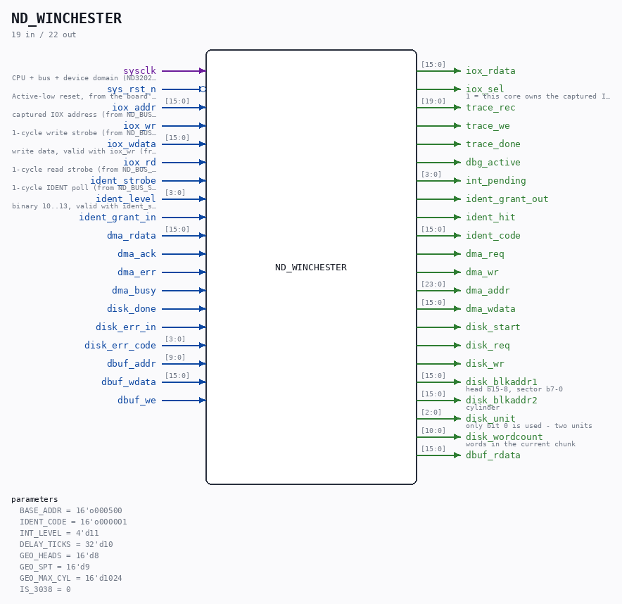
Schematic
Drawn from the Verilog: the yosys netlist of the Tang Nano 20K build, instance CORE.gen_wd.WD_500. Sub-modules are boxes (click the picture to open it full size; there every sub-module box links to its page, and every wire shows its Verilog name).
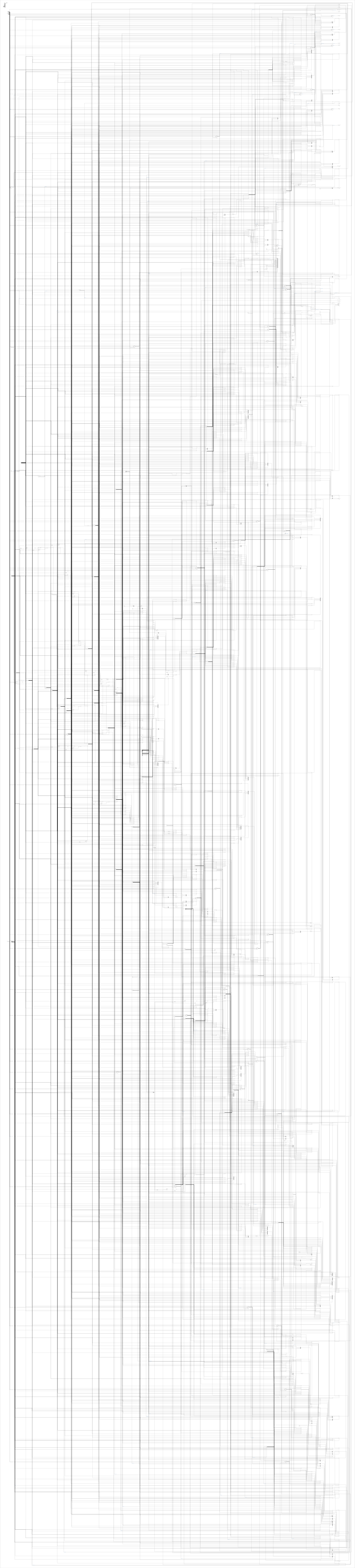
Parameters
| Parameter | Default |
|---|---|
BASE_ADDR |
16'o000500 |
IDENT_CODE |
16'o000001 |
INT_LEVEL |
4'd11 |
DELAY_TICKS |
32'd10 |
GEO_HEADS |
16'd8 |
GEO_SPT |
16'd9 |
GEO_MAX_CYL |
16'd1024 |
IS_3038 |
0 |
Ports
| Direction | Width | Name | Description |
|---|---|---|---|
| input | 1 |
sysclk |
CPU + bus + device domain (ND3202D sysclk/CLOCK_1/CLOCK_2) (from ND120_CORE.clk_cpu) |
| input | 1 |
sys_rst_n (active low) |
Active-low reset, from the board's power-on reset (from ND120_CORE.sys_rst_n) |
| input | [15:0] |
iox_addr |
captured IOX address (from ND_BUS_SLAVE.iox_addr) |
| input | 1 |
iox_wr |
1-cycle write strobe (from ND_BUS_SLAVE.iox_wr) |
| input | [15:0] |
iox_wdata |
write data, valid with iox_wr (from ND_BUS_SLAVE.iox_wdata) |
| input | 1 |
iox_rd |
1-cycle read strobe (from ND_BUS_SLAVE.iox_rd) |
| output | [15:0] |
iox_rdata |
|
| output | 1 |
iox_sel |
1 = this core owns the captured IOX address |
| output | [19:0] |
trace_rec |
|
| output | 1 |
trace_we |
|
| output | 1 |
trace_done |
|
| output | 1 |
dbg_active |
|
| output | [3:0] |
int_pending |
|
| input | 1 |
ident_strobe |
1-cycle IDENT poll (from ND_BUS_SLAVE.ident_strobe) |
| input | [3:0] |
ident_level |
binary 10..13, valid with ident_strobe (from ND_BUS_SLAVE.ident_level) |
| input | 1 |
ident_grant_in |
|
| output | 1 |
ident_grant_out |
|
| output | 1 |
ident_hit |
|
| output | [15:0] |
ident_code |
|
| output | 1 |
dma_req |
|
| output | 1 |
dma_wr |
|
| output | [23:0] |
dma_addr |
|
| output | [15:0] |
dma_wdata |
|
| input | [15:0] |
dma_rdata |
|
| input | 1 |
dma_ack |
|
| input | 1 |
dma_err |
|
| input | 1 |
dma_busy |
|
| output | 1 |
disk_start |
|
| output | 1 |
disk_req |
|
| output | 1 |
disk_wr |
|
| output | [15:0] |
disk_blkaddr1 |
head b15-8, sector b7-0 |
| output | [15:0] |
disk_blkaddr2 |
cylinder |
| output | [2:0] |
disk_unit |
only bit 0 is used - two units |
| output | [10:0] |
disk_wordcount |
words in the current chunk |
| input | 1 |
disk_done |
|
| input | 1 |
disk_err_in |
|
| input | [3:0] |
disk_err_code |
|
| input | [9:0] |
dbuf_addr |
|
| input | [15:0] |
dbuf_wdata |
|
| input | 1 |
dbuf_we |
|
| output | [15:0] |
dbuf_rdata |
Verilog source
Verilog/ND-BUS-DEVICES/WINCHESTER/circuit/ND_WINCHESTER.v on GitHub.
Show the Verilog of ND_WINCHESTER (1144 lines)
`include "nd_storage_status.vh"
/**************************************************************************
** ND WINCHESTER DISC CONTROLLER, 5 1/4 inch ST506 (3041) / 8 inch (3038) **
** **
** DMA block device, IOX 500-507, ident 1, interrupt level 11. **
** **
** Register core made 1:1 faithful to two host-gated C implementations **
** that are themselves proven byte-identical against each other: **
** nd100x src/devices/winchester/deviceWinchester.c (synchronous) **
** portable lib/NDDeviceCore/src/nd_winchester.c (phase machine) **
** A shared conformance sequence drives both and the traces are diffed; **
** this RTL follows the same decisions. Primary source for every rule **
** below is ND-11.015.01, sections 2.1 and 3.1-3.5 plus 4.1. **
** **
** ---------------------------------------------------------------------- **
** WHY THIS CARD EXISTS ALONGSIDE ND_SMD.v **
** **
** The families differ in how the 24-bit memory address and the word **
** count are loaded, and that is what tells them apart: **
** **
** NORD-10 large disc address ONE access, word count ONE access **
** ECC (ND 558/559) address ONE access, word count ONE access **
** 15 MHz SMD (ND 632) address TWO accesses, word count TWO accesses **
** Winchester (this) address TWO accesses, word count ONE access **
** **
** The ND-120's own MASS STORAGE LOAD microcode (PROM listing, CSA **
** 002221-002227) writes the core address TWICE and the word count ONCE. **
** That is the Winchester pattern exactly - which is why this core needs **
** NO boot-mode special case at all. ND_SMD.v carries one (s_boot_mode, **
** the BPUN byte-server plus the "a +1 or +7 write leaves boot mode" **
** escape) precisely because the microcode's protocol does NOT match its **
** registers. Here the microcode drives the normal register path and a **
** normal GO, so there is nothing to special-case. **
** **
** There is also NO register multiplex bit (no CWR): every IOX offset **
** means exactly one thing, and there is no controller-type strap - the **
** loading protocol is fixed. **
** **
** Register map (offset from base, sec 3.1): **
** +0 R Read memory address LO 16 first, then HI 8 **
** +1 W Load memory address HI 8 first, then LO 16 **
** +2 R NOT USED - reads 0 ("IOX 502 Not used" in the sec 3.1 table) **
** +3 W Load block address cylinder b15-5, sector b4-0 **
** +4 R Read status register READING IT RESETS THE FLIP-FLOPS **
** +5 W Load control word GO / opcode **
** +6 R Read block address unconditional - the sec 3.1 table has **
** no test-mode qualifier **
** +7 W Load word count / step count SINGLE access **
** **
** NOTE the deliberate asymmetry at +0/+1: address WRITES go HI then LO, **
** address READS come back LO then HI (sec 3.2). **
** **
** The upper/lower selection flip-flop is reset by ANY of four events **
** (sec 3.2), all four implemented here: master clear, programmed device **
** clear (control b4), a status register read, and activation (b2). **
** **
** Control word (+5, sec 3.4): **
** b0 int-enable (on NOT active), b1 error-int enable, b2 ACTIVE (GO), **
** b3 test mode, b4 device clear, b5-8 head, b9 unit (ONE bit - hence **
** two units maximum), b10 unused, b11-13 operation M0..M7, **
** b14 seek direction (ZERO = towards cylinder 0), b15 bad track. **
** **
** Status (+4, sec 3.5): **
** b0 int-enabled b1 error-int-enabled b2 active **
** b3 finished with a device operation b4 inclusive OR (b5-13)**
** b5 3041: r/w during RTZ b6 timeout b7 disk fault **
** b8 address mismatch b9 CRC error b10 compare error **
** b11 FIFO over/under-run or DMA channel error **
** b12 always 0 b13 3041: always 1 / 3038: r/w gate active **
** b14 on cylinder b15 always 0 - distinguishes this card from **
** the 10 Mb controller **
** **
** INTERRUPT (sec 4.1), the rule TPE CONFIGURATION probes with: **
** "If the controller is ready for an operation (status bit 3 = 1), **
** and interrupt is enabled (status bit 0 has been set by control bit **
** 0 = 1), the interrupt signal BINT11 will be active ... The IDENT **
** code may now be read by an IDENT PL11 instruction." **
** A CONDITION on the current status, not a pulse: activation drops **
** b3 and therefore drops the line, which returns at completion. The C **
** port shipped once without this and TPE reported "No identcode found **
** on level 11D, expected identcode : 1B". **
** **
** HARDWARE-CONSTRAINED DIVERGENCE, same as ND_SMD.v: the C models **
** pre-check that a unit is ATTACHED and (for writes) not WRITE- **
** PROTECTED using media metadata. This core has no backend metadata **
** port, so those two faults arrive as disk_err_in during the transfer **
** and become the same terminated-with-error result. The address- **
** mismatch bound (b8) IS pre-checked against the GEO_* parameters. **
** **
** MEDIA FILES: this card's images are WDn.IMG, NEVER SMDn.IMG. **
** **
** Thumbwheels (both level 11, sec 3.1): **
** tw0 disk system 1, base 00500 ident 001 **
** tw1 disk system 2, base 00510 ident 005 **
** 500-507 is the SAME block as the CDC cartridge disc - a machine has **
** one card or the other, never both. **
** **
** Ronny Hansen **
***************************************************************************/
module ND_WINCHESTER #(
parameter [15:0] BASE_ADDR = 16'o000500,
parameter [15:0] IDENT_CODE = 16'o000001,
parameter [3:0] INT_LEVEL = 4'd11,
// How long the controller stays ACTIVE after a GO before it reports
// completion, in sysclk cycles. Do NOT set this by hand at an
// instantiation: it is a TIME, so the board wrapper computes it from its
// own clock frequency. The module default stays small so the unit
// testbenches run fast. Same rule as ND_SMD.v's DELAY_TICKS.
parameter [31:0] DELAY_TICKS = 32'd10,
// Geometry for the address-mismatch bound. Default = the Micropolis 1325
// (the DISC-74-1): 8 heads, 9 sectors/track, 1024 cylinders, 1024-byte
// sectors. That is the drive SINTRAN boots from, and the default both C
// implementations use. A backend owning a different drive passes its own.
parameter [15:0] GEO_HEADS = 16'd8,
parameter [15:0] GEO_SPT = 16'd9,
parameter [15:0] GEO_MAX_CYL = 16'd1024,
// Card model. 0 = 3041 (5 1/4 inch ST506), whose status b13 reads a
// constant 1; 1 = 3038 (8 inch), whose b13 is the live read/write gate.
// A parameter rather than an input for the same reason as ND_SMD.v's
// strap: an unwired input floats and would read as 0 anyway.
parameter IS_3038 = 0
) (
input wire sysclk, //! CPU + bus + device domain (ND3202D sysclk/CLOCK_1/CLOCK_2) (from ND120_CORE.clk_cpu)
input wire sys_rst_n, //! Active-low reset, from the board's power-on reset (from ND120_CORE.sys_rst_n)
// Device bus (from ND_BUS_SLAVE) - IOX slave side
input wire [15:0] iox_addr, //! captured IOX address (from ND_BUS_SLAVE.iox_addr)
input wire iox_wr, //! 1-cycle write strobe (from ND_BUS_SLAVE.iox_wr)
input wire [15:0] iox_wdata, //! write data, valid with iox_wr (from ND_BUS_SLAVE.iox_wdata)
input wire iox_rd, //! 1-cycle read strobe (from ND_BUS_SLAVE.iox_rd)
output reg [15:0] iox_rdata,
output wire iox_sel, // 1 = this core owns the captured IOX address
// ---- on-silicon IOX trace tap -------------------------------------
// One record per COMPLETED IOX access to this card:
// {rw, reg[2:0], data[15:0]}, rw 1 = write (data is iox_wdata),
// rw 0 = read (data is what we returned).
// Costs nothing when the consumer ties it off - synthesis prunes it.
// This exists because ND_WINCHESTER.v is byte-for-byte conformant with
// the nd100x C model across the whole DISC-TEMA "DU-DI-C" IOX trace and
// the fault still only appears on silicon, so the sequence the CPU
// actually issues is the one piece of evidence nobody has. ND_SMD.v had
// the equivalent (ND120_SMD_TRACE) and that is what made it tractable.
output wire [19:0] trace_rec,
output wire trace_we,
// Pulses when a device operation COMPLETES (the FinishOperation point).
// A capture trigger needs this: "the card went quiet" is not enough on
// its own, because the card is also quiet for many seconds while the
// diagnostic collects its prompts from the operator.
output reg trace_done,
//! DEBUG (24-AUG-2026): the controller-active flag, for the stage timer
//! that measures WHERE a disc operation's ~1 s actually goes.
output wire dbg_active,
output wire [3:0] int_pending,
input wire ident_strobe, //! 1-cycle IDENT poll (from ND_BUS_SLAVE.ident_strobe)
input wire [3:0] ident_level, //! binary 10..13, valid with ident_strobe (from ND_BUS_SLAVE.ident_level)
input wire ident_grant_in,
output wire ident_grant_out,
output wire ident_hit,
output wire [15:0] ident_code,
// DMA master client port (to ND_DMA_MASTER)
output reg dma_req,
output reg dma_wr,
output reg [23:0] dma_addr,
output reg [15:0] dma_wdata,
input wire [15:0] dma_rdata,
input wire dma_ack,
input wire dma_err,
input wire dma_busy,
// Disk backend: chunk transfers through the internal buffer. Same port
// shape as ND_SMD.v so the nd_storage adapter pattern carries over; the
// block address is split into the two words the adapter expects.
output reg disk_start,
output reg disk_req,
output reg disk_wr,
output wire [15:0] disk_blkaddr1, // head b15-8, sector b7-0
output wire [15:0] disk_blkaddr2, // cylinder
output wire [2:0] disk_unit, // only bit 0 is used - two units
output wire [10:0] disk_wordcount, // words in the current chunk
input wire disk_done,
input wire disk_err_in,
// WHY the backend failed (nd_storage_status.vh), valid with disk_done.
// Mapped below onto the status bits ND-11.015.01 sec 3.5 ALREADY
// defines for this card - no new status bit is invented here. Before
// this existed every backend failure became a CRC error, so "no SD
// card", "WD0.IMG is not on the card" and "block past the end of the
// image" were one indistinguishable bit at the guest.
input wire [3:0] disk_err_code,
input wire [9:0] dbuf_addr,
input wire [15:0] dbuf_wdata,
input wire dbuf_we,
output reg [15:0] dbuf_rdata
);
localparam [10:0] BUF_WORDS = 11'd1024;
// Device operation codes, control word b11-13 (sec 3.4).
localparam [2:0] OP_READ = 3'd0; // M0
localparam [2:0] OP_WRITE = 3'd1; // M1
localparam [2:0] OP_READ_PAR = 3'd2; // M2
localparam [2:0] OP_COMPARE = 3'd3; // M3
localparam [2:0] OP_SEEK = 3'd4; // M4 - step count in +7
localparam [2:0] OP_WR_FORMAT = 3'd5; // M5
localparam [2:0] OP_LOAD_CTRL = 3'd6; // M6 - 3038 only, NOT activated
localparam [2:0] OP_RTZ = 3'd7; // M7
// ---- controller registers ----
reg [15:0] s_mem_addr_lo; // memory address bits 0-15
reg [7:0] s_mem_addr_hi; // memory address bits 16-23
reg [15:0] s_word_cnt; // word count, ALSO the M4 step count
reg [15:0] s_blkaddr; // cylinder b15-5, sector b4-0
wire [10:0] w_cyl = s_blkaddr[15:5];
wire [4:0] w_sector = s_blkaddr[4:0];
// ---- unit selection + per-unit state ----
reg s_sel_unit; // control word b9 - ONE bit, two units
reg [3:0] s_head; // control word b5-8
reg s_seek_dir; // control word b14: 0 = towards cylinder 0
reg s_bad_track; // control word b15
reg [1:0] s_on_cyl; // per-unit on-cylinder (status b14)
// M4 is a RELATIVE STEP seek, so each arm's position must be remembered.
reg [15:0] s_cyl_pos [0:1];
// ---- status flags (sec 3.5) ----
reg s_int_en; // b0
reg s_errint_en; // b1
reg s_active; // b2
assign dbg_active = s_active;
reg s_rft; // b3 finished with a device operation
reg s_rtz_viol; // b5
reg s_time_out; // b6
reg s_disk_fault; // b7
reg s_addr_mismatch; // b8
reg s_crc_err; // b9
reg s_compare_err; // b10
reg s_dma_ch_err; // b11
reg s_rw_gate; // b13 on the 3038 only
reg s_test_mode; // control b3
// ---- the upper/lower selection flip-flops (sec 3.2) ----
`ifdef ND120_WD_TRACE
reg [31:0] s_trace_cyc; // sysclk counter for the simulation-only trace
`endif
reg s_ma_write_ff;
reg s_ma_read_ff;
reg s_irq; // latched level-11 interrupt line
assign disk_blkaddr1 = {4'd0, s_head, 3'd0, w_sector};
assign disk_blkaddr2 = {5'd0, w_cyl};
assign disk_unit = {2'd0, s_sel_unit};
// ---- internal buffer ----
// Async-read arrays do NOT map to Gowin BSRAM, so this is a simple dual-port
// RAM: one muxed write port, one registered read port whose address follows
// the active consumer. Same refactor as ND_SMD.v and ND_FLOPPY_DMA.
reg [15:0] s_buffer[0:1023];
// ---- decode ----
wire s_addressed = (iox_addr[15:3] == BASE_ADDR[15:3]);
assign iox_sel = s_addressed;
wire [2:0] s_reg = iox_addr[2:0];
wire s_wr_here = iox_wr && s_addressed;
wire s_rd_here = iox_rd && s_addressed;
// SIDE EFFECTS MUST BE EDGE-TRIGGERED, NOT LEVEL-TRIGGERED - AND THE READ
// ALTERNATOR MUST ADVANCE AT THE END OF THE ACCESS, NOT THE START.
//
// iox_rd / iox_wr are held for the whole ND-BUS I/O cycle, which is many
// sysclk periods - the bus runs at the original ND speed while the card is
// clocked by sysclk. Two separate faults came out of using the level:
//
// 1. Every non-idempotent side effect fired once PER SYSCLK for the
// duration of the access. The +0 read alternator (s_ma_read_ff) and
// the +1 write alternator (s_ma_write_ff) toggled N times instead of
// once, so which half of the memory address register you got depended
// on how many clocks the bus cycle happened to last.
//
// 2. Even toggled exactly once, toggling at the START of a read changes
// iox_rdata WHILE the bus is still sampling it: the master sees the
// other half. The alternator therefore advances on the END of the
// access (s_rd_end), so the selected half is stable for the whole
// cycle and the NEXT read gets the other one. The register offset is
// latched with it, because iox_addr may already have moved on.
//
// Symptom on silicon (05-AUG-2026): DISC-TEMA J02 "DU-DI-C" on
// DISC-74MB-1 returned all 512 data words correctly and the identical
// status word 060010, then reported "Memory address Register not as
// expected" - the two IOX 500 reads came back swapped. Reproduced against
// the nd100x trace in nd_winchester_oracle_tb.v.
//
// Writes keep the RISING edge: iox_wdata is stable when the strobe goes
// active, and a write has no read-data to hold steady.
reg s_iox_rd_q, s_iox_wr_q;
reg [2:0] s_reg_q;
always @(posedge sysclk or negedge sys_rst_n) begin
if (!sys_rst_n) begin
s_iox_rd_q <= 1'b0;
s_iox_wr_q <= 1'b0;
s_reg_q <= 3'd0;
end else begin
s_iox_rd_q <= s_rd_here;
s_iox_wr_q <= iox_wr;
if (s_rd_here) s_reg_q <= s_reg;
end
end
wire s_rd_end = s_iox_rd_q && !s_rd_here; // end of an addressed read
wire s_wr_edge = s_wr_here && !s_iox_wr_q;
// Trace record encoding. {rw, reg} is the top nibble; 0-7 = a READ of
// +0..+7, 8-F = a WRITE to +0..+7. Two of those 16 codes are impossible on
// this card and are reused for events that are NOT IOX at all but that
// software can see just as clearly:
//
// 8xxxx IDENT answered on level 11, xxxx = the code returned
// Axxxx the interrupt line CHANGED, xxxx = 1 raised / 0 dropped
//
// (+0 and +2 are read-only, so "write to +0" and "write to +2" can never
// occur.) They are here because the IOX sequence on silicon now matches the
// nd100x C model access for access and DISC-TEMA still disagrees with it,
// so whatever decides the verdict is something an IOX trace cannot show.
reg s_irq_q;
always @(posedge sysclk or negedge sys_rst_n) begin
if (!sys_rst_n) s_irq_q <= 1'b0;
else s_irq_q <= s_irq;
end
wire s_irq_edge = (s_irq != s_irq_q);
// Cxxxx an IOX to an address that is NOT ours, xxxx = that address.
// The card sees the whole bus, so this answers "where is the CPU actually
// going" - the question left open when a mass-storage load (20500&) hangs
// having touched this card fewer than four times. If the microcode is
// driving 20501/20503/20507 because bit 13 was never stripped from the
// typed load code, nothing decodes, the bus times out, and the CPU hangs
// exactly as observed. ND_SMD.v has the same idea under [SMD-OTHER].
reg s_foreign_q;
wire s_foreign = (iox_rd || iox_wr) && !s_addressed;
always @(posedge sysclk or negedge sys_rst_n) begin
if (!sys_rst_n) s_foreign_q <= 1'b0;
else s_foreign_q <= s_foreign;
end
wire s_foreign_edge = s_foreign && !s_foreign_q;
// An IDENT cycle this card did NOT answer is recorded too (tag 9). Without
// it the trace cannot tell the two ways an interrupt goes unclaimed apart,
// and on 09-AUG-2026 a silicon capture of the File System Investigator hit
// exactly that wall: the irq line rose (tag A) and no tag 8 ever followed,
// which is equally consistent with "the CPU never ran an IDENT cycle at all"
// and with "it did, but a device ahead of this one in the grant chain took
// it" - the floppy is also level 11 and sits earlier in the chain. Tag 9
// carries grant_in and s_irq, so the answer is read straight off the dump:
// no tag 9 at all -> the CPU never identified; look CPU-side.
// tag 9 with grant=0 -> the grant never arrived; a device ahead consumed it.
// tag 9 with grant=1,
// irq=0 -> our own irq had already dropped before the cycle.
reg s_idstb_q;
always @(posedge sysclk or negedge sys_rst_n) begin
if (!sys_rst_n) s_idstb_q <= 1'b0;
else s_idstb_q <= ident_strobe;
end
wire s_idstb_edge = ident_strobe && !s_idstb_q &&
(ident_level == INT_LEVEL) && !s_ident_answer;
assign trace_we = s_wr_edge || (s_rd_here && !s_iox_rd_q)
|| s_ident_answer || s_idstb_edge || s_irq_edge
|| s_foreign_edge;
assign trace_rec = s_wr_edge ? {1'b1, s_reg, iox_wdata}
: (s_rd_here && !s_iox_rd_q) ? {1'b0, s_reg, iox_rdata}
: s_ident_answer ? {4'h8, IDENT_CODE}
: s_idstb_edge ? {4'h9, 10'd0, ident_grant_in, s_irq,
ident_level}
: s_irq_edge ? {4'hA, 15'd0, s_irq}
: {4'hC, iox_addr};
// ---- status assembly (sec 3.5) ----
// Bit 4 is the inclusive OR of the error bits. Bit 13 is EXCLUDED even
// though the manual's wording says "bits 5-13": on a 3041 b13 is always 1,
// so including it would make the error OR permanently set.
wire s_incl_or = s_rtz_viol | s_time_out | s_disk_fault | s_addr_mismatch |
s_crc_err | s_compare_err | s_dma_ch_err;
// Bit 13 is the card identity: the 3041 always reads 1 ("Used to distinguish
// the 3038 from the 3041"), the 3038 reports its live read/write gate.
wire s_contr_id = IS_3038 ? s_rw_gate : 1'b1;
wire [15:0] s_status =
{ 1'b0, // b15 always 0 - not the 10 Mb controller
s_on_cyl[s_sel_unit], // b14 on cylinder
s_contr_id, // b13 card identity
1'b0, // b12 always 0
s_dma_ch_err, // b11 FIFO over/under-run or DMA channel error
s_compare_err, // b10 compare error
s_crc_err, // b9 CRC error
s_addr_mismatch, // b8 address mismatch
s_disk_fault, // b7 disk fault or missing clocks
s_time_out, // b6 timeout
s_rtz_viol, // b5 r/w attempted during RTZ (3041)
s_incl_or, // b4 inclusive OR of b5-13
s_rft, // b3 finished with a device operation
s_active, // b2 controller active
s_errint_en, // b1 error interrupt enabled
s_int_en }; // b0 controller-not-active interrupt enabled
// ---- interrupt / ident (latched line) ----
assign int_pending = {(INT_LEVEL == 4'd13) && s_irq,
(INT_LEVEL == 4'd12) && s_irq,
(INT_LEVEL == 4'd11) && s_irq,
(INT_LEVEL == 4'd10) && s_irq};
wire s_ident_answer = ident_strobe && ident_grant_in &&
(ident_level == INT_LEVEL) && s_irq;
assign ident_hit = s_ident_answer;
assign ident_code = s_ident_answer ? IDENT_CODE : 16'd0;
assign ident_grant_out = ident_grant_in && !s_ident_answer;
// ---- IOX read mux ----
// Reads are NOT gated on a selected unit. These are CONTROLLER registers -
// they exist whether or not a drive is selected, and a probe must be able to
// tell an absent card from an idle one. Both C implementations shipped a
// "return 0 when no disk selected" gate here; it was a bug in all of them.
always @(*) begin
iox_rdata = 16'd0;
if (s_rd_here) begin
case (s_reg)
// Sec 3.2: the reads are the OPPOSITE order to the writes - the first
// IOX 500 returns the LOW 16 bits, the second the UPPER 8.
3'd0: iox_rdata = s_ma_read_ff ? {8'd0, s_mem_addr_hi} : s_mem_addr_lo;
// +2: "IOX 502 Not used" in the sec 3.1 table. There is no
// programmer-visible sector counter on this card - the sector counters
// named in the hardware description are internal. Both C models had a
// readable counter here until the cross-check sent us to the table.
3'd2: iox_rdata = 16'd0;
3'd4: iox_rdata = s_status;
// +6: "IOX 506 Read Block (disk) address register", with NO test-mode
// qualifier, so it reads back unconditionally.
3'd6: iox_rdata = s_blkaddr;
default: iox_rdata = 16'd0; // +1/+3/+5/+7 are write-only
endcase
end
end
// ---- transfer engine ----
localparam E_IDLE = 3'd0;
localparam E_DISK_RD = 3'd1; // backend: image chunk -> buffer
localparam E_MEM_WR = 3'd2; // DMA: buffer -> ND memory
localparam E_MEM_RD = 3'd3; // DMA: ND memory -> buffer
localparam E_DISK_WR = 3'd4; // backend: buffer -> image chunk
localparam E_DELAY = 3'd5; // completion delay -> FinishOperation
localparam E_MEM_CMP = 3'd6; // DMA: ND memory vs buffer (M3 compare)
reg [2:0] s_eng;
reg s_is_cmp; // this operation is M3, not M0
reg [10:0] s_chunk_q;
reg [10:0] s_sec_idx;
reg [31:0] s_delay_cnt;
reg s_dma_wait;
reg [23:0] s_dma_addr_r; // running ND word address
reg [23:0] s_words_left; // words still to move
reg s_unit; // selected drive for this command
assign disk_wordcount = s_chunk_q;
// CHS -> LBA, the same formula the SMD core and both C models use.
function [31:0] chs2lba;
input [15:0] cyl;
input [15:0] head;
input [15:0] sector;
begin
chs2lba = (({16'd0, cyl} * {16'd0, GEO_HEADS}) + {16'd0, head})
* {16'd0, GEO_SPT} + {16'd0, sector};
end
endfunction
// GO-time address decode (registers are stable outside a control write).
wire [31:0] w_lba = chs2lba({5'd0, w_cyl}, {12'd0, s_head}, {11'd0, w_sector});
wire [31:0] w_max_lba = chs2lba(GEO_MAX_CYL, GEO_HEADS, GEO_SPT);
wire [23:0] w_words = {8'd0, s_word_cnt};
task dma_issue(input wr, input [23:0] a, input [15:0] d);
begin
dma_req <= 1'b1;
dma_wr <= wr;
dma_addr <= a;
dma_wdata <= d;
s_dma_wait <= 1'b1;
end
endtask
// The four flip-flop reset conditions all call this (sec 3.2).
task clr_ff;
begin
s_ma_write_ff <= 1'b0;
s_ma_read_ff <= 1'b0;
end
endtask
// Terminate an operation in error. The specific status bit is set by the
// caller first. The operation still FINISHES (b3 goes to 1) because the
// manual's b3 is "finished with a device operation", not "finished
// successfully" - and because leaving b3 low would wedge a guest waiting on
// an interrupt that the sec 4.1 condition can then never produce.
task err_active;
begin
s_active <= 1'b0;
s_rft <= 1'b1;
trace_done <= 1'b1;
clr_ff;
// A FinishOperation, so the registers are left in their end-of-transfer
// state exactly as on the clean path (wd_sync_registers in both C
// models): the address advanced by the words that DID move, count zero.
s_mem_addr_lo <= s_dma_addr_r[15:0];
s_mem_addr_hi <= s_dma_addr_r[23:16];
s_word_cnt <= 16'd0;
s_on_cyl[s_unit] <= 1'b0;
s_eng <= E_IDLE;
s_dma_wait <= 1'b0;
if (s_errint_en) s_irq <= 1'b1;
else s_irq <= s_int_en; // sec 4.1: ready && enabled
end
endtask
// ==== BACKEND FAILURE -> STATUS BIT =====================================
//
// WHERE THESE BITS COME FROM: every bit set below is one the WINCHESTER
// CONTROLLER MANUAL ND-11.015.01, SECTION 3.5 (status register, IOX +4)
// already defines for this card. They are listed verbatim in this file's
// header block under "Status (+4, sec 3.5)" and assembled into s_status
// further down. NOTHING here is invented: this task chooses AMONG the
// manual's bits, it never adds one, never repurposes one, and never puts
// the reason code itself anywhere the guest can read it. That is the rule
// in Verilog/SD-FAT/circuit/nd_storage_status.vh - the storage stack is
// clean-room and may carry a reason code, a reproduced ND card may not.
//
// WHERE THE REASON CODE COMES FROM: nd_storage_engine.v tags the failure
// at the point it happens (card timeout, CMD17/CMD24 failure, no mount,
// block past end of file, broken FAT chain, engine watchdog), the code
// travels engine -> nd_storage -> nd_storage_disc_adapter (the Winchester
// reuses it at ST506 geometry) -> disk_err_code here.
//
// FULL MAPPING - all nine codes of nd_storage_status.vh:
//
// NDS_ERR_NOCARD b7 disk fault / missing clocks. No SD card in the
// slot: from the guest's side the drive is simply
// not usable, which is exactly what b7 means.
// NDS_ERR_NOTOPEN b7 same bit: WD0.IMG is not on the card (or its
// mount failed), so again there is no usable
// drive behind the interface.
// NDS_ERR_RANGE b8 address mismatch. The manual's b8 is "the
// address searched for was not found on the
// drive", which is precisely a block past the end
// of the image.
// NDS_ERR_TIMEOUT b6 timeout. The engine watchdog fired: the backend
// never answered - the same event b6 exists for.
// NDS_ERR_CARDIO b9 CRC error. The card answered but the data is
// not trustworthy (CMD17/CMD24 error, CRC, card
// stopped mid-block). b9 is this card's
// data-unreadable bit.
// NDS_ERR_FATCHAIN b9 same bit: the FAT chain is broken or circular,
// so the medium cannot yield the requested data.
// NDS_ERR_WRPROT b9 this card has NO write-protect bit in sec 3.5.
// NDS_ERR_WRALIGN b9 A refused write IS a failure to write the
// medium, so it lands on the general media-fault
// bit. The exact reason stays readable on the
// storage seam (WDISK_ERR_CODE) for a testbench
// or a probe - it is only the GUEST that cannot
// tell these two apart, and that is the manual's
// limitation, not a shortcut taken here.
// NDS_ERR_NONE never reaches this task (no error, no call).
//
// b4 (inclusive OR of b5-b13) follows automatically from s_incl_or, so
// any bit chosen here also raises the guest's "something went wrong" bit
// exactly as the manual specifies.
//
// WHY THIS EXISTS: before it, both call sites hard-coded ONE bit, so
// "no SD card", "WD0.IMG missing", "block past the end of the image",
// "broken FAT chain" and "the card stopped answering" were a single
// indistinguishable CRC error at the guest, at the console and in a
// waveform. That is what made the 08-AUG-2026 zero-read investigation as
// long as it was.
// ========================================================================
task set_backend_fault;
input [3:0] code;
begin
case (code)
// b7 disk fault / missing clocks (sec 3.5)
`NDS_ERR_NOCARD,
`NDS_ERR_NOTOPEN: s_disk_fault <= 1'b1;
// b8 address mismatch (sec 3.5)
`NDS_ERR_RANGE: s_addr_mismatch <= 1'b1;
// b6 timeout (sec 3.5)
`NDS_ERR_TIMEOUT: s_time_out <= 1'b1;
// b9 CRC error (sec 3.5) - CARDIO, FATCHAIN, WRPROT, WRALIGN
default: s_crc_err <= 1'b1;
endcase
end
endtask
// ---- buffer RAM ports (BSRAM-mappable: sync write + sync read) ----------
wire s_memrd_commit = (s_eng == E_MEM_RD) && s_dma_wait &&
dma_ack && !dma_err;
wire s_buf_we = dbuf_we | s_memrd_commit;
wire [ 9:0] s_buf_waddr = dbuf_we ? dbuf_addr : s_sec_idx[9:0];
wire [15:0] s_buf_wdata = dbuf_we ? dbuf_wdata : dma_rdata;
wire [ 9:0] s_buf_raddr = (s_eng == E_MEM_WR) ? s_sec_idx[9:0] :
(s_eng == E_MEM_CMP) ? s_sec_idx[9:0] :
(s_eng == E_DISK_WR) ? dbuf_addr :
10'd0;
reg [15:0] s_buf_dout;
reg [ 9:0] s_buf_raddr_q;
wire s_buf_valid = (s_buf_raddr_q == s_buf_raddr);
always @(posedge sysclk) begin
if (s_buf_we) s_buffer[s_buf_waddr] <= s_buf_wdata;
s_buf_dout <= s_buffer[s_buf_raddr];
s_buf_raddr_q <= s_buf_raddr;
end
always @(*) dbuf_rdata = s_buf_dout;
always @(posedge sysclk or negedge sys_rst_n) begin
if (!sys_rst_n) begin
s_mem_addr_lo <= 16'd0;
s_mem_addr_hi <= 8'd0;
s_word_cnt <= 16'd0;
s_blkaddr <= 16'd0;
s_sel_unit <= 1'b0;
s_head <= 4'd0;
s_seek_dir <= 1'b0;
s_bad_track <= 1'b0;
s_on_cyl <= 2'd0;
s_cyl_pos[0] <= 16'd0;
s_cyl_pos[1] <= 16'd0;
s_int_en <= 1'b0;
s_errint_en <= 1'b0;
s_active <= 1'b0;
s_rft <= 1'b0;
s_rtz_viol <= 1'b0;
s_time_out <= 1'b0;
s_disk_fault <= 1'b0;
s_addr_mismatch<= 1'b0;
s_crc_err <= 1'b0;
s_compare_err <= 1'b0;
s_dma_ch_err <= 1'b0;
s_rw_gate <= 1'b0;
s_test_mode <= 1'b0;
`ifdef ND120_WD_TRACE
s_trace_cyc <= 32'd0;
`endif
trace_done <= 1'b0;
s_ma_write_ff <= 1'b0; // master clear is reset condition #1 (sec 3.2)
s_ma_read_ff <= 1'b0;
s_irq <= 1'b0;
s_eng <= E_IDLE;
s_is_cmp <= 1'b0;
s_chunk_q <= 11'd0;
s_sec_idx <= 11'd0;
s_delay_cnt <= 32'd0;
s_dma_wait <= 1'b0;
s_dma_addr_r <= 24'd0;
s_words_left <= 24'd0;
s_unit <= 1'b0;
dma_req <= 1'b0;
dma_wr <= 1'b0;
dma_addr <= 24'd0;
dma_wdata <= 16'd0;
disk_start <= 1'b0;
disk_req <= 1'b0;
disk_wr <= 1'b0;
end else begin
dma_req <= 1'b0;
disk_start <= 1'b0;
disk_req <= 1'b0;
trace_done <= 1'b0;
// ---- read-strobe side effects (END of access: see the note above) ----
if (s_rd_end) begin
case (s_reg_q)
// Successive +0 reads alternate LO then HI (sec 3.2).
3'd0: s_ma_read_ff <= ~s_ma_read_ff;
// A status read is flip-flop reset condition #3 (sec 3.2).
3'd4: clr_ff;
default: ;
endcase
end
// ---- IOX register writes (EDGE: see the note at s_wr_edge) ----
if (s_wr_edge) begin
case (s_reg)
// +1 Load memory address: TWO accesses, HI 8 then LO 16 (sec 3.2).
3'd1: begin
if (s_ma_write_ff) begin
s_mem_addr_lo <= iox_wdata; // second write: LO 16
s_ma_write_ff <= 1'b0;
end else begin
s_mem_addr_hi <= iox_wdata[7:0]; // first write: HI 8
s_ma_write_ff <= 1'b1;
end
end
// +3 Load block address: cylinder b15-5, sector b4-0 (sec 3.3).
3'd3: s_blkaddr <= iox_wdata;
// +5 Load control word (GO / opcode), sec 3.4.
3'd5: begin
s_int_en <= iox_wdata[0];
s_errint_en <= iox_wdata[1];
s_test_mode <= iox_wdata[3];
s_head <= iox_wdata[8:5];
s_sel_unit <= iox_wdata[9];
s_seek_dir <= iox_wdata[14];
s_bad_track <= iox_wdata[15];
// Device clear (b4). Sec 3.4: "To clear the disk drive, it may be
// necessary to execute two consecutive device clear before reading
// a correct status."
//
// Processed INLINE - it must NOT skip the ready/interrupt update
// below, because a single control word may carry device clear AND
// the interrupt enable together, which is how a probe usually
// opens. Both C models take the same shape, following the
// paper-tape reader's "processed inline, does NOT break".
if (iox_wdata[4]) begin
s_active <= 1'b0;
s_mem_addr_lo <= 16'd0;
s_mem_addr_hi <= 8'd0;
s_word_cnt <= 16'd0;
s_blkaddr <= 16'd0;
s_rtz_viol <= 1'b0;
s_time_out <= 1'b0;
s_disk_fault <= 1'b0;
s_addr_mismatch<= 1'b0;
s_crc_err <= 1'b0;
s_compare_err <= 1'b0;
s_dma_ch_err <= 1'b0;
clr_ff;
s_eng <= E_IDLE;
s_dma_wait <= 1'b0;
s_irq <= 1'b0;
end
// Activation (b2). Sec 3.4: every operation code is activated by
// loading the code with the activate bit, EXCEPT M6.
//
// M6 only sets additional control bits (3038 only) - it is a
// control-bit load, not an operation - so a control word carrying
// it takes the NON-activating path below and leaves the card
// ready. The manual never says what the hardware does if you
// activate M6 anyway ("no activation should be made" is guidance
// to the programmer); both C models make the same choice, and the
// cross-check trace keeps all three from drifting apart.
if (iox_wdata[2] && iox_wdata[13:11] != OP_LOAD_CTRL) begin
// Activation is flip-flop reset condition #4 (sec 3.2).
clr_ff;
s_active <= 1'b1;
s_rft <= 1'b0;
s_unit <= iox_wdata[9];
s_on_cyl[iox_wdata[9]] <= 1'b1;
s_rtz_viol <= 1'b0;
s_time_out <= 1'b0;
s_disk_fault <= 1'b0;
s_addr_mismatch <= 1'b0;
s_crc_err <= 1'b0;
s_compare_err <= 1'b0;
s_dma_ch_err <= 1'b0;
// Sec 4.1 is a condition on the CURRENT status: activation drops
// b3, so the line drops with it and returns at completion.
s_irq <= 1'b0;
s_dma_addr_r <= {s_mem_addr_hi, s_mem_addr_lo};
s_words_left <= w_words;
case (iox_wdata[13:11])
OP_SEEK: begin
// M4 is a RELATIVE STEP seek (sec 3.4.5): step count in the
// word-count register, direction in b14 where ZERO means
// towards cylinder 0. Clamped at both stops - running the
// arm past either one is not a status-reported error, the
// drive simply stops.
if (!iox_wdata[14]) begin
s_cyl_pos[iox_wdata[9]] <=
(s_cyl_pos[iox_wdata[9]] > s_word_cnt) ?
(s_cyl_pos[iox_wdata[9]] - s_word_cnt) : 16'd0;
end else begin
s_cyl_pos[iox_wdata[9]] <=
((s_cyl_pos[iox_wdata[9]] + s_word_cnt) > GEO_MAX_CYL ||
(s_cyl_pos[iox_wdata[9]] + s_word_cnt) <
s_cyl_pos[iox_wdata[9]]) ?
GEO_MAX_CYL : (s_cyl_pos[iox_wdata[9]] + s_word_cnt);
end
// A zero-step seek moves nothing: the drive only re-checks
// its position and completes. See the OP_RTZ note - the
// completion delay is only earned by ARM MOTION.
s_delay_cnt <= (s_word_cnt == 16'd0) ? 32'd8 : DELAY_TICKS;
s_eng <= E_DELAY;
end
OP_RTZ: begin
// EVERY RTZ earns DELAY_TICKS, including one whose arm is
// already at cylinder 0.
//
// 06-AUG-2026 this charged a fixed 8 ticks when the arm was
// already home, on the reasoning that a track-0 sensor check
// is not a seek and that the full delay desynced DISC-TEMA
// into reporting "Memory address Register not as expected".
// That was a workaround, and the symptom it worked around
// has since been root-caused elsewhere: the real fault was
// an IOX write zeroing the A register, fixed as the CDLBD
// 74646 pin-node correction in BIF_DPATH_9.v.
//
// The 8-tick path is itself a bug, and the nd100x oracle
// proves it. In oracle/fsi-lifi-nd100x.trace the File System
// Investigator writes 034005 and its next status read
// returns 060005 - ACTIVE, seek still running. On silicon
// the same read returns 060011, already finished, because
// 8 ticks at 6.75 MHz is 1.2 us and no guest can poll that
// fast. A real drive unloads and reseeks track 0 on every
// RTZ; it is never instantaneous. Measured by
// sim/nd_winchester_rtz_tb.v, which reproduces the silicon
// divergence and fails on the old 8-tick behaviour.
s_cyl_pos[iox_wdata[9]] <= 16'd0;
s_rtz_viol <= 1'b0;
s_delay_cnt <= DELAY_TICKS;
s_eng <= E_DELAY;
end
OP_READ, OP_WRITE, OP_COMPARE: begin
// Test mode bypasses the bounds check (sec 3.4).
if (!iox_wdata[3] &&
((w_lba > w_max_lba) ||
({11'd0, s_head} >= GEO_HEADS) ||
({11'd0, w_sector} >= GEO_SPT))) begin
s_addr_mismatch <= 1'b1;
s_active <= 1'b0;
s_rft <= 1'b1;
trace_done <= 1'b1;
s_on_cyl[iox_wdata[9]] <= 1'b0;
s_eng <= E_IDLE;
s_dma_wait <= 1'b0;
// EVERY completion is a FinishOperation, and a
// FinishOperation always clears the upper/lower selection
// flip-flops and zeroes the word counter - both C models
// route this path through wd_finish_operation(), which
// calls wd_clear_flipflops() + wd_sync_registers().
// Leaving them alone here is what made a LATER IOX 500
// read return the wrong half: the transfer and the status
// word stay perfectly correct, so the fault surfaces only
// as DISC-TEMA's "Memory address Register not as
// expected" long after the probe that caused it. The
// address registers themselves are NOT advanced - nothing
// was transferred, which is also what wd_sync_registers
// computes here (mem_addr still equals what was loaded).
clr_ff;
s_word_cnt <= 16'd0;
if (iox_wdata[1]) s_irq <= 1'b1;
else s_irq <= iox_wdata[0];
end else if (w_words != 24'd0) begin
s_chunk_q <= (w_words > {13'd0, BUF_WORDS}) ?
BUF_WORDS : w_words[10:0];
s_sec_idx <= 11'd0;
// M3 takes the READ path off the disc - it has to, it is
// reading the sector - and then compares in E_MEM_CMP
// instead of storing in E_MEM_WR.
s_is_cmp <= (iox_wdata[13:11] == OP_COMPARE);
if (iox_wdata[13:11] == OP_READ ||
iox_wdata[13:11] == OP_COMPARE) begin
disk_start <= 1'b1;
disk_req <= 1'b1;
disk_wr <= 1'b0;
s_eng <= E_DISK_RD;
end else begin
disk_start <= 1'b1;
s_eng <= E_MEM_RD;
end
end else begin
// A zero-length transfer still completes.
s_delay_cnt <= DELAY_TICKS;
s_eng <= E_DELAY;
end
end
default: begin
// M2 read-parity / M5 write-format: documented stubs,
// acknowledged as no-data completions so the guest proceeds.
//
// M3 COMPARE IS NO LONGER ONE OF THEM. It was, and the note
// here claimed that matched both C models - it does not.
// nd100x's deviceWinchester.c reads the sector, DMA-reads
// the same words back out of ND memory, compares them, and
// then writes the ADVANCED core address into the memory
// address register like any other transfer. The stub left
// that register holding the address the guest had loaded.
//
// SINTRAN reads +0 back after every operation, so the stub
// is visible to it. Measured 10-AUG-2026: booting WD0.IMG
// with '20500&', the Tang and nd100x request the SAME 124
// disc addresses and then split at exactly the group where
// SINTRAN reads block 0 twice and compares it. nd100x moves
// on; the Tang re-issued block 0 eleven times and gave up
// with SINTRAN's own 'TRANSFER ERROR' message.
s_delay_cnt <= DELAY_TICKS;
s_eng <= E_DELAY;
end
endcase
end else if (!iox_wdata[4]) begin
// A control word that does NOT activate (and is not a device
// clear, which handled its own interrupt above): the controller
// stays idle and is by definition ready for an operation, so
// status b3 goes to 1 and the sec 4.1 condition is re-evaluated.
// THIS is what makes TPE CONFIGURATION find the card.
//
// ONLY WHEN IT REALLY IS IDLE. "Stays idle" is a PREMISE, not a
// consequence, and it is one this RTL can violate where the C
// models cannot: their Wd_ExecuteGO is synchronous, so by the
// time any later control word arrives the operation has already
// finished and active is 0. Here an operation takes real time,
// so a non-activating word can land mid-transfer - and setting
// b3 then reports ACTIVE and FINISHED at the same instant,
// which no real card can do.
//
// Measured on silicon 05-AUG-2026 with ND120_WD_TRACE_DUMP:
// DISC-TEMA "DU-DI-C" issues GO (+5 = 034005), polls +4 and
// gets 060005 (active), writes a non-activating +5 = 0, and the
// next +4 read returned 060014 - b2 AND b3 both set. The oracle
// never emits that word; its whole status set for this run is
// 020010 / 020011 / 060011 / 060010 / 060005.
if (!s_active) s_rft <= 1'b1;
s_irq <= iox_wdata[0];
end else begin
// Device clear AND the interrupt enable in one word: the clear
// ran above; still evaluate sec 4.1 with ready now true.
s_rft <= 1'b1;
s_irq <= iox_wdata[0];
end
end
// +7 Load word count / step count - a SINGLE access.
// THE register that differs from the 15 MHz SMD card, and the reason
// the ND-120 mass-load microcode works here: it writes the word count
// once, with 002000 (1024 words). For M4 the same register carries
// the STEP COUNT (sec 3.4.5).
3'd7: s_word_cnt <= iox_wdata;
default: ;
endcase
end
// ---- transfer engine ----
case (s_eng)
E_IDLE: ;
E_DISK_RD: begin
if (disk_done) begin
if (disk_err_in) begin
set_backend_fault(disk_err_code);
err_active;
end else begin
s_sec_idx <= 11'd0;
s_eng <= s_is_cmp ? E_MEM_CMP : E_MEM_WR;
end
end
end
E_MEM_WR: begin
// s_buf_valid: wait the one read-latency cycle after entering the
// state / advancing s_sec_idx so s_buf_dout holds THIS word.
if (!s_dma_wait && !dma_busy && s_buf_valid) begin
dma_issue(1'b1, s_dma_addr_r, s_buf_dout);
end else if (s_dma_wait && dma_ack) begin
s_dma_wait <= 1'b0;
if (dma_err) begin
s_dma_ch_err <= 1'b1; // b11: the fault came from the ND bus
err_active;
end else begin
s_dma_addr_r <= s_dma_addr_r + 24'd1;
s_words_left <= s_words_left - 24'd1;
if (s_sec_idx + 11'd1 >= s_chunk_q || s_words_left == 24'd1) begin
if (s_words_left == 24'd1) begin
s_delay_cnt <= DELAY_TICKS;
s_eng <= E_DELAY;
end else begin
s_chunk_q <= ((s_words_left - 24'd1) > {13'd0, BUF_WORDS}) ?
BUF_WORDS : (s_words_left[10:0] - 11'd1);
disk_req <= 1'b1;
disk_wr <= 1'b0;
s_eng <= E_DISK_RD;
end
end else begin
s_sec_idx <= s_sec_idx + 11'd1;
end
end
end
end
// M3 compare (sec 3.4.7): "No data transfer to the computer memory is
// performed" - the words go the OTHER way. The sector is already in
// the buffer from E_DISK_RD; each word is DMA-READ back out of ND
// memory and compared, and the running address advances exactly as it
// does on a read. A mismatch sets status b10 and stops there, leaving
// the address at the word that failed - which is what the C model's
// break-out-of-the-loop produces.
//
// s_buf_valid is the same one-cycle read-latency guard E_MEM_WR uses:
// without it the first comparison would run against the PREVIOUS
// buffer word and report a mismatch on identical data.
E_MEM_CMP: begin
if (!s_dma_wait && !dma_busy && s_buf_valid) begin
dma_issue(1'b0, s_dma_addr_r, 16'd0);
end else if (s_dma_wait && dma_ack) begin
s_dma_wait <= 1'b0;
if (dma_err) begin
s_dma_ch_err <= 1'b1;
err_active;
end else if (dma_rdata != s_buf_dout) begin
s_compare_err <= 1'b1;
err_active;
end else begin
s_dma_addr_r <= s_dma_addr_r + 24'd1;
s_words_left <= s_words_left - 24'd1;
if (s_sec_idx + 11'd1 >= s_chunk_q || s_words_left == 24'd1) begin
if (s_words_left == 24'd1) begin
s_delay_cnt <= DELAY_TICKS;
s_eng <= E_DELAY;
end else begin
s_chunk_q <= ((s_words_left - 24'd1) > {13'd0, BUF_WORDS}) ?
BUF_WORDS : (s_words_left[10:0] - 11'd1);
disk_req <= 1'b1;
disk_wr <= 1'b0;
s_eng <= E_DISK_RD;
end
end else begin
s_sec_idx <= s_sec_idx + 11'd1;
end
end
end
end
E_MEM_RD: begin
if (!s_dma_wait && !dma_busy) begin
dma_issue(1'b0, s_dma_addr_r, 16'd0);
end else if (s_dma_wait && dma_ack) begin
s_dma_wait <= 1'b0;
if (dma_err) begin
s_dma_ch_err <= 1'b1;
err_active;
end else begin
// The buffer write happens through the muxed RAM write port
// (s_memrd_commit mirrors this exact condition).
s_dma_addr_r <= s_dma_addr_r + 24'd1;
s_words_left <= s_words_left - 24'd1;
if (s_sec_idx + 11'd1 >= s_chunk_q || s_words_left == 24'd1) begin
disk_req <= 1'b1;
disk_wr <= 1'b1;
s_eng <= E_DISK_WR;
end else begin
s_sec_idx <= s_sec_idx + 11'd1;
end
end
end
end
E_DISK_WR: begin
if (disk_done) begin
if (disk_err_in) begin
// Same mapping as the read path, so a write failure is as
// diagnosable as a read failure. The adapter refuses a
// partial-block write by design, so an unaligned Winchester
// write arrives here as a clean, visible error rather than
// silent corruption - and now says WHICH refusal it was.
set_backend_fault(disk_err_code);
err_active;
end else if (s_words_left == 24'd0) begin
s_delay_cnt <= DELAY_TICKS;
s_eng <= E_DELAY;
end else begin
s_chunk_q <= (s_words_left > {13'd0, BUF_WORDS}) ?
BUF_WORDS : s_words_left[10:0];
s_sec_idx <= 11'd0;
s_eng <= E_MEM_RD;
end
end
end
// Completion delay, then FinishOperation.
E_DELAY: begin
if (s_delay_cnt != 32'd0) begin
s_delay_cnt <= s_delay_cnt - 32'd1;
end else begin
s_active <= 1'b0;
s_rft <= 1'b1;
trace_done <= 1'b1;
clr_ff;
s_mem_addr_lo <= s_dma_addr_r[15:0];
s_mem_addr_hi <= s_dma_addr_r[23:16];
s_word_cnt <= 16'd0;
s_on_cyl[s_unit] <= 1'b1;
s_eng <= E_IDLE;
// Sec 4.1 with ready now true: the line follows the enable.
s_irq <= s_int_en;
end
end
default: s_eng <= E_IDLE;
endcase
`ifdef ND120_WD_TRACE
// Simulation-only IOX trace, the same facility ND_SMD.v carries under
// ND120_SMD_TRACE. That trace is what made the SMD tractable: it shows
// what the real diagnostic actually emits, register by register, with
// the controller state that decides what each access MEANS. Reading the
// RTL against the C model settles nothing when the two agree and the
// silicon still disagrees - only the sequence does.
// s_trace_cyc counts sysclk edges; $time is useless (no timescale).
s_trace_cyc <= s_trace_cyc + 32'd1;
if (s_wr_edge)
$display("[WD] cyc=%0d WR +%0d val=%o maw_ff=%b active=%b rft=%b",
s_trace_cyc, s_reg, iox_wdata, s_ma_write_ff, s_active, s_rft);
if (s_rd_here && !s_iox_rd_q)
$display("[WD] cyc=%0d RD +%0d -> %o mar_ff=%b active=%b rft=%b",
s_trace_cyc, s_reg, iox_rdata, s_ma_read_ff, s_active, s_rft);
// Every IOX the CPU issues to a DISC-range address that is NOT ours -
// answers "which device is the test program actually driving".
if ((iox_rd || iox_wr) && !s_addressed &&
iox_addr >= 16'o000400 && iox_addr < 16'o002000)
$display("[WD-OTHER] cyc=%0d %s dev=%06o data=%06o",
s_trace_cyc, iox_wr ? "WR" : "RD", iox_addr, iox_wdata);
`endif
// IDENT answered: clear interrupt-enable and drop the line.
if (s_ident_answer) begin
s_int_en <= 1'b0;
s_irq <= 1'b0;
end
end
end
endmodule