DECODE_DGA
Source: Verilog/DECODE-GateArray/DGA/circuit/DECODE_DGA.v
Where it sits (Simulation): ND120_TOP > ND120_CORE > ND3202D > IO_37 > IO_DCD_38 > DECODE_DGA
- instance path: CORE.CPU_BOARD.IO.DCD.DGA
Used in: IO_DCD_38 (all tops)
Contains: DECODE_DGA_COMM, DECODE_DGA_IDBS, DECODE_DGA_POW, F091, FIFO_8BIT
Module hierarchy - All modules
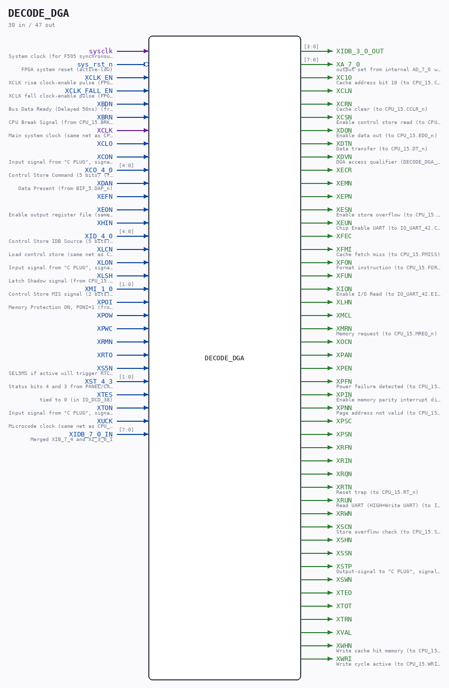
Schematic
Drawn from the Verilog: the yosys netlist of the Simulation (Verilator) build, instance CORE.CPU_BOARD.IO.DCD.DGA. Sub-modules are boxes (click the picture to open it full size; there every sub-module box links to its page, and every wire shows its Verilog name).
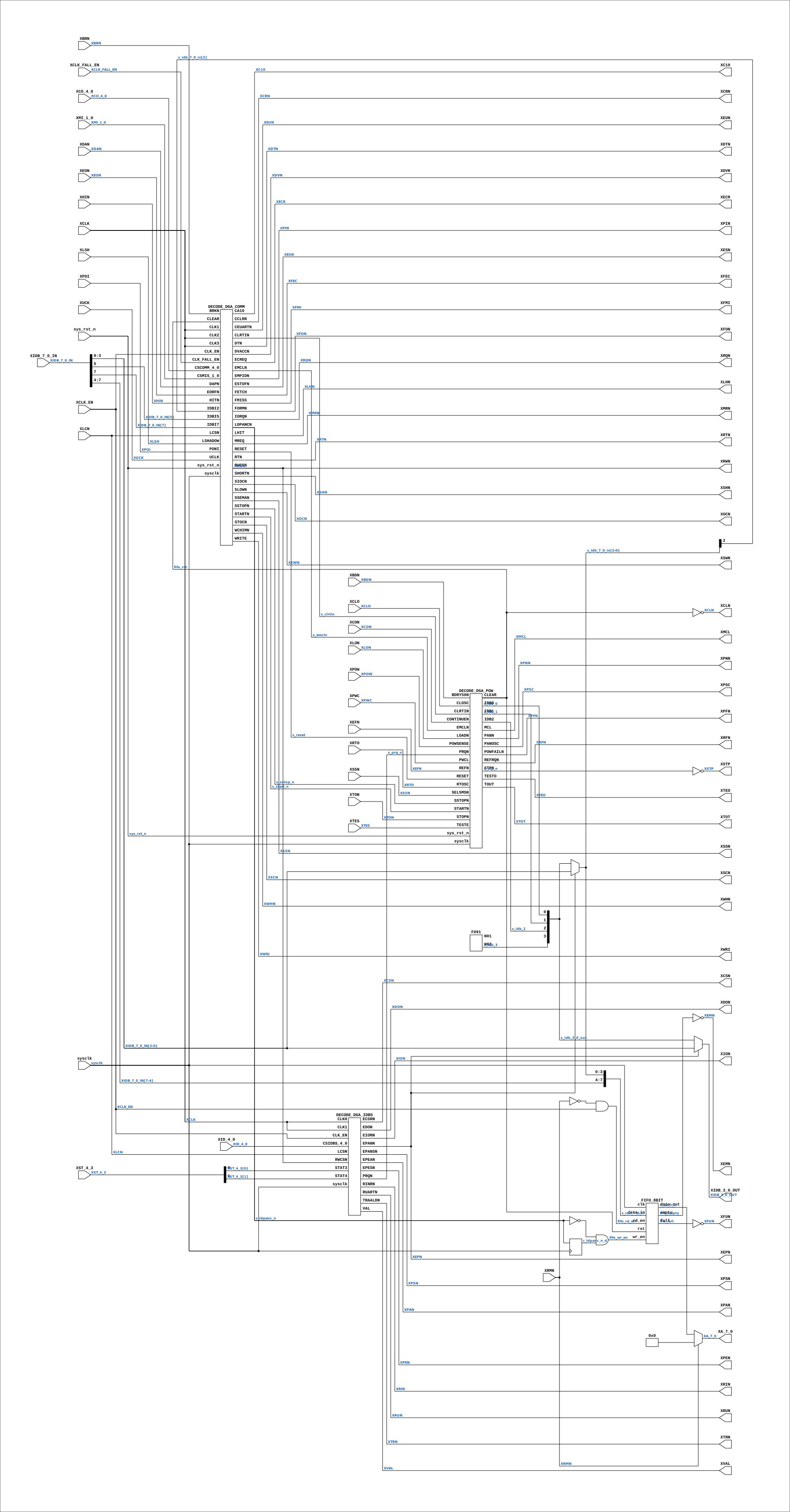
Description
ND120 DGA (Decode Gate Array) DECODE/DGA PDF Page 2 -> DECODE - DECODE_DGA- Sheet 1 of 6 PDF Page 3 -> DECODE - DECODE_DGA- Sheet 2 of 6 PDF Page 4 -> DECODE - DECODE_DGA- Sheet 3 of 6 PDF Page 5 -> DECODE - DECODE_DGA- Sheet 4 of 6 PDF Page 6 -> DECODE - DECODE_DGA- Sheet 5 of 6 PDF Page 7 -> DECODE - DECODE_DGA- Sheet 6 of 6 Last reviewed: 22-MAR-2025 Ronny Hansen
Ports
| Direction | Width | Name | Description |
|---|---|---|---|
| input | 1 |
sysclk |
System clock (for F595 synchronous RS latch) |
| input | 1 |
sys_rst_n (active low) |
FPGA system reset (active-low) |
| input | 1 |
XCLK_EN |
XCLK rise clock-enable pulse (FPGA_FF_MODE, else 0) |
| input | 1 |
XCLK_FALL_EN |
XCLK fall clock-enable pulse (FPGA_FF_MODE, else 0) |
| input | 1 |
XBDN |
Bus Data Ready (Delayed 50ns) (from BIF_5.BDRY50_n) |
| input | 1 |
XBRN |
CPU Break Signal (from CPU_15.BRK_n) |
| input | 1 |
XCLK |
Main system clock (same net as CPU_15.CLK) |
| input | 1 |
XCLO |
|
| input | 1 |
XCON |
Input signal from "C PLUG", signal B15 - CONTINUE_n (from ND3202D.CONTINUE_n) |
| input | [4:0] |
XCO_4_0 |
Control Store Command (5 bits) (from IO_37.CSCOMM_4_0) |
| input | 1 |
XDAN |
Data Present (from BIF_5.DAP_n) |
| input | 1 |
XEFN |
|
| input | 1 |
XEON |
Enable output register file (same net as CPU_15.EORF_n) |
| input | 1 |
XHIN |
|
| input | [4:0] |
XID_4_0 |
Control Store IDB Source (5 bits) (from IO_37.CSIDBS_4_0) |
| input | 1 |
XLCN |
Load control store (same net as CPU_15.LCS_n) |
| input | 1 |
XLON |
Input signal from "C PLUG", signal B12 - LOAD_n (from ND3202D.LOAD_n) |
| input | 1 |
XLSH |
Latch Shadow signal (from CPU_15.LSHADOW) |
| input | [1:0] |
XMI_1_0 |
Control Store MIS signal (2 bits) (from IO_37.CSMIS_1_0) |
| input | 1 |
XPOI |
Memory Protection ON, PONI=1 (from IO_DCD_38.PONI) |
| input | 1 |
XPOW |
|
| input | 1 |
XPWC |
|
| input | 1 |
XRMN |
|
| input | 1 |
XRTO |
|
| input | 1 |
XS5N |
SEL5MS if active will trigger RTC after 5 ms, not 20ms) (from ND3202D.SEL5MS_n) |
| input | [1:0] |
XST_4_3 |
Status bits 4 and 3 from PANEL/CALENDAR CPU 68705 (from IO_DCD_38.STAT_4_3) |
| input | 1 |
XTES |
tied to 0 (in IO_DCD_38) |
| input | 1 |
XTON |
Input signal from "C PLUG", signal B16 - STOP_n (from ND3202D.STOP_n) |
| input | 1 |
XUCK |
Microcode clock (same net as CPU_15.UCLK) |
| input | [7:0] |
XIDB_7_0_IN |
Merged XIB_7_4 and XI_3_0_I |
| output | [3:0] |
XIDB_3_0_OUT |
|
| output | [7:0] |
XA_7_0 |
output set from internal AD_7_0 when RMM_n is low(external signal XRMN) |
| output | 1 |
XC10 |
Cache address bit 10 (to CPU_15.CA10) |
| output | 1 |
XCLN |
|
| output | 1 |
XCRN |
Cache clear (to CPU_15.CCLR_n) |
| output | 1 |
XCSN |
Enable control store read (to CPU_15.ECSR_n) |
| output | 1 |
XDON |
Enable data out (to CPU_15.EDO_n) |
| output | 1 |
XDTN |
Data transfer (to CPU_15.DT_n) |
| output | 1 |
XDVN |
DGA access qualifier (DECODE_DGA_COMM A227, arrives as XDVN) - not the CGA's VACC (to IO_DCD_38.DVACC_n) |
| output | 1 |
XECR |
|
| output | 1 |
XEMN |
|
| output | 1 |
XEPN |
|
| output | 1 |
XESN |
Enable store overflow (to CPU_15.ESTOF_n) |
| output | 1 |
XEUN |
Chip Enable UART (to IO_UART_42.CEUART_n) |
| output | 1 |
XFEC |
|
| output | 1 |
XFMI |
Cache fetch miss (to CPU_15.FMISS) |
| output | 1 |
XFON |
Format instruction (to CPU_15.FORM_n) |
| output | 1 |
XFUN |
|
| output | 1 |
XION |
Enable I/O Read (to IO_UART_42.EIOR_n) |
| output | 1 |
XLHN |
|
| output | 1 |
XMCL |
|
| output | 1 |
XMRN |
Memory request (to CPU_15.MREQ_n) |
| output | 1 |
XOCN |
|
| output | 1 |
XPAN |
|
| output | 1 |
XPEN |
|
| output | 1 |
XPFN |
Power failure detected (to CPU_15.POWFAIL_n) |
| output | 1 |
XPIN |
Enable memory parity interrupt disable (to CPU_15.EMPID_n) |
| output | 1 |
XPNN |
Page address not valid (to CPU_15.PAN_n) |
| output | 1 |
XPSC |
|
| output | 1 |
XPSN |
|
| output | 1 |
XRFN |
|
| output | 1 |
XRIN |
|
| output | 1 |
XRQN |
|
| output | 1 |
XRTN |
Reset trap (to CPU_15.RT_n) |
| output | 1 |
XRUN |
Read UART (HIGH=Write UART) (to IO_UART_42.RUART_n) |
| output | 1 |
XRWN |
|
| output | 1 |
XSCN |
Store overflow check (to CPU_15.STOC_n) |
| output | 1 |
XSHN |
|
| output | 1 |
XSSN |
|
| output | 1 |
XSTP |
Output-signal to "C PLUG", signal B14 RUN~ (driven by Stop flip-flop: low while CPU is running) (to ND3202D.RUN_n) |
| output | 1 |
XSWN |
|
| output | 1 |
XTEO |
|
| output | 1 |
XTOT |
|
| output | 1 |
XTRN |
|
| output | 1 |
XVAL |
|
| output | 1 |
XWHN |
Write cache hit memory (to CPU_15.WCHIM_n) |
| output | 1 |
XWRI |
Write cycle active (to CPU_15.WRITE) |
Verilog source
Verilog/DECODE-GateArray/DGA/circuit/DECODE_DGA.v on GitHub.
Show the Verilog of DECODE_DGA (549 lines)
/**************************************************************************
** ND120 DGA (Decode Gate Array)                                         **
** DECODE/DGA                                                            **
**                                                                       **
** PDF Page 2 -> DECODE - DECODE_DGA- Sheet 1 of 6                       **
** PDF Page 3 -> DECODE - DECODE_DGA- Sheet 2 of 6                       **
** PDF Page 4 -> DECODE - DECODE_DGA- Sheet 3 of 6                       **
** PDF Page 5 -> DECODE - DECODE_DGA- Sheet 4 of 6                       **
** PDF Page 6 -> DECODE - DECODE_DGA- Sheet 5 of 6                       **
** PDF Page 7 -> DECODE - DECODE_DGA- Sheet 6 of 6                       **
**                                                                       **
** Last reviewed: 22-MAR-2025                                            **
** Ronny Hansen                                                          **
***************************************************************************/


module DECODE_DGA (
    input       sysclk,     // System clock (for F595 synchronous RS latch)
    input       sys_rst_n,  // FPGA system reset (active-low)
    input       XCLK_EN,      // XCLK rise clock-enable pulse (FPGA_FF_MODE, else 0)
    input       XCLK_FALL_EN, // XCLK fall clock-enable pulse (FPGA_FF_MODE, else 0)

    /*******************************************************************************
   ** The inputs are defined here                                                **
   *******************************************************************************/
    input       XBDN,         //! Bus Data Ready (Delayed 50ns) (from BIF_5.BDRY50_n)
    input       XBRN,         //! CPU Break Signal (from CPU_15.BRK_n)
    input       XCLK,         //! Main system clock (same net as CPU_15.CLK)
    input       XCLO,
    input       XCON,         //! Input signal from "C PLUG", signal B15 - CONTINUE_n (from ND3202D.CONTINUE_n)
    input [4:0] XCO_4_0,      //! Control Store Command (5 bits) (from IO_37.CSCOMM_4_0)
    input       XDAN,         //! Data Present (from BIF_5.DAP_n)
    input       XEFN,
    input       XEON,         //! Enable output register file (same net as CPU_15.EORF_n)
    input       XHIN,
    input [4:0] XID_4_0,      //! Control Store IDB Source (5 bits) (from IO_37.CSIDBS_4_0)

    input       XLCN,         //! Load control store (same net as CPU_15.LCS_n)
    input       XLON,         //! Input signal from "C PLUG", signal B12 - LOAD_n (from ND3202D.LOAD_n)
    input       XLSH,         //! Latch Shadow signal (from CPU_15.LSHADOW)
    input [1:0] XMI_1_0,      //! Control Store MIS signal (2 bits) (from IO_37.CSMIS_1_0)
    input       XPOI,         //! Memory Protection ON, PONI=1 (from IO_DCD_38.PONI)
    input       XPOW,
    input       XPWC,
    input       XRMN,
    input       XRTO,
    input       XS5N,         //! SEL5MS if active will trigger RTC after 5 ms, not 20ms) (from ND3202D.SEL5MS_n)
    input [1:0] XST_4_3,      //! Status bits 4 and 3 from PANEL/CALENDAR CPU 68705 (from IO_DCD_38.STAT_4_3)
    input       XTES,         //! tied to 0 (in IO_DCD_38)
    input       XTON,         //! Input signal from "C PLUG", signal B16 - STOP_n (from ND3202D.STOP_n)
    input       XUCK,         //! Microcode clock (same net as CPU_15.UCLK)


    input [7:0] XIDB_7_0_IN,  // Merged XIB_7_4 and XI_3_0_I

    // When reading this signal, check if XEPN (s_epan_n) = 0. If it is, then use these bits.

    // Its only the IDB[3:0] that is out (was named XIB_3_0_O).
    // With some control XI_3_0_C. XIDB[3] will always be zer0 when enabled out.
    // Output signal XEPN will also be low when XIDB_3_0_OUT is enabled out.
    output [3:0] XIDB_3_0_OUT,


    /*******************************************************************************
   ** The outputs are defined here                                               **
   *******************************************************************************/
    output [7:0] XA_7_0, // output set from internal AD_7_0 when RMM_n is low(external signal XRMN)
    //output [7:0] XA_7_0_C, // Not used (its a copy of the signal RMM_n but negated)
    output XC10,              //! Cache address bit 10 (to CPU_15.CA10)
    output XCLN,
    output XCRN,              //! Cache clear (to CPU_15.CCLR_n)
    output XCSN,              //! Enable control store read (to CPU_15.ECSR_n)
    output XDON,              //! Enable data out (to CPU_15.EDO_n)
    output XDTN,              //! Data transfer (to CPU_15.DT_n)
    output XDVN,              //! DGA access qualifier (DECODE_DGA_COMM A227, arrives as XDVN) - not the CGA's VACC (to IO_DCD_38.DVACC_n)
    output XECR,
    output XEMN,
    output XEPN,
    output XESN,              //! Enable store overflow (to CPU_15.ESTOF_n)
    output XEUN,              //! Chip Enable UART (to IO_UART_42.CEUART_n)
    output XFEC,
    output XFMI,              //! Cache fetch miss (to CPU_15.FMISS)
    output XFON,              //! Format instruction (to CPU_15.FORM_n)
    output XFUN,
    output XION,              //! Enable I/O Read (to IO_UART_42.EIOR_n)
    //output [3:0] XI_3_0_C,
    //output [3:0] XI_3_0_O,
    output XLHN,
    output XMCL,
    output XMRN,              //! Memory request (to CPU_15.MREQ_n)
    output XOCN,
    output XPAN,
    output XPEN,
    output XPFN,              //! Power failure detected (to CPU_15.POWFAIL_n)
    output XPIN,              //! Enable memory parity interrupt disable (to CPU_15.EMPID_n)
    output XPNN,              //! Page address not valid (to CPU_15.PAN_n)
    output XPSC,
    output XPSN,
    output XRFN,
    output XRIN,
    output XRQN,
    output XRTN,              //! Reset trap (to CPU_15.RT_n)
    output XRUN,              //! Read UART (HIGH=Write UART) (to IO_UART_42.RUART_n)
    output XRWN,
    output XSCN,              //! Store overflow check (to CPU_15.STOC_n)
    output XSHN,
    output XSSN,
    output XSTP,              //! Output-signal to "C PLUG", signal B14 RUN~ (driven by Stop flip-flop: low while CPU is running) (to ND3202D.RUN_n)
    output XSWN,
    output XTEO,
    output XTOT,
    output XTRN,
    output XVAL,
    output XWHN,              //! Write cache hit memory (to CPU_15.WCHIM_n)
    output XWRI               //! Write cycle active (to CPU_15.WRITE)
);

  /*******************************************************************************
   ** The wires are defined here                                                 **
   *******************************************************************************/
  wire [4:0] s_csidbs_4_0;
  wire [1:0] s_xmi_1_0;

  wire [3:0] s_idb_3_0_out;
  wire [1:0] s_xst_4_3;
  wire [7:0] s_idb_7_0_in;

  wire [7:0] s_ad_7_0;
  wire [4:0] s_cscomm_4_0;

  // Replaced by FIFO
  //wire [12:0] s_wel_12_0;
  //wire [12:0] s_weu_12_0;

  wire       s_xwhn;
  wire       s_ca10;
  wire       s_clrtin;
  wire       s_idb_2;
  wire       s_xteo;
  wire       s_idb_1;
  wire       s_xpsc;
  wire       s_xpoi;
  wire       s_xbrn;
  wire       s_xpan;
  wire       s_idb_3;
  wire       s_xpsn;
  wire       s_xshn;
  wire       s_xfmi;
  wire       s_xfon;
  wire       s_xlcn;
  wire       s_xs5n;
  wire       s_sstop_n;
  wire       s_stp_n;
  wire       s_xlon;
  wire       s_xton;
  wire       s_xfec;
  wire       s_xfun;
  wire       s_start_n;
  wire       s_prq_n;
  wire       s_reset;
  wire       s_xrqn;
  wire       s_xecr;
  wire       s_xdtn;
  wire       s_xeun;
  wire       s_xpnn;
  wire       s_xswn;
  wire       s_xrtn;
  wire       s_xlhn;
  wire       s_xtot;
  wire       s_xwri;
  wire       s_xocn;
  wire       s_xssn;
  wire       s_xbdn;
  wire       s_xlsh;
  wire       s_xrwn;
  wire       s_xrin;
  wire       s_xclk;
  wire       s_xion;
  wire       s_xdon;
  wire       s_xtrn;
  wire       s_xdan;
  wire       s_xhin;
  wire       s_xpwc;
  wire       s_xcsn;
  wire       s_xrun;
  wire       s_xpin;
  wire       s_uclk;
  wire       s_xesn;
  wire       s_xcrn;
  wire       s_xscn;
  wire       s_xrfn;
  wire       s_xtes;
  wire       s_ldpanc_n;
  wire       s_xeon;
  wire       s_xefn;
  wire       s_xpow;
  wire       s_xpfn;
  wire       s_idb_0;
  wire       s_xpen;
  wire       s_xmrn;
  wire       s_xval;
  wire       s_epan_n;
  wire       s_emcln;
  wire       s_xclo;
  wire       s_xcon;
  wire       s_xrm_n;
  wire       s_xrto;
  wire       s_xemn;
  wire       s_xcl_n;
  wire       s_xmcl;
  wire       s_xdvn;

  wire       s_clear;

  /*******************************************************************************
   ** Here all input connections are defined                                     **
   *******************************************************************************/

  // Bus connections
  assign s_csidbs_4_0[4:0] = XID_4_0;
  assign s_xmi_1_0[1:0]    = XMI_1_0;
  assign s_xst_4_3[1:0]    = XST_4_3;

  //assign s_idb_7_0_in[3:0]  = XI_3_0_I;
  //assign s_XIB_7_4[3:0] = XIB_7_4;

  // Signal s_idb_7_0_in goes as intput bus IDBI_7_0 to PFIFD
  // Normally all 8 bits are used, but when s_epan_n is low, only the high 4 bits from the external bus is used. Then the low bits come from the output from the DECODE_DGA_POW module.
  assign s_idb_7_0_in[7:4] = XIDB_7_0_IN[7:4];
  assign s_idb_7_0_in[3:0] = s_epan_n ? XIDB_7_0_IN[3:0] : {s_idb_3, s_idb_2, s_idb_1, s_idb_0};

  assign s_cscomm_4_0[4:0] = XCO_4_0;

  // Pin connections
  assign s_uclk            = XUCK;
  assign s_xbdn            = XBDN;
  assign s_xbrn            = XBRN;
  assign s_xclk            = XCLK;
  assign s_xclo            = XCLO;
  assign s_xcon            = XCON;
  assign s_xdan            = XDAN;
  assign s_xefn            = XEFN;
  assign s_xeon            = XEON;
  assign s_xhin            = XHIN;
  assign s_xlcn            = XLCN;
  assign s_xlon            = XLON;
  assign s_xlsh            = XLSH;
  assign s_xpoi            = XPOI;
  assign s_xpow            = XPOW;
  assign s_xpwc            = XPWC;
  assign s_xrm_n           = XRMN;
  assign s_xrto            = XRTO;
  assign s_xs5n            = XS5N;
  assign s_xtes            = XTES;
  assign s_xton            = XTON;

  /*******************************************************************************
   ** Here all output connections are defined                                    **
   *******************************************************************************/
  assign XA_7_0            = s_xrm_n ? 8'b0 : s_ad_7_0[7:0];
  // assign XI_3_0_C = s_XI_3_0_C[3:0]; Control signal not used
  //assign XI_3_0_O = s_idb_3_0_out[3:0];
  assign XIDB_3_0_OUT[3:0] = !s_epan_n ? s_idb_3_0_out[3:0] : XIDB_7_0_IN[3:0];

  assign XC10              = s_ca10;
  assign XCLN              = s_xcl_n;
  assign XCRN              = s_xcrn;
  assign XCSN              = s_xcsn;
  assign XDON              = s_xdon;
  assign XDTN              = s_xdtn;
  assign XDVN              = s_xdvn;
  assign XECR              = s_xecr;
  assign XEMN              = s_xemn;
  assign XEPN              = s_epan_n;
  assign XESN              = s_xesn;
  assign XEUN              = s_xeun;
  assign XFEC              = s_xfec;
  assign XFMI              = s_xfmi;
  assign XFON              = s_xfon;
  assign XFUN              = s_xfun;
  assign XION              = s_xion;
  assign XLHN              = s_xlhn;
  assign XMCL              = s_xmcl;
  assign XMRN              = s_xmrn;
  assign XOCN              = s_xocn;
  assign XPAN              = s_xpan;
  assign XPEN              = s_xpen;
  assign XPFN              = s_xpfn;
  assign XPIN              = s_xpin;
  assign XPNN              = s_xpnn;
  assign XPSC              = s_xpsc;
  assign XPSN              = s_xpsn;
  assign XRFN              = s_xrfn;
  assign XRIN              = s_xrin;
  assign XRQN              = s_xrqn;
  assign XRTN              = s_xrtn;
  assign XRUN              = s_xrun;
  assign XRWN              = s_xrwn;
  assign XSCN              = s_xscn;
  assign XSHN              = s_xshn;
  assign XSSN              = s_xssn;
  assign XSTP              = ~s_stp_n;
  assign XSWN              = s_xswn;
  assign XTEO              = s_xteo;
  assign XTOT              = s_xtot;
  assign XTRN              = s_xtrn;
  assign XVAL              = s_xval;
  assign XWHN              = s_xwhn;
  assign XWRI              = s_xwri;


  /*******************************************************************************
   ** Here all normal components are defined                                     **
   *******************************************************************************/

  assign s_idb_3_0_out     = {s_idb_3, s_idb_2, s_idb_1, s_idb_0};
  assign s_xcl_n           = ~s_clear;


  /*******************************************************************************
   ** Here all sub-circuits are defined                                          **
   *******************************************************************************/

  /* verilator lint_off PINCONNECTEMPTY */
  F091 A090 (
      .N01(),
      .N02(s_idb_3)
  );
  /* verilator lint_on PINCONNECTEMPTY */

  /*
   DECODE_DGA_PFIFC   PFIFC (.CLEAR(s_xcln),
                             .EMPN(s_xemn),
                             .FULN(s_xfun),
                             .LDPANCN(s_ldpanc_n),
                             .RMMN(s_xrm_n),
                             .WEL_12_0(s_wel_12_0[12:0]),
                             .WEU_12_0(s_weu_12_0[12:0]));


   DECODE_DGA_PFIFD   PFIFD (.AD_7_0(s_ad_7_0[7:0]),
         .IDBI_7_0(s_idb_7_0_in[7:0]),
         .WEL_12_0(s_wel_12_0[12:0]),
         .WEU_12_0(s_weu_12_0[12:0]));


   */

  // ***********************************************************************************************************
  // * Instantiate the FIFO module that replace DECODE_DGA_PFIFD, DECODE_DGA_PFIFC and DECODE_DGA_PFIFC_DELAY  *
  // ***********************************************************************************************************

  // FIFO IN wires
  wire fifo_rst = ~s_xcl_n;
  // The original PFIFC/PFIFD wrote a byte on the LDPANC~ pulse itself.
  // LDPANC~ = ~(EROF & ldpanc_latched) (DECODE_DGA_COMM A195): EROF is the
  // CYC/PAL_44307C "misc write pulse" of cycle state d, ONE sysclk wide,
  // mid-cycle - it never coincides with an XCLK rise. Gating the write with
  // XCLK_EN (FF mode) or clocking it on XCLK (latch mode) therefore NEVER
  // wrote a byte: the CPU->panel direction was dead since the FIFO replaced
  // the PFIF* blocks (measured 28-AUG-2026, sim/examples/panel_pans_capture.py
  // with PANS_TRIG="CSA_12_0 == o1045": ldpanc_n low for 1 sysclk, XCLK_EN=0,
  // wr_ptr stayed 0). The FIFO now clocks on sysclk in both modes; the write
  // is the sysclk-detected FALLING edge of LDPANC~ (one byte per pulse), the
  // pop is one per XCLK rise while RMM~ is low (XCLK_EN in FF mode, the
  // detected XCLK rise in latch mode) - the DGA pops one byte per XCLK
  // while the 68705 holds RMM~ low, as before.
  reg r_ldpanc_n_d = 1'b1;
  reg r_xclk_d     = 1'b0;
  always @(posedge sysclk) begin
    r_ldpanc_n_d <= s_ldpanc_n;
    r_xclk_d     <= s_xclk;
  end
  wire fifo_clk   = sysclk;
  wire fifo_wr_en = ~s_ldpanc_n & r_ldpanc_n_d;   // LDPANC~ falling edge
`ifdef FPGA_FF_MODE
  wire fifo_rd_en = ~s_xrm_n & XCLK_EN;
`else
  wire fifo_rd_en = ~s_xrm_n & s_xclk & ~r_xclk_d;  // XCLK rising edge
`endif

  // FIFO OUT wires
  wire fifo_full;
  wire fifo_empty;

  assign s_xfun = ~fifo_full;
  assign s_xemn = ~fifo_empty;

  //assign fifo_full= 0; // assign during debug

  FIFO_8BIT #(
      .DEPTH(13)  // Depth of the FIFO (maximum 16)
  ) fifo_inst (
      .clk(fifo_clk),
      .rst(fifo_rst),
      .wr_en(fifo_wr_en),
      .rd_en(fifo_rd_en),
      .data_in(s_idb_7_0_in),
      // out
      .data_out(s_ad_7_0),
      .full(fifo_full),
      .empty(fifo_empty)
  );

`ifdef ND120_PANEL_CLOCK_TRACE
  // Sim-only: every byte pushed into the panel FIFO (LDPANC) and every
  // MAPANS (TRA PANS) so the CPU side of the panel protocol is visible.
  always @(posedge fifo_clk) begin
    if (fifo_wr_en && !fifo_full) $display("[dga] t=%0t LDPANC push %03o", $time, s_idb_7_0_in);
    if (fifo_wr_en &&  fifo_full) $display("[dga] t=%0t LDPANC push %03o DROPPED (FIFO full)", $time, s_idb_7_0_in);
  end
  reg r_trc_mapans = 1'b0;
  always @(posedge sysclk) begin
    r_trc_mapans <= IDBS.s_mapans;
    if (IDBS.s_mapans && !r_trc_mapans) $display("[dga] t=%0t MAPANS (TRA PANS)", $time);
  end
`endif

  // ****************************************************************************************************
  // FIFO MODULE END
  // ****************************************************************************************************

  DECODE_DGA_POW POW (
      .sysclk(sysclk),
      .sys_rst_n(sys_rst_n),
      // Inputs
      .BDRY50N(s_xbdn),
      .CLOSC(s_xclo),
      .CLRTIN(s_clrtin),
      .CONTINUEN(s_xcon),
      .EMCLN(s_emcln),
      .LOADN(s_xlon),
      .POWSENSE(s_xpow),
      .PRQN(s_prq_n),
      .PWCL(s_xpwc),
      .REFN(s_xefn),
      .RESET(s_reset),
      .RTOSC(s_xrto),
      .SEL5MSN(s_xs5n),
      .SSTOPN(s_sstop_n),
      .STARTN(s_start_n),
      .STOPN(s_xton),
      .TESTE(s_xtes),

      // Outputs
      .CLEAR(s_clear),
      .IDB0(s_idb_0),
      .IDB1(s_idb_1),
      .IDB2(s_idb_2),
      .MCL(s_xmcl),
      .PANN(s_xpnn),
      .PANOSC(s_xpsc),
      .POWFAILN(s_xpfn),
      .REFRQN(s_xrfn),
      .STPN(s_stp_n),
      .TESTO(s_xteo),
      .TOUT(s_xtot)
  );


  // Decode SOURCE signal for IDB bus
  DECODE_DGA_IDBS IDBS (
    // P2 clock-enable (FPGA_FF_MODE)
    .sysclk(sysclk),
    .CLK_EN(XCLK_EN),
    // Clock inputs
    .CLK0(s_xclk),           // Clock input 0
    .CLK1(s_xclk),           // Clock input 1

    // Control/Status inputs
    .CSIDBS_4_0(s_csidbs_4_0[4:0]),  // 5-bit control input
    .LCSN(s_xlcn),
    .RWCSN(s_xrwn),          // the DGA's OWN RWCS decode (COMM sheet output, net s_xrwn) - gates the IDBS sheet's simulation-compensation window
    .STAT3(s_xst_4_3[0]),    // Status bit 4 from PANEL/CALENDAR CPU 68705
    .STAT4(s_xst_4_3[1]),    // Status bit 4 from PANEL/CALENDAR CPU 68705

    // Status/Control outputs
    .ECSRN(s_xcsn),          // Enable Cache Status Register (CSR) - 24
    .EDON(s_xdon),           // Enable DO signal (multiple IDB sources) - 0,1,2,3,4,6,10,11,14,25,36
    .EIORN(s_xion),          // Enable IO register from UART etc -16
    .EPANN(s_epan_n),        // Enable Panel Interrupt Vector - 27
    .EPANSN(s_xpsn),         // Enable Panel Status register (MIPANS/MAPANS - 20/21
    .EPEAN(s_xpan),          // Enable Parity Error address (PEA) - 12
    .EPESN(s_xpen),          // Enable Parity Error Status & Address (PES) -13
    .RINRN(s_xrin),          // Read Installation Number (RINR) - 35
    .RUARTN(s_xrun),         // Read UART - 37
    .TRAALDN(s_xtrn),        // Read Automatic Load Descriptor and print-status (ALD) - 26 ('TRA ALD' opcode)

    .PRQN(s_prq_n),          // Panel Request (Read MIPANS)
    .VAL(s_xval)             // Panel Interrupt (Panel Status Register bit 12 on read)
);

  DECODE_DGA_COMM COMM (
      .sysclk(sysclk),
      .sys_rst_n(sys_rst_n),
      .CLK_EN(XCLK_EN),           //! P2 clock-enable (CLK rise, FPGA_FF_MODE)
      .CLK_FALL_EN(XCLK_FALL_EN), //! P2 clock-enable (CLK fall, FPGA_FF_MODE)
      // Inputs
      .BRKN(s_xbrn),         //! Break signal
      .CA10(s_ca10),         //! Cache address bit 10
      .CLEAR(s_clear),       //! Clear signal
      .CLK1(s_xclk),         //! Clock input 1
      .CLK2(s_xclk),         //! Clock input 2
      .CLK3(s_xclk),         //! Clock input 3
      .CLRTIN(s_clrtin),     //! Clear Real Time Clock
      .CSCOMM_4_0(s_cscomm_4_0[4:0]), //! Microcode Command 4:0
      .CSMIS_1_0(s_xmi_1_0[1:0]),     //! Microcode Misc signal 1:0
      .EMCLN(s_emcln),       //! Enable Master Clear
      .FETCH(s_xfec),        //! Fetch cycle active
      .FMISS(s_xfmi),        //! Cache miss during fetch
      .IDBI2(s_idb_7_0_in[2]), //! Internal data bus input bit 2
      .IDBI5(s_idb_7_0_in[5]), //! Internal data bus input bit 5
      .IDBI7(s_idb_7_0_in[7]), //! Internal data bus input bit 7
      .LCSN(s_xlcn),         //! Load Control Store
      .LHIT(s_xlhn),         //! Cache hit during load
      .LSHADOW(s_xlsh),      //! Load shadow
      .PONI(s_xpoi),         //! Memory Protection ON, PONI=1
      .RESET(s_reset),       //! Reset signal
      .SSTOPN(s_sstop_n),    //! Set Stop Flip-Flop
      .STARTN(s_start_n),    //! Start signal
      .UCLK(s_uclk),         //! U clock
      .WRITE(s_xwri),        //! Write cycle active
      .EORFN(s_xeon),        //! Enable Output Register

      // Outputs
      .CCLRN(s_xcrn),
      .CEUARTN(s_xeun),
      .DAPN(s_xdan),
      .DTN(s_xdtn),
      .DVACCN(s_xdvn),
      .ECREQ(s_xecr),
      .EMPIDN(s_xpin),        //! CSCOMM=12, SMPID -  Set bits in the micro—P10 (Priority Interrupt Detect) register in the PIC.
      .ESTOFN(s_xesn),
      .FORMN(s_xfon),
      .HITN(s_xhin),
      .IORQN(s_xrqn),
      .LDPANCN(s_ldpanc_n),
      .MREQ(s_xmrn),
      .RTN(s_xrtn),
      .RWCSN(s_xrwn),
      .SHORTN(s_xshn),
      .SIOCN(s_xocn),
      .SLOWN(s_xswn),
      .SSEMAN(s_xssn),
      .STOCN(s_xscn),
      .WCHIMN(s_xwhn)
  );

endmodule