DECODE_DGA_IDBS
Source: Verilog/DECODE-GateArray/DGA/circuit/DECODE_DGA_IDBS.v
Where it sits (Simulation): ND120_TOP > ND120_CORE > ND3202D > IO_37 > IO_DCD_38 > DECODE_DGA > DECODE_DGA_IDBS
- instance path: CORE.CPU_BOARD.IO.DCD.DGA.IDBS
Used in: DECODE_DGA (all tops)
Module hierarchy - All modules
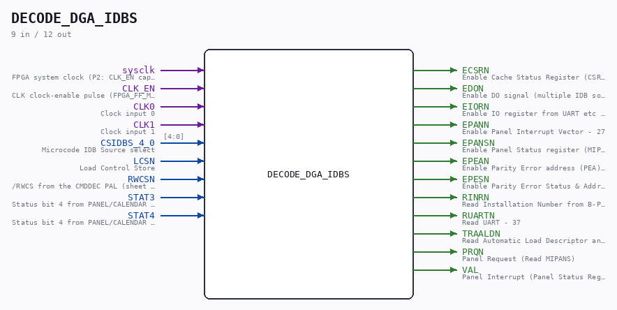
Schematic
Drawn from the Verilog: the yosys netlist of the Simulation (Verilator) build, instance CORE.CPU_BOARD.IO.DCD.DGA.IDBS. Sub-modules are boxes (click the picture to open it full size; there every sub-module box links to its page, and every wire shows its Verilog name).
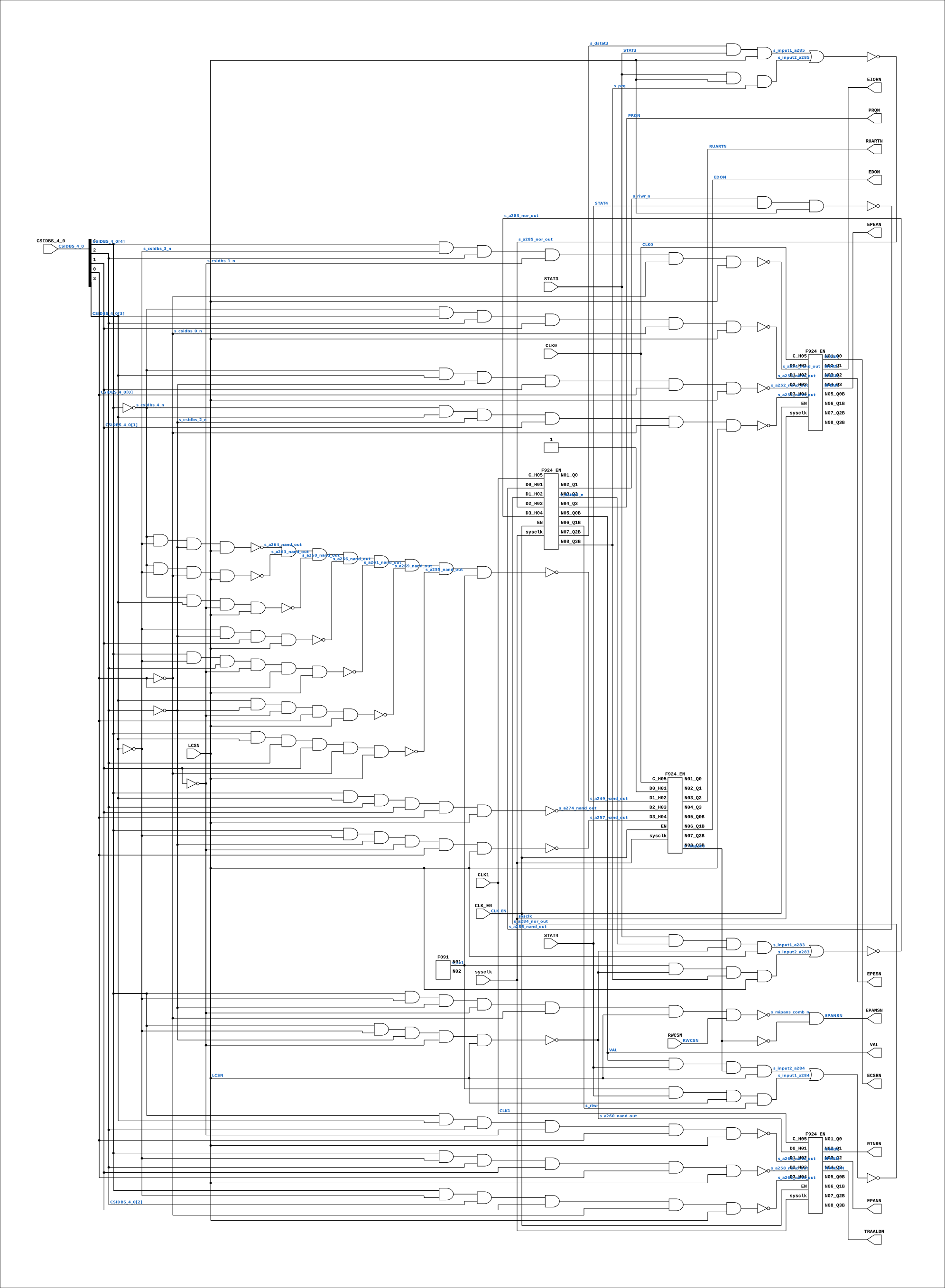
Description
ND120 DGA (Decode Gate Array) DECODE/DGA/IDBS Decode Internal Databus SOURCE (IDBS). Generates ENABLE signals for the chips to be read or written Page 14 DECODE - DECODE_DGA_IDBS Sheet 1 of 2 Page 15 DECODE - DECODE_DGA_IDBS Sheet 2 of 2 Last reviewed: 2-FEB-2025 Ronny Hansen
Ports
| Direction | Width | Name | Description |
|---|---|---|---|
| input | 1 |
sysclk |
FPGA system clock (P2: CLK_EN capture) |
| input | 1 |
CLK_EN |
CLK clock-enable pulse (FPGA_FF_MODE, else 0) |
| input | 1 |
CLK0 |
Clock input 0 |
| input | 1 |
CLK1 |
Clock input 1 |
| input | [4:0] |
CSIDBS_4_0 |
Microcode IDB Source select |
| input | 1 |
LCSN |
Load Control Store |
| input | 1 |
RWCSN |
/RWCS from the CMDDEC PAL (sheet 34). NOT a gate-array pin - a |
| input | 1 |
STAT3 |
Status bit 4 from PANEL/CALENDAR CPU 68705 |
| input | 1 |
STAT4 |
Status bit 4 from PANEL/CALENDAR CPU 68705 |
| output | 1 |
ECSRN |
Enable Cache Status Register (CSR) - 24 |
| output | 1 |
EDON |
Enable DO signal (multiple IDB sources) - 0,1,2,3,4,6,10,11,14,25,36 |
| output | 1 |
EIORN |
Enable IO register from UART etc -16 |
| output | 1 |
EPANN |
Enable Panel Interrupt Vector - 27 |
| output | 1 |
EPANSN |
Enable Panel Status register (MIPANS/MAPANS - 20/21 |
| output | 1 |
EPEAN |
Enable Parity Error address (PEA) - 12 |
| output | 1 |
EPESN |
Enable Parity Error Status & Address (PES) -13 |
| output | 1 |
RINRN |
Read Installation Number from B-PLUG (RINR) - IDBS=35 |
| output | 1 |
RUARTN |
Read UART - 37 |
| output | 1 |
TRAALDN |
Read Automatic Load Descriptor and print-status (ALD) - 26 |
| output | 1 |
PRQN |
Panel Request (Read MIPANS) |
| output | 1 |
VAL |
Panel Interrupt (Panel Status Register bit 12 on read) |
Verilog source
Verilog/DECODE-GateArray/DGA/circuit/DECODE_DGA_IDBS.v on GitHub.
Show the Verilog of DECODE_DGA_IDBS (662 lines)
/**************************************************************************
** ND120 DGA (Decode Gate Array)                                         **
** DECODE/DGA/IDBS                                                       **
**                                                                       **
** Decode Internal Databus SOURCE (IDBS). Generates ENABLE signals for   **
** the chips to be read or written                                       **
**                                                                       **
** Page 14 DECODE - DECODE_DGA_IDBS Sheet 1 of 2                         **
** Page 15 DECODE - DECODE_DGA_IDBS Sheet 2 of 2                         **
**                                                                       **
** Last reviewed: 2-FEB-2025                                             **
** Ronny Hansen                                                          **
***************************************************************************/

module DECODE_DGA_IDBS (
    input       sysclk,      //! FPGA system clock (P2: CLK_EN capture)
    input       CLK_EN,      //! CLK clock-enable pulse (FPGA_FF_MODE, else 0)
    input       CLK0,        //! Clock input 0
    input       CLK1,        //! Clock input 1
    input [4:0] CSIDBS_4_0,  //! Microcode IDB Source select
    input       LCSN,        //! Load Control Store
    input       RWCSN,       //! /RWCS from the CMDDEC PAL (sheet 34). NOT a gate-array pin - a
                             //! simulation-compensation input, see the EPANSN note below. Tie
                             //! high to get the pin-exact gate array.
    input       STAT3,       //! Status bit 4 from PANEL/CALENDAR CPU 68705
    input       STAT4,       //! Status bit 4 from PANEL/CALENDAR CPU 68705

    output ECSRN,   //! Enable Cache Status Register (CSR) - 24
    output EDON,    //! Enable DO signal (multiple IDB sources) - 0,1,2,3,4,6,10,11,14,25,36
    output EIORN,   //! Enable IO register from UART etc -16
    output EPANN,   //! Enable Panel Interrupt Vector - 27
    output EPANSN,  //! Enable Panel Status register (MIPANS/MAPANS - 20/21
    output EPEAN,   //! Enable Parity Error address (PEA) - 12
    output EPESN,   //! Enable Parity Error Status & Address (PES) -13
    output RINRN,   //! Read Installation Number from B-PLUG (RINR) - IDBS=35
    output RUARTN,  //! Read UART - 37
    output TRAALDN, //! Read Automatic Load Descriptor and print-status (ALD) - 26

    output PRQN,  //! Panel Request (Read MIPANS)
    output VAL    //! Panel Interrupt (Panel Status Register bit 12 on read)
);
  /*******************************************************************************
   ** The wires are defined here                                                 **
   *******************************************************************************/
  wire [4:0] s_csidbs_4_0;
  wire       s_a250_nand_out;
  wire       s_rinr_n;
  wire       s_val;
  wire       s_a253_nand_out;
  wire       s_a261_nand_out;
  wire       s_a265_nand_out;
  wire       s_a274_nand_out;
  wire       s_input2_a285;
  wire       s_a255_nand_out;
  wire       s_input2_a284;
  wire       s_input1_a283;
  wire       s_input1_a285;
  wire       s_riwr_n;
  wire       s_a283_nor_out;
  wire       s_edo_n;
  wire       s_a286_nand_out;
  wire       s_traald_n;
  wire       s_dstat3_n;
  wire       s_a258_nand_out;
  wire       s_riwr;
  wire       s_a256_nand_out;
  wire       s_a263_nand_out;
  wire       s_clk1;
  wire       s_a257_nand_out;
  wire       s_a251_nand_out;
  wire       s_prq;
  wire       s_ruart_n;
  wire       s_csidbs_0_n;
  wire       s_a260_nand_out;

  wire       s_input2_a283;

  wire       s_csidbs_4_n;
  wire       s_clk0;
  wire       s_stat_4;
  wire       s_input1_a284;
  wire       s_epans_n;
  wire       s_epans_reg_n;   //! A259 Q0 - the REGISTERED MIPANS/MAPANS decode, as the real DGA has it
  wire       s_rwcs_n;        //! see RWCSN
  wire       s_a284_nor_out;

  wire       s_a262_nand_out;
  wire       s_eior_n;
  wire       s_ecsr_n;
  wire       s_vcc;
  wire       s_csidbs_1_n;
  wire       s_dstat3;
  wire       s_a254_nand_out;


  wire       s_mapans;
  wire       s_lcs_n;
  wire       s_epan_n;
  wire       s_epea_n;
  wire       s_prq_n;
  wire       s_epes_n;
  wire       s_csidbs_2_n;
  wire       s_a269_nand_out;
  wire       s_zz1;
  wire       s_csidbs_3_n;
  wire       s_a252_nand_out;
  wire       s_a285_nor_out;
  wire       s_stat_3;
  wire       s_a249_nand_out;
  wire       s_a264_nand_out;

  /*******************************************************************************
   ** The module functionality is described here                                 **
   *******************************************************************************/

  /*******************************************************************************
   ** Here all input connections are defined                                     **
   *******************************************************************************/
  assign s_csidbs_4_0[4:0] = CSIDBS_4_0;
  assign s_rwcs_n          = RWCSN;
  assign s_clk1 = CLK1;
  assign s_clk0 = CLK0;

  // P2 (docs/plan-fix-unconstrained-clocks.md): in FF mode the CLK-clocked
  // registers (CLK0 and CLK1 are both the board CLK, XCLK) capture on
  // posedge sysclk gated by CLK_EN (aligned to the CLK rise) instead of
  // clocking on the routed net.
`ifdef FPGA_FF_MODE
  localparam CLK_CE = 1;
`else
  localparam CLK_CE = 0;
`endif
  assign s_stat_4 = STAT4;
  assign s_lcs_n = LCSN;
  assign s_stat_3 = STAT3;

  /*******************************************************************************
   ** Here all output connections are defined                                    **
   *******************************************************************************/
  assign ECSRN = s_ecsr_n;
  assign EDON = s_edo_n;
  assign EIORN = s_eior_n;
  assign EPANN = s_epan_n;
  assign EPANSN = s_epans_n;
  assign EPEAN = s_epea_n;
  assign EPESN = s_epes_n;
  assign PRQN = s_prq_n;
  assign RINRN = s_rinr_n;
  assign RUARTN = s_ruart_n;
  assign TRAALDN = s_traald_n;
  assign VAL = s_val;

  /*******************************************************************************
   ** Here all in-lined components are defined                                   **
   *******************************************************************************/

  // Power
  assign s_vcc = 1'b1;


  // NOT Gate
  assign s_csidbs_0_n = ~s_csidbs_4_0[0];

  // NOT Gate
  assign s_csidbs_1_n = ~s_csidbs_4_0[1];

  // NOT Gate
  assign s_csidbs_2_n = ~s_csidbs_4_0[2];

  // NOT Gate
  assign s_csidbs_3_n = ~s_csidbs_4_0[3];

  // NOT Gate
  assign s_csidbs_4_n = ~s_csidbs_4_0[4];

  /*******************************************************************************
   ** Here all normal components are defined                                     **
   *******************************************************************************/
  /*
   NOR_GATE #(.BubblesMask(2'b00))
      A284 (.input1(s_input2_a284),
            .input2(s_input1_a284),
            .result(s_a284_nor_out));
   */

  // A284 NOR_GATE
  assign s_a284_nor_out = ~(s_input2_a284 | s_input1_a284);

  /*
   NOR_GATE #(.BubblesMask(2'b00))
      A285 (.input1(s_input1_a285),
            .input2(s_input2_a285),
            .result(s_a285_nor_out));
   */
  // A285 NOR_GATE
  assign s_a285_nor_out = ~(s_input1_a285 | s_input2_a285);

  /*
   NOR_GATE #(.BubblesMask(2'b00))
      A283 (.input1(s_input1_a283),
            .input2(s_input2_a283),
            .result(s_a283_nor_out));
   */
  // A283 NOR_GATE
  assign s_a283_nor_out = ~(s_input1_a283 | s_input2_a283);

  /*
   NAND_GATE_3_INPUTS #(.BubblesMask(3'b000))
      A286 (.input1(s_riwr_n),
            .input2(s_stat_4),
            .input3(s_lcs_n),
            .result(s_a286_nand_out));
   */
  // A286 NAND_GATE_3_INPUTS
  assign s_a286_nand_out = ~(s_riwr_n & s_stat_4 & s_lcs_n);

  /*
   NAND_GATE_4_INPUTS #(.BubblesMask(4'h0))
      A264 (.input1(s_csidbs_4_n),
            .input2(s_csidbs_3_n),
            .input3(s_csidbs_2_n),
            .input4(s_lcs_n),
            .result(s_a264_nand_out));
   */
  //A264 NAND_GATE_4_INPUTS
  assign s_a264_nand_out = ~(s_csidbs_4_n & s_csidbs_3_n & s_csidbs_2_n & s_lcs_n);

  /*
   NAND_GATE_6_INPUTS #(.BubblesMask({2'b00, 4'h0}))
      A262 (.input1(s_csidbs_4_0[4]),
            .input2(s_csidbs_3_n),
            .input3(s_csidbs_4_0[2]),
            .input4(s_csidbs_4_0[1]),
            .input5(s_csidbs_0_n),
            .input6(s_lcs_n),
            .result(s_a262_nand_out));
   */
  // A262 NAND_GATE_6_INPUTS
  assign s_a262_nand_out = ~(s_csidbs_4_0[4] & s_csidbs_3_n & s_csidbs_4_0[2] & s_csidbs_4_0[1] & s_csidbs_0_n & s_lcs_n);

  /*
   NAND_GATE_4_INPUTS #(.BubblesMask(4'h0))
      A263 (.input1(s_csidbs_4_n),
            .input2(s_csidbs_3_n),
            .input3(s_csidbs_0_n),
            .input4(s_lcs_n),
            .result(s_a263_nand_out));
   */
  // A263 NAND_GATE_4_INPUTS
  assign s_a263_nand_out = ~(s_csidbs_4_n & s_csidbs_3_n & s_csidbs_0_n & s_lcs_n);

  /*
   NAND_GATE_6_INPUTS #(.BubblesMask({2'b00, 4'h0}))
      A258 (.input1(s_csidbs_4_0[4]),
            .input2(s_csidbs_3_n),
            .input3(s_csidbs_4_0[2]),
            .input4(s_csidbs_4_0[1]),
            .input5(s_csidbs_4_0[0]),
            .input6(s_lcs_n),
            .result(s_a258_nand_out));
   */
  // A258 NAND_GATE_6_INPUTS
  assign s_a258_nand_out = ~(s_csidbs_4_0[4] & s_csidbs_3_n & s_csidbs_4_0[2] & s_csidbs_4_0[1] & s_csidbs_4_0[0] & s_lcs_n);

  /*
   NAND_GATE_4_INPUTS #(.BubblesMask(4'h0))
      A250 (.input1(s_csidbs_4_n),
            .input2(s_csidbs_4_0[3]),
            .input3(s_csidbs_1_n),
            .input4(s_lcs_n),
            .result(s_a250_nand_out));
   */
  //A250 NAND_GATE_4_INPUTS = 01n1n = 12=PEA,13=PES,16=IOR,17=NONE
  assign s_a250_nand_out = ~(s_csidbs_4_n & s_csidbs_4_0[3] & s_csidbs_1_n & s_lcs_n);

  /*
   NAND_GATE_4_INPUTS #(.BubblesMask(4'h0))
      A256 (.input1(s_csidbs_3_n),
            .input2(s_csidbs_2_n),
            .input3(s_csidbs_4_0[1]),
            .input4(s_lcs_n),
            .result(s_a256_nand_out));
   */

  //A256 NAND_GATE_4_INPUTS = n001n, 2=GPR,3=DBR,22=GPR_SE,23=PGS
  assign s_a256_nand_out = ~(s_csidbs_3_n & s_csidbs_2_n & s_csidbs_4_0[1] & s_lcs_n);

  /*
   NAND_GATE_8_INPUTS #(.BubblesMask(8'h00))
      A249 (.input1(s_a264_nand_out),
            .input2(s_a263_nand_out),
            .input3(s_a250_nand_out),
            .input4(s_a256_nand_out),
            .input5(s_a261_nand_out),
            .input6(s_a269_nand_out), //269
            .input7(s_a255_nand_out),
            .input8(s_zz1),
            .result(s_a249_nand_out));
   */

  // A249 NAND_GATE_8_INPUTS
  assign s_a249_nand_out = ~(s_a264_nand_out & s_a263_nand_out & s_a250_nand_out & s_a256_nand_out & s_a261_nand_out & s_a269_nand_out & s_a255_nand_out & s_zz1);

  /*
   NAND_GATE_6_INPUTS #(.BubblesMask({2'b00, 4'h0}))
      A265 (.input1(s_csidbs_4_0[4]),
            .input2(s_csidbs_4_0[3]),
            .input3(s_csidbs_4_0[2]),
            .input4(s_csidbs_1_n),
            .input5(s_csidbs_4_0[0]),
            .input6(s_lcs_n),
            .result(s_a265_nand_out));
   */
  // A265 NAND_GATE_6_INPUTS
  assign s_a265_nand_out = ~(s_csidbs_4_0[4] & s_csidbs_4_0[3] & s_csidbs_4_0[2] & s_csidbs_1_n & s_csidbs_4_0[0] & s_lcs_n);

  /*
   NAND_GATE_6_INPUTS #(.BubblesMask({2'b00, 4'h0}))
      A261 (.input1(s_csidbs_4_0[4]),
            .input2(s_csidbs_3_n),
            .input3(s_csidbs_4_0[2]),
            .input4(s_csidbs_1_n),
            .input5(s_csidbs_4_0[0]),
            .input6(s_lcs_n),
            .result(s_a261_nand_out));
   */
  // A261 NAND_GATE_6_INPUTS
  assign s_a261_nand_out = ~(s_csidbs_4_0[4] & s_csidbs_3_n & s_csidbs_4_0[2] & s_csidbs_1_n & s_csidbs_4_0[0] & s_lcs_n);

  /*
   NAND_GATE_5_INPUTS #(.BubblesMask({1'b0, 4'h0}))
      A260 (.input1(s_csidbs_4_0[4]),
            .input2(s_csidbs_3_n),
            .input3(s_csidbs_2_n),
            .input4(s_csidbs_1_n),
            .input5(s_lcs_n),
            .result(s_a260_nand_out));
   */
  // A260 NAND_GATE_5_INPUTS
  assign s_a260_nand_out = ~(s_csidbs_4_0[4] & s_csidbs_3_n & s_csidbs_2_n & s_csidbs_1_n & s_lcs_n);

  /*
   NAND_GATE_5_INPUTS #(.BubblesMask({1'b0, 4'h0}))
      A269 (.input1(s_csidbs_4_0[3]),
            .input2(s_csidbs_2_n),
            .input3(s_csidbs_1_n),
            .input4(s_csidbs_4_0[0]),
            .input5(s_lcs_n),
            .result(s_a269_nand_out));
   */
  // A269 NAND_GATE_5_INPUTS
  assign s_a269_nand_out = ~(s_csidbs_4_0[3] & s_csidbs_2_n & s_csidbs_1_n & s_csidbs_4_0[0] & s_lcs_n);

  /*
   NAND_GATE_6_INPUTS #(.BubblesMask({2'b00, 4'h0}))
      A255 (.input1(s_csidbs_4_0[4]),
            .input2(s_csidbs_4_0[3]),
            .input3(s_csidbs_4_0[2]),
            .input4(s_csidbs_4_0[1]),
            .input5(s_csidbs_0_n),
            .input6(s_lcs_n),
            .result(s_a255_nand_out));
   */
  //A255 NAND_GATE_6_INPUTS
  assign s_a255_nand_out = ~(s_csidbs_4_0[4] & s_csidbs_4_0[3] & s_csidbs_4_0[2] & s_csidbs_4_0[1] & s_csidbs_0_n & s_lcs_n);

  /*
   NAND_GATE_6_INPUTS #(.BubblesMask({2'b00, 4'h0}))
      A251 (.input1(s_csidbs_4_n),
            .input2(s_csidbs_4_0[3]),
            .input3(s_csidbs_2_n),
            .input4(s_csidbs_4_0[1]),
            .input5(s_csidbs_0_n),
            .input6(s_lcs_n),
            .result(s_a251_nand_out));
   */
  // A251 NAND_GATE_6_INPUTS
  assign s_a251_nand_out = ~(s_csidbs_4_n & s_csidbs_4_0[3] & s_csidbs_2_n & s_csidbs_4_0[1] & s_csidbs_0_n & s_lcs_n);


  // MAPANS
  /*
   NAND_GATE_6_INPUTS #(.BubblesMask({2'b00, 4'h0}))
      A257 (.input1(s_csidbs_4_0[4]),
                .input2(s_csidbs_3_n),
                .input3(s_csidbs_2_n),
                .input4(s_csidbs_1_n),
                .input5(s_csidbs_4_0[0]),
                .input6(s_lcs_n),
                .result(s_a257_nand_out));
   */
  // A257 (MAPANS) NAND_GATE_6_INPUTS = 10001 = o21 = MAPANS
  assign s_a257_nand_out = ~(s_csidbs_4_0[4] & s_csidbs_3_n & s_csidbs_2_n & s_csidbs_1_n & s_csidbs_4_0[0] & s_lcs_n);


  /*
   NAND_GATE_6_INPUTS #(.BubblesMask({2'b00, 4'h0}))
      A252 (.input1(s_csidbs_4_n),
            .input2(s_csidbs_4_0[3]),
            .input3(s_csidbs_2_n),
            .input4(s_csidbs_4_0[1]),
            .input5(s_csidbs_4_0[0]),
            .input6(s_lcs_n),
            .result(s_a252_nand_out));
   */
  // A252 (PES) NAND_GATE_6_INPUTS = 01011 = o13 = PES
  assign s_a252_nand_out = ~(s_csidbs_4_n & s_csidbs_4_0[3] & s_csidbs_2_n & s_csidbs_4_0[1] & s_csidbs_4_0[0] & s_lcs_n);


  /*
   NAND_GATE_6_INPUTS #(.BubblesMask({2'b00, 4'h0}))
      A274 (.input1(s_csidbs_4_0[4]),
                .input2(s_csidbs_4_0[3]),
                .input3(s_csidbs_4_0[2]),
                .input4(s_csidbs_4_0[1]),
                .input5(s_csidbs_4_0[0]),
                .input6(s_lcs_n),
                .result(s_a274_nand_out));
   */
  // A274 (UART) NAND_GATE_6_INPUTS => #11111 = o37 = IDB Source = UART
  assign s_a274_nand_out = ~(s_csidbs_4_0[4] & s_csidbs_4_0[3] & s_csidbs_4_0[2] & s_csidbs_4_0[1] & s_csidbs_4_0[0] & s_lcs_n);

  /*
   NAND_GATE_6_INPUTS #(.BubblesMask({2'b00, 4'h0}))
      A253 (.input1(s_csidbs_4_n),
            .input2(s_csidbs_4_0[3]),
            .input3(s_csidbs_4_0[2]),
            .input4(s_csidbs_4_0[1]),
            .input5(s_csidbs_0_n),
            .input6(s_lcs_n),
            .result(s_a253_nand_out));
   */
  // A253 (IOR) NAND_GATE_6_INPUTS =>  001110 = o16 = IOR
  assign s_a253_nand_out = ~(s_csidbs_4_n & s_csidbs_4_0[3] & s_csidbs_4_0[2] & s_csidbs_4_0[1] & s_csidbs_0_n & s_lcs_n);

  /*
   NAND_GATE_6_INPUTS #(.BubblesMask({2'b00, 4'h0}))
      A254 (.input1(s_csidbs_4_0[4]),
            .input2(s_csidbs_3_n),
            .input3(s_csidbs_4_0[2]),
            .input4(s_csidbs_1_n),
            .input5(s_csidbs_0_n),
            .input6(s_lcs_n),
            .result(s_a254_nand_out));
   */

  // A254 (ECSR) NAND_GATE_6_INPUTS => 10100 = o24 = CSR
  assign s_a254_nand_out = ~(s_csidbs_4_0[4] & s_csidbs_3_n & s_csidbs_4_0[2] & s_csidbs_1_n & s_csidbs_0_n & s_lcs_n);

  /*
   AND_GATE_4_INPUTS #(.BubblesMask(4'h0))
      GATES_23 (.input1(s_val),
                .input2(s_stat_4),
                .input3(s_mapans),
                .input4(s_lcs_n),
                .result(s_input2_a284));
   */
  // A? AND_GATE_4_INPUTS
  assign s_input2_a284 = s_val & s_stat_4 & s_mapans & s_lcs_n;

  /*
   AND_GATE_4_INPUTS #(.BubblesMask(4'h0))
      GATES_24 (.input1(s_zz1),
                .input2(s_stat_4),
                .input3(s_lcs_n),
                .input4(s_riwr),
                .result(s_input1_a284));
   */
  // A AND_GATE_4_INPUTS
  assign s_input1_a284 = (s_zz1 & s_stat_4 & s_lcs_n & s_riwr);

  /*
   AND_GATE_3_INPUTS #(.BubblesMask(3'b000))
      GATES_25 (.input1(s_dstat3),
                .input2(s_stat_3),
                .input3(s_lcs_n),
                .result(s_input1_a285));
   */
  // A AND_GATE_3_INPUTS
  assign s_input1_a285 = (s_dstat3 & s_stat_3 & s_lcs_n);

  /*
   AND_GATE_3_INPUTS #(.BubblesMask(3'b000))
      GATES_26 (.input1(s_stat_3),
                .input2(s_lcs_n),
                .input3(s_prq),
                .result(s_input2_a285));
   */

  // AND_GATE_3_INPUTS
  assign s_input2_a285 = (s_stat_3 & s_lcs_n & s_prq);

  /*
   AND_GATE_4_INPUTS #(.BubblesMask(4'h0))
      GATES_27 (.input1(s_stat_3),
                .input2(s_dstat3_n),
                .input3(s_a260_nand_out),
                .input4(s_lcs_n),
                .result(s_input1_a283));

   */
  // AND_GATE_4_INPUTS
  assign s_input1_a283 = (s_stat_3 & s_dstat3_n & s_a260_nand_out & s_lcs_n);

  /*
   AND_GATE_4_INPUTS #(.BubblesMask(4'h0))
      GATES_28 (.input1(s_zz1),
                .input2(s_a260_nand_out),
                .input3(s_prq),
                .input4(s_lcs_n),
                .result(s_input2_a283));
   */
  // AND_GATE_4_INPUTS
  assign s_input2_a283 = (s_zz1 & s_a260_nand_out & s_prq & s_lcs_n);

  /*******************************************************************************
   ** Here all sub-circuits are defined                                          **
   *******************************************************************************/

  F924_EN #(.USE_ENABLE(CLK_CE)) A282 (
      .sysclk(sysclk),
      .EN(CLK_EN),
      .C_H05  (s_clk1),
      .D0_H01 (s_a286_nand_out),
      .D1_H02 (s_a284_nor_out),
      .D2_H03 (s_a285_nor_out),
      .D3_H04 (s_a283_nor_out),
      .N01_Q0 (),
      .N02_Q1 (s_riwr_n),
      .N03_Q2 (s_dstat3_n),
      .N04_Q3 (s_prq_n),
      .N05_Q0B(s_val),
      .N06_Q1B(s_riwr),
      .N07_Q2B(s_dstat3),
      .N08_Q3B(s_prq)
  );

  F091 A277 (
      .N01(s_zz1),  // ALWAYS 1
      .N02()
  );

  F924_EN #(.USE_ENABLE(CLK_CE)) A259 (
      .sysclk(sysclk),
      .EN(CLK_EN),
      .C_H05  (s_clk1),
      .D0_H01 (s_a260_nand_out),
      .D1_H02 (s_a265_nand_out),
      .D2_H03 (s_a258_nand_out),
      .D3_H04 (s_a262_nand_out),
      .N01_Q0 (s_epans_reg_n), // EPANSN, registered on CLK1 - the original DGA path (see below)
      .N02_Q1 (s_rinr_n),
      .N03_Q2 (s_epan_n),
      .N04_Q3 (s_traald_n),
      .N05_Q0B(),
      .N06_Q1B(),
      .N07_Q2B(),
      .N08_Q3B()
  );

  // EPANSN combinatorial bypass:
  // The original ND-120 WCS was async SRAM — CSIDBS settled during the idle phase
  // (via MACLK), so F924 captured the correct value at posedge CLK (TERM_n falling).
  // Our simulated WCS has 1-cycle registered output, causing CSIDBS to appear one
  // instruction late. Making s_epans_n directly reflect a260_nand_out compensates:
  // CSIDBS=o020 settles at MCLK falling (start of idle), so s_epans_n=0 is visible
  // during the idle phase when CSEL is transparent, allowing COND=F[15]=1 to be
  // captured before o002336 CONDENABL executes.
  //
  // 28-AUG-2026 (panel clock work), MEASURED with sim/examples/panel_pans_capture.py:
  // the macro instruction TRA PANS (VECT2 o3660, IDBS,MAPANS -> A) stored
  // 000000 in A although the sheet-40 drivers held PRES=1. The capture shows
  // why: with the comb bypass the panel drives the IDB from the CLK fall at
  // which CSIDBS=o21 appears until the next CLK fall - one CLK period - and
  // the ALU samples FIDBI one phase later (reference: a UART read, IDBS o37,
  // whose CLK0-registered enable asserts at the following CLK rise and holds
  // the data through the next CLK-low phase, where the ALU takes it).
  // So the macro read needs the REGISTERED window, while the 20 ms check
  // (o2335: IDBS,MIPANS then COND,F15) needs the early comb one.
  // Adding a registered window to o20 (either A259.Q0 for o20|o21, or the
  // plain AND of both windows) kills OPCOM console input - the extra window
  // lands in the data phase of the microinstruction AFTER o2335, which uses
  // the IDB. So the two codes are split: o20 (MIPANS) keeps the comb bypass
  // and nothing else; o21 (MAPANS) uses s_mapans, the A275 CLK0-registered
  // decode that already exists for the VAL/RIWR handshake - the same clock
  // and timing as RUARTN, the UART read that is known to work.
  //
  // 30-AUG-2026, THE CONTROL-STORE DATA WINDOW. The bypass above reads
  // CSIDBS live, and during an RWCS microinstruction the control store
  // outputs the DATA WORD being read (EWCA to ECSL) or written (WCSTB),
  // not a microinstruction. CACHE-1X0-A00 test 1 writes each word's own
  // address into it: 017000B has bits 41:37 = o20, so while it is read
  // back the bypass decoded MIPANS, EPANS enabled the panel status driver
  // (sheet 40, 74LS244 33B) and its word was OR-ed onto the IDB with the
  // TCV's - found XOR expected on the Nexys was the panel status word
  // changing as the 68705 ran (163400, 020400, 120400 ...), in Verilator
  // the stub panel's constant 100000. Every word whose bits 41:37 hit any
  // decode is exposed the same way.
  //
  // The real DGA cannot do this - all its IDBS decodes are CLK-registered
  // flops (A259 Q0 is EPANSN) and at the clock edges the store shows the
  // next microinstruction. Putting EPANSN back on A259 Q0 was tried
  // (build 6, 30-AUG-2026 01:52): with our 1-sysclk control-store read
  // latency the registered window lands one microinstruction late, and
  // OPCOM console input is dead, on the Nexys and in Verilator alike - the
  // very thing this bypass was written for. So the bypass stays, and it is
  // shut for the whole RWCS microinstruction (RWCSN low, from the 44408B
  // on sheet 34 - the RWCS microword's own IDBS field is 0, so no real
  // decode is lost), exactly as it is already shut for LCS. RWCSN is the
  // one input this module has that the gate array does not; it exists only
  // to qualify this compensation. -DND120_EPANS_REGISTERED gives the
  // pin-exact registered EPANSN for A/B runs (console dead, see above).
`ifdef ND120_EPANS_REGISTERED
  assign s_epans_n = s_epans_reg_n;
  /* verilator lint_off UNUSEDSIGNAL */
  wire unused_rwcs_n = s_rwcs_n;
  /* verilator lint_on UNUSEDSIGNAL */
`else
  wire s_mipans_comb_n = ~(s_csidbs_4_0[4] & s_csidbs_3_n & s_csidbs_2_n & s_csidbs_1_n & s_csidbs_0_n & s_lcs_n & s_rwcs_n);  // o20, not during LCS or RWCS
  assign s_epans_n = s_mipans_comb_n & ~s_mapans;
  /* verilator lint_off UNUSEDSIGNAL */
  wire unused_epans_reg = s_epans_reg_n;
  /* verilator lint_on UNUSEDSIGNAL */
`endif

  F924_EN #(.USE_ENABLE(CLK_CE)) A248 (
      .sysclk(sysclk),
      .EN(CLK_EN),
      .C_H05  (s_clk0),
      .D0_H01 (s_a254_nand_out),
      .D1_H02 (s_a253_nand_out),
      .D2_H03 (s_a252_nand_out),
      .D3_H04 (s_a251_nand_out),
      .N01_Q0 (s_ecsr_n),
      .N02_Q1 (s_eior_n),
      .N03_Q2 (s_epes_n),
      .N04_Q3 (s_epea_n),
      .N05_Q0B(),
      .N06_Q1B(),
      .N07_Q2B(),
      .N08_Q3B()
  );

  F924_EN #(.USE_ENABLE(CLK_CE)) A275 (
      .sysclk(sysclk),
      .EN(CLK_EN),
      .C_H05  (s_clk0),
      .D0_H01 (s_vcc),
      .D1_H02 (s_a249_nand_out),
      .D2_H03 (s_a274_nand_out),
      .D3_H04 (s_a257_nand_out),
      .N01_Q0 (),
      .N02_Q1 (),
      .N03_Q2 (s_ruart_n),
      .N04_Q3 (),
      .N05_Q0B(),
      .N06_Q1B(s_edo_n),
      .N07_Q2B(),
      .N08_Q3B(s_mapans)
  );

endmodule