F924_EN
Source: Verilog/Shared/ndlib/F924_EN.v
Where it sits (Simulation): ND120_TOP > ND120_CORE > ND3202D > IO_37 > IO_DCD_38 > DECODE_DGA > DECODE_DGA_IDBS > F924_EN
- instance path: CORE.CPU_BOARD.IO.DCD.DGA.IDBS.A282
Used in: DECODE_DGA_COMM (all tops), DECODE_DGA_IDBS (all tops)
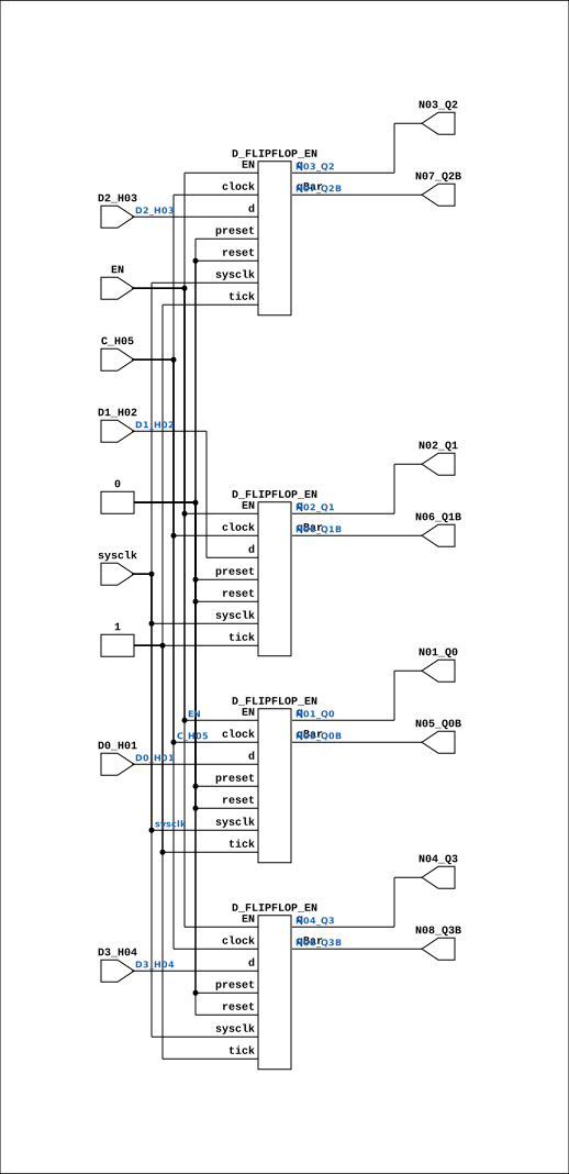
Contains: D_FLIPFLOP_EN x4
Module hierarchy - All modules
Schematic
Drawn from the Verilog: the yosys netlist of the Simulation (Verilator) build, instance CORE.CPU_BOARD.IO.DCD.DGA.IDBS.A282. Sub-modules are boxes (click the picture to open it full size; there every sub-module box links to its page, and every wire shows its Verilog name).
Description
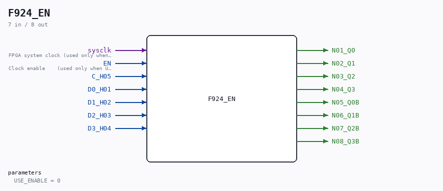
ND120 Shared F924_EN - F924 (NEC 4-bit D-type flip-flop) with an optional clock-enable mode. USE_ENABLE=0 (default): wraps the original F924 - posedge C_H05, original behaviour. USE_ENABLE=1: posedge sysclk, captures when EN is high (P2 clock- domain conversion mode - see SCAN_FF_EN.v / the plan doc). This branch is a STRUCTURAL COPY of the original F924 body - every wire and assign identical - with only the four internal flops swapped from D_FLIPFLOP #(.InvertClockEnable(0)) to D_FLIPFLOP_EN #(.USE_ENABLE(1)) (default ASYNC_RESET=0; the originals tie preset/reset to 0 and tick to 1, preserved here). The C_H05 pin is routed to the flops' (unused-in-mode-1) clock pins. Last reviewed: 10-JUL-2026 Ronny Hansen
Parameters
| Parameter | Default |
|---|---|
USE_ENABLE |
0 |
Ports
| Direction | Width | Name | Description |
|---|---|---|---|
| input | 1 |
sysclk |
FPGA system clock (used only when USE_ENABLE=1) |
| input | 1 |
EN |
Clock enable (used only when USE_ENABLE=1) |
| input | 1 |
C_H05 |
|
| input | 1 |
D0_H01 |
|
| input | 1 |
D1_H02 |
|
| input | 1 |
D2_H03 |
|
| input | 1 |
D3_H04 |
|
| output | 1 |
N01_Q0 |
|
| output | 1 |
N02_Q1 |
|
| output | 1 |
N03_Q2 |
|
| output | 1 |
N04_Q3 |
|
| output | 1 |
N05_Q0B |
|
| output | 1 |
N06_Q1B |
|
| output | 1 |
N07_Q2B |
|
| output | 1 |
N08_Q3B |
Verilog source
Verilog/Shared/ndlib/F924_EN.v on GitHub.
Show the Verilog of F924_EN (173 lines)
/**************************************************************************
** ND120 Shared                                                          **
**                                                                       **
** F924_EN - F924 (NEC 4-bit D-type flip-flop) with an optional          **
** clock-enable mode.                                                    **
**                                                                       **
** USE_ENABLE=0 (default): wraps the original F924 - posedge C_H05,      **
**   original behaviour.                                                 **
** USE_ENABLE=1: posedge sysclk, captures when EN is high (P2 clock-     **
**   domain conversion mode - see SCAN_FF_EN.v / the plan doc). This     **
**   branch is a STRUCTURAL COPY of the original F924 body - every       **
**   wire and assign identical - with only the four internal flops       **
**   swapped from D_FLIPFLOP #(.InvertClockEnable(0)) to                 **
**   D_FLIPFLOP_EN #(.USE_ENABLE(1)) (default ASYNC_RESET=0; the         **
**   originals tie preset/reset to 0 and tick to 1, preserved here).     **
**   The C_H05 pin is routed to the flops' (unused-in-mode-1) clock      **
**   pins.                                                               **
**                                                                       **
** Last reviewed: 10-JUL-2026                                            **
** Ronny Hansen                                                          **
***************************************************************************/

module F924_EN #(
    parameter integer USE_ENABLE = 0
) (
    input sysclk,  //! FPGA system clock (used only when USE_ENABLE=1)
    input EN,      //! Clock enable    (used only when USE_ENABLE=1)

    // Clock (used only when USE_ENABLE=0)
    input C_H05,

    // Data inputs
    input D0_H01,
    input D1_H02,
    input D2_H03,
    input D3_H04,

    // Normal outputs
    output N01_Q0,
    output N02_Q1,
    output N03_Q2,
    output N04_Q3,

    // Negated outputs
    output N05_Q0B,
    output N06_Q1B,
    output N07_Q2B,
    output N08_Q3B
);

  generate
    if (USE_ENABLE == 1) begin : gen_enable

      /*******************************************************************************
       ** The wires are defined here (structural copy of F924)                       **
       *******************************************************************************/
      wire s_clock;
      wire s_d0;
      wire s_d1;
      wire s_d2;
      wire s_d3;
      wire s_q0_n;
      wire s_q0;
      wire s_q1_n;
      wire s_q1;
      wire s_q2_n;
      wire s_q2;
      wire s_q3_n;
      wire s_q3;

      // Assign inputs
      assign s_clock = C_H05;

      assign s_d0 = D0_H01;
      assign s_d1 = D1_H02;
      assign s_d2 = D2_H03;
      assign s_d3 = D3_H04;

      // Assign outputs
      assign N01_Q0 = s_q0;
      assign N02_Q1 = s_q1;
      assign N03_Q2 = s_q2;
      assign N04_Q3 = s_q3;
      assign N05_Q0B = s_q0_n;
      assign N06_Q1B = s_q1_n;
      assign N07_Q2B = s_q2_n;
      assign N08_Q3B = s_q3_n;

      // The four internal flops, swapped to D_FLIPFLOP_EN in mode 1.
      // Originals were D_FLIPFLOP #(.InvertClockEnable(0)) with
      // preset/reset tied 0 and tick tied 1 (D_FLIPFLOP_EN defaults:
      // ASYNC_RESET=0; its mode-0 branch also uses InvertClockEnable(0)).
      // The clock pin (s_clock) is unused inside D_FLIPFLOP_EN when
      // USE_ENABLE=1 and is lint-waived there.
      D_FLIPFLOP_EN #(
          .USE_ENABLE(1)
      ) MEMORY_1 (
          .sysclk(sysclk),
          .EN(EN),
          .clock(s_clock),
          .d(s_d0),
          .preset(1'b0),
          .q(s_q0),
          .qBar(s_q0_n),
          .reset(1'b0),
          .tick(1'b1)
      );

      D_FLIPFLOP_EN #(
          .USE_ENABLE(1)
      ) MEMORY_2 (
          .sysclk(sysclk),
          .EN(EN),
          .clock(s_clock),
          .d(s_d1),
          .preset(1'b0),
          .q(s_q1),
          .qBar(s_q1_n),
          .reset(1'b0),
          .tick(1'b1)
      );

      D_FLIPFLOP_EN #(
          .USE_ENABLE(1)
      ) MEMORY_3 (
          .sysclk(sysclk),
          .EN(EN),
          .clock(s_clock),
          .d(s_d2),
          .preset(1'b0),
          .q(s_q2),
          .qBar(s_q2_n),
          .reset(1'b0),
          .tick(1'b1)
      );

      D_FLIPFLOP_EN #(
          .USE_ENABLE(1)
      ) MEMORY_4 (
          .sysclk(sysclk),
          .EN(EN),
          .clock(s_clock),
          .d(s_d3),
          .preset(1'b0),
          .q(s_q3),
          .qBar(s_q3_n),
          .reset(1'b0),
          .tick(1'b1)
      );

    end else begin : gen_orig
      /* verilator lint_off UNUSEDSIGNAL */
      wire unused_sys = sysclk & EN;
      /* verilator lint_on UNUSEDSIGNAL */
      F924 FF4 (
          .C_H05  (C_H05),
          .D0_H01 (D0_H01),
          .D1_H02 (D1_H02),
          .D2_H03 (D2_H03),
          .D3_H04 (D3_H04),
          .N01_Q0 (N01_Q0),
          .N02_Q1 (N02_Q1),
          .N03_Q2 (N03_Q2),
          .N04_Q3 (N04_Q3),
          .N05_Q0B(N05_Q0B),
          .N06_Q1B(N06_Q1B),
          .N07_Q2B(N07_Q2B),
          .N08_Q3B(N08_Q3B)
      );
    end
  endgenerate

endmodule