TTL_74646
Source: Verilog/Shared/support/TTL_74646.v
Where it sits (Simulation): ND120_TOP > ND120_CORE > ND3202D > BIF_5 > BIF_DPATH_9 > BIF_DPATH_CDLBD_11 > TTL_74646
- instance path: CORE.CPU_BOARD.BIF.DPATH.CDLBD.CHIP_7B
Used in: BIF_DPATH_CDLBD_11 (all tops)
Contains: no other modules.
Module hierarchy - All modules
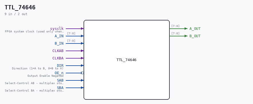
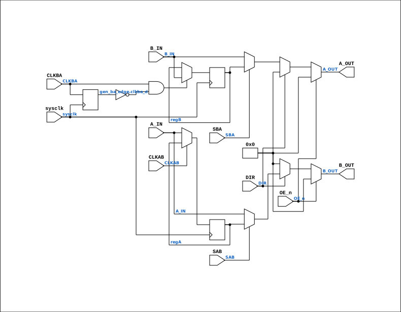
Schematic
Drawn from the Verilog: the yosys netlist of the Simulation (Verilator) build, instance CORE.CPU_BOARD.BIF.DPATH.CDLBD.CHIP_7B. Sub-modules are boxes (click the picture to open it full size; there every sub-module box links to its page, and every wire shows its Verilog name).
Description
Component : TTL_74646 OCTAL BUS TRANSCEIVERS AND REGISTERS WITH 3-STATE OUTPUTS (None inverting) DOC: https://www.ti.com/lit/ds/symlink/sn54as646.pdf Last reviewed: 14-DEC-2024 Ronny Hansen
Ports
| Direction | Width | Name | Description |
|---|---|---|---|
| input | 1 |
sysclk |
FPGA system clock (used only when USE_SYSCLK_AB/BA=2) |
| input | [7:0] |
A_IN |
|
| input | [7:0] |
B_IN |
|
| input | 1 |
CLKAB |
|
| input | 1 |
CLKBA |
|
| input | 1 |
DIR |
Direction (1=A to B, 0=B to A) |
| input | 1 |
OE_n (active low) |
Output Enable Negated |
| input | 1 |
SAB |
Select-Control AB - multiplex stored and real-time (transparent mode) registeres |
| input | 1 |
SBA |
Select-Control BA - multiplex stored and real-time (transparent mode) registeres. 0=REAL-TIME |
| output | [7:0] |
A_OUT |
|
| output | [7:0] |
B_OUT |
Verilog source
Verilog/Shared/support/TTL_74646.v on GitHub.
Show the Verilog of TTL_74646 (166 lines)
/******************************************************************************
 **                                                                          **
 ** Component : TTL_74646                                                    **
 **                                                                          **
 ** OCTAL BUS TRANSCEIVERS AND REGISTERS WITH 3-STATE OUTPUTS                **
 ** (None inverting)                                                         **
 **                                                                          **
 ** DOC: https://www.ti.com/lit/ds/symlink/sn54as646.pdf                     **
**                                                                           **
 ** Last reviewed: 14-DEC-2024                                               **
 ** Ronny Hansen                                                             **
 *****************************************************************************/

module TTL_74646(
   input sysclk, // FPGA system clock (used only when USE_SYSCLK_AB/BA=2)
   input[7:0] A_IN,
   input[7:0] B_IN,
   input CLKAB,
   input CLKBA,
   input DIR,   // Direction (1=A to B, 0=B to A)
   input OE_n,  // Output Enable Negated
   input SAB,   // Select-Control AB - multiplex stored and real-time (transparent mode) registeres
   input SBA,   // Select-Control BA - multiplex stored and real-time (transparent mode) registeres. 0=REAL-TIME

   output[7:0] A_OUT,
   output[7:0] B_OUT
);

   // USE_SYSCLK_AB / USE_SYSCLK_BA select how the two internal registers
   // capture (independently, one per clock pin):
   //   0 (default): original posedge CLKAB / CLKBA - matches the real chip.
   //   2: sysclk-sampled RISING-EDGE capture (AM29C821 USE_SYSCLK=2
   //      pattern) - the FPGA-safe mode when the clock pin is driven by a
   //      control strobe (ECREQ, BGNT_n ...), not a clock. One capture per
   //      detected rise, no fabric-routed clock net. NOTE: the capture
   //      lands one sysclk AFTER the rise - only safe when the data is
   //      still valid then (start-of-window strobes like ECREQ).
   //   3: sysclk WINDOWED capture - follow the data on every posedge
   //      sysclk while the strobe pin is LOW, hold from the rise on. Ends
   //      holding the value present AT the strobe rise, with no one-cycle
   //      lag - the FPGA-safe mode for END-of-window strobes (DSTB_n,
   //      which marks the end of the memory data window; mode 2 sampled
   //      one cycle late, after the memory stopped driving). Only valid
   //      when the register is not observed during the low window (CDLBD:
   //      SAB=DSTB_n selects real-time data while the strobe is low, so
   //      regA is only read after the rise).
   parameter USE_SYSCLK_AB = 0;
   parameter USE_SYSCLK_BA = 0;


   /*******************************************************************************
   ** The wires are defined here                                                 **
   *******************************************************************************/
   wire s_sab;
   wire s_clkab;
   wire s_sba;
   wire s_clkba;
   wire s_dir;
   wire s_oe_n;


   /*******************************************************************************
   ** The module functionality is described here                                 **
   *******************************************************************************/

   /*******************************************************************************
   ** Here all input connections are defined                                     **
   *******************************************************************************/
   assign s_sab   = SAB;
   assign s_clkab = CLKAB;
   assign s_sba   = SBA;
   assign s_clkba = CLKBA;
   assign s_dir   = DIR;
   assign s_oe_n  = OE_n;


   /*******************************************************************************
   ** Here all in-lined components are defined                                   **
   *******************************************************************************/

   reg [7:0] regA;
   reg [7:0] regB;

   reg [7:0] regA_Delayed;
   reg [7:0] regB_Delayed;


   always@(A_IN)
   begin
      regA_Delayed <= A_IN;
   end

   always@(B_IN, SBA)
   begin
      regB_Delayed <= B_IN;
   end

   generate
      if (USE_SYSCLK_AB == 2) begin : gen_ab_edge
         reg clkab_d = 1'b0;
         always @(posedge sysclk) begin
            clkab_d <= s_clkab;
            if (s_clkab && !clkab_d) regA <= regA_Delayed;
         end
      end else if (USE_SYSCLK_AB == 3) begin : gen_ab_window
         always @(posedge sysclk) begin
            if (!s_clkab) regA <= regA_Delayed;
         end
      end else begin : gen_ab_posedge
         always @(posedge s_clkab )
         begin
            //regA <= A_IN; //Capture directly input signal
            regA <= regA_Delayed; //Capture delayed input signal
         end
      end

      if (USE_SYSCLK_BA == 2) begin : gen_ba_edge
         reg clkba_d = 1'b0;
         always @(posedge sysclk) begin
            clkba_d <= s_clkba;
            if (s_clkba && !clkba_d) regB <= regB_Delayed;
         end
      end else begin : gen_ba_posedge
         always @(posedge s_clkba )
         begin
            //regB <= B_IN;  //Capture directly input signal
            regB <= regB_Delayed; //Capture delayed input signal
         end
      end
   endgenerate


/*
A_OUT:
   If OE_n is not active (low), the output is 0.

   If DIR is 0 (B to A direction):
      If SBA is 0, A_OUT gets real-time data from B_IN.
      If SBA is 1, A_OUT gets stored data from regB.

*/
   // sdir = 0 => B => A

   // s_sba = 0 => Real Time B to A
   // s_sba = 1 => Register  B to A
   assign A_OUT = s_oe_n ? 8'b0 : !s_dir ?  ((!s_sba) ? B_IN : regB) : 8'b0;


/*
B_OUT:
      If OE_n is not active (low), the output is 0.

      If DIR is 1 (A to B direction):
         If SAB is 0, B_OUT gets real-time data from A_IN.
         If SAB is 1, B_OUT gets stored data from regA.
*/

   // sdir = 1 => A => B

   // s_sab = 0 => Real Time A to B
   // s_sab = 1 => Register  A to B
   assign B_OUT = s_oe_n ? 8'b0 : s_dir ?  ((!s_sab) ? A_IN : regA) : 8'b0;

endmodule