SIP1M9
Source: Verilog/Shared/support/SIP1M9.v
Hierarchy: not instantiated by any of the 9 build tops (elaborated by yosys).
Module hierarchy - All modules
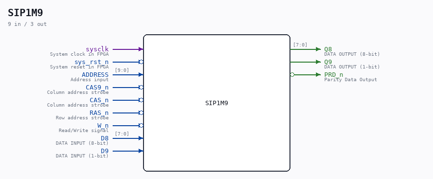
Schematic
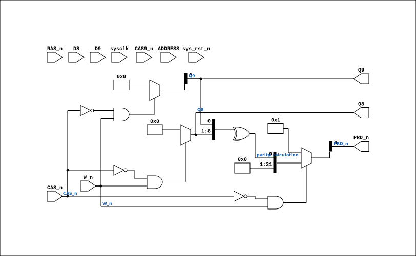
Drawn from the Verilog: no build top uses this module, so it was elaborated from its own file with no defines and default parameters. Sub-modules are boxes (click the picture to open it full size; there every sub-module box links to its page, and every wire shows its Verilog name).
Description
RAM CHIP 1 MBYTE (1024KB) This ram has PARITY bit.. THM91020 - http://norsk-data.com/library/libother/extern/THM91020.pdf THM91070 - http://norsk-data.com/library/libother/extern/THM91070.pdf Last reviewed: 9-FEB-2025 Ronny Hansen
Ports
| Direction | Width | Name | Description |
|---|---|---|---|
| input | 1 |
sysclk |
System clock in FPGA |
| input | 1 |
sys_rst_n (active low) |
System reset in FPGA |
| input | [9:0] |
ADDRESS |
Address input |
| input | 1 |
CAS9_n (active low) |
Column address strobe |
| input | 1 |
CAS_n (active low) |
Column address strobe |
| input | 1 |
RAS_n (active low) |
Row address strobe |
| input | 1 |
W_n (active low) |
Read/Write signal |
| input | [7:0] |
D8 |
DATA INPUT (8-bit) |
| input | 1 |
D9 |
DATA INPUT (1-bit) |
| output | [7:0] |
Q8 |
DATA OUTPUT (8-bit) |
| output | 1 |
Q9 |
DATA OUTPUT (1-bit) |
| output | 1 |
PRD_n (active low) |
Parity Data Output |
Verilog source
Verilog/Shared/support/SIP1M9.v on GitHub.
Show the Verilog of SIP1M9 (227 lines)
/******************************************************************************
** RAM CHIP 1 MBYTE (1024KB)                                                  **
**                                                                            **
** This ram has PARITY bit..                                                  **
** THM91020 - http://norsk-data.com/library/libother/extern/THM91020.pdf      **
** THM91070 - http://norsk-data.com/library/libother/extern/THM91070.pdf      **
**                                                                            **
** Last reviewed: 9-FEB-2025                                                  **
** Ronny Hansen                                                               **
********************************************************************************/

// TODO: Implement access to real RAM inside FPGA

module SIP1M9 (

    // Input signals
    input sysclk,    //! System clock in FPGA
    input sys_rst_n, //! System reset in FPGA

    input [9:0] ADDRESS,  //! Address input
    input       CAS9_n,   //! Column address strobe
    input       CAS_n,    //! Column address strobe
    input       RAS_n,    //! Row address strobe
    input       W_n,      //! Read/Write signal


    // Input signals
    input [7:0] D8,  //! DATA INPUT (8-bit)
    input       D9,  //! DATA INPUT (1-bit)

    // Output signals
    output [7:0] Q8,    //! DATA OUTPUT (8-bit)
    output       Q9,    //! DATA OUTPUT (1-bit)
    output       PRD_n  //! Parity Data Output

);

  wire parity_calculation;

  // Parameters are declared here
  parameter ramSize = 0; // 0 = Disabled, 1=64KB, 2=1MB, 3=4KB (for FPGA BRAM testing)


// Convert ramSize into a memory depth.
// Feel free to tweak default 1 if "disabled" should do something else.
  localparam integer MEM_DEPTH = (ramSize == 2) ? 1048575 :   // 1 MB (too large for FPGA BRAM)
                                 (ramSize == 1) ? 65535   :   // 64 KB (still too large for small FPGAs)
                                 (ramSize == 3) ? 4095    :   // 4 KB (fits in BRAM for testing)
                                                  1;          // Disabled = 1 word (or 0, if desired)

  reg  [7:0] reg_Q8;
  reg        reg_Q9;

  // NOTE: sdram/sdram_9 are declared at MODULE scope (not inside the generate) so
  // their Verilator hierarchical name stays `...CHIP_15H__DOT__sdram`, which the C++
  // sim harnesses (loadfile in test_nd120.cpp / Run120.cpp / latch_ff_compare.cpp)
  // reference to preload programs. ONLY declared for Verilator (ramSize=2 DRAM model);
  // on the FPGA (ramSize=3) it is unused, and as a block-RAM-styled array it was NOT
  // pruned in time and pushed BRAM usage over the xc7a35t's 100-block limit -> synth
  // OOM. Guarded out of the FPGA build. (ramSize=2 <=> VERILATOR_SIM in this design.)
`ifdef VERILATOR_SIM
  (* ram_style = "block" *) reg [7:0] sdram   [0:MEM_DEPTH-1];
  // No sdram_9: parity is regenerated on read, never stored (see the policy
  // note below). Nothing outside this file referenced it.
`endif

generate
if (ramSize == 3) begin : g_fpga_bram
  // ======================================================================
  //  FPGA SYNCHRONOUS BRAM PATH (ramSize=3)
  // ----------------------------------------------------------------------
  //  The original DRAM model below (ramSize=2) is a ZERO-DELAY simulation
  //  model: it clocks on negedge RAS_n/CAS_n (routed control signals, not a
  //  clock), gates the read output combinationally by CAS_n, and indexes a
  //  20-bit `sip_address` into whatever depth is declared. On real BRAM that
  //  fails four ways (glitchy clock, read-0 race, address-changes-with-clock,
  //  and — because sip_address = {row,col} reorders the bits — consecutive
  //  addresses land 1024 apart and alias in a small array).
  //
  //  This path is a proper SYNCHRONOUS BRAM: everything on sysclk; RAS_n/CAS_n
  //  are treated as level enables (they are PAL outputs registered on OSC=sysclk
  //  in this design, so they are already sysclk-synchronous); the read output is
  //  registered and HELD stable (the controller's RDATA strobe samples it late in
  //  the cycle while CAS is still low); and the address is reconstructed to the
  //  LINEAR word address LBD[19:0] = {col, row} so it is contiguous, then the low
  //  FPGA_ADDR_BITS are used (no reorder-aliasing).
  // ======================================================================
  localparam integer FPGA_ADDR_BITS = 12;                 // 4 K words/chip (fits xc7a35t; tune up later)
  localparam integer FPGA_DEPTH     = (1 << FPGA_ADDR_BITS);

  (* ram_style = "block" *) reg [7:0] bram8 [0:FPGA_DEPTH-1];

  // PARITY (D9 / Q9): COMPUTED ON READ, NEVER STORED
  // -------------------------------------------------------------------------
  // POLICY (Ronny, 3-AUG-2026): no FPGA target stores parity - not here, not in
  // any other sheet-49 backend. One bit per word still costs a whole RAMB18 per
  // chip (the smallest block Vivado can allocate), i.e. 6 RAMB18 across the six
  // chips to hold 4 Kbit, and the ND-120 never needs the STORED bit: what the
  // board consumes is a word whose parity is CONSISTENT with its data.
  //
  // So D9 is accepted and dropped on write, and Q9 is regenerated on read as
  // ODD parity of the byte actually returned: PAR = ~^D8, the Am29833A
  // convention (AM29833A.v:100 generates ~(^R); :116 flags an error when the
  // 9-bit group comes out EVEN). That keeps PRD_n - and MEM_RAM_49's CORR_n -
  // reading "correct", and it is what MEM_RAM_49_SDRAM already does on Tang.
  //
  // Returning 0 here (what this path did until 3-AUG-2026) was NOT neutral: it
  // is the wrong parity for every byte with even population, so unmasking
  // LPERR_n would have faulted about half of all reads.

  reg  [9:0] row_addr;                                     // AA captured at the RAS falling edge
  reg        ras_n_d;                                      // RAS_n one sysclk ago (edge detect)
  // Linear word address = {col, row} = LBD[19:0]; use the low FPGA_ADDR_BITS.
  wire [19:0] lin_addr  = {ADDRESS[9:0], row_addr[9:0]};   // {col(on AA while both low), row}
  wire [FPGA_ADDR_BITS-1:0] a = lin_addr[FPGA_ADDR_BITS-1:0];

  reg cas_win_d;  // both-low window, one sysclk delayed (first-edge detect)
  reg [7:0] d8_q;  // write data captured BEFORE CAS (see comment below)
  reg       d9_q;

  always @(posedge sysclk) begin
    ras_n_d <= RAS_n;
    // Capture the ROW ONLY at the RAS falling edge. Verified against the real
    // controller (DBG_MEM trace): AA carries the row exactly at RAS-fall; the very
    // next sysclk (RAS still low, CAS still HIGH) AA already switches to the COLUMN,
    // so a level-triggered latch grabbed the column and every access hit {col,col}.
    if (ras_n_d && !RAS_n) row_addr <= ADDRESS[9:0];

    // Write-data capture: on silicon the D bus is driven BEFORE CAS-fall and
    // released shortly after it (measured on the Tang SDRAM backend,
    // 8-JUL-2026; the zero-delay sim's "valid at CAS-fall" is the PRE-edge
    // value). Capture every sysclk while RAS is active and CAS not yet seen:
    // the final capture (the CAS-fall edge) holds the settled cycle-N+1 value.
    if (!RAS_n && CAS_n) begin
      d8_q <= D8;
      d9_q <= D9;
    end

    // Access while both strobes are active (bank-gated CAS_n already selects us);
    // AA carries the column throughout the both-low window.
    cas_win_d <= (!RAS_n && !CAS_n);
    if (!RAS_n && !CAS_n) begin
      if (W_n) begin                                       // read (re-reads while CAS low; addr stable)
        reg_Q8 <= bram8[a];
        reg_Q9 <= ~(^bram8[a]);                            // ODD parity, regenerated
      end else if (!cas_win_d) begin                       // write ONCE, first both-low
        bram8[a] <= d8_q;                                  // edge, with the pre-CAS
      end                                                  // captured data (D9 dropped)
    end
  end

  // Registered, held read data; still bank-gated (0 when not selected / not a read)
  // so the three banks' outputs OR-combine correctly in MEM_RAM_49.
  assign Q8 = ((CAS_n == 0) && (W_n)) ? reg_Q8 : 8'b0;
  assign Q9 = ((CAS_n == 0) && (W_n)) ? reg_Q9 : 1'b0;

end else begin : g_sim_dram
  // ======================================================================
  //  ORIGINAL ZERO-DELAY DRAM MODEL (ramSize=2 Verilator, etc.) — unchanged
  //  (sdram/sdram_9 declared at module scope above)
  // ======================================================================
  reg [9:0] hi_address;

  wire [19:0] sip_address = (CAS_n == 0) ? {hi_address[9:0], ADDRESS[9:0]} : 20'b0;

  always @(negedge RAS_n) begin
    hi_address <= ADDRESS[9:0];
  end

`ifdef DBG_MEM
  // Ground-truth timing capture of the working DRAM model vs sysclk, to design the
  // FPGA sync BRAM. Logs the AA at each RAS/CAS fall and the sysclk-level view.
  integer dbg_cyc = 0;
  always @(posedge sysclk) dbg_cyc <= dbg_cyc + 1;
  always @(negedge RAS_n) $display("MEM RASfall cyc=%0d AA(row)=%o", dbg_cyc, ADDRESS);
  always @(negedge CAS_n) if (!RAS_n)
    $display("MEM CASfall cyc=%0d AA(col)=%o row=%o W_n=%b D8=%o", dbg_cyc, ADDRESS, hi_address, W_n, D8);
  always @(posedge sysclk) if (!RAS_n || !CAS_n)
    $display("MEM sclk   cyc=%0d RAS_n=%b CAS_n=%b AA=%o W_n=%b", dbg_cyc, RAS_n, CAS_n, ADDRESS, W_n);
`endif

  always @(negedge CAS_n) begin
`ifdef VERILATOR_SIM
    // sdram/sdram_9 exist only under VERILATOR_SIM; this whole DRAM model branch is
    // never GENERATED on the FPGA (ramSize=3 -> g_fpga_bram) but Vivado still PARSES
    // it, so the sdram references must be preprocessed out for the FPGA build.
    if (!RAS_n) begin
      if (W_n) begin  // read
        reg_Q8 <= sdram[sip_address];
        // Parity regenerated, never stored - same rule as the FPGA path above,
        // so the Verilator reference and silicon cannot diverge here.
        reg_Q9 <= ~(^sdram[sip_address]);
      end else begin  // write
        sdram[sip_address] <= D8;                      // D9 accepted and dropped
      end
    end
`endif
  end

  // Data out is valid as long as CAS is active (and its read, not write)
  assign Q8 = ((CAS_n == 0) && (W_n)) ? reg_Q8 : 8'b00000000;
  assign Q9 = ((CAS_n == 0) && (W_n)) ? reg_Q9 : 0;
end
endgenerate


  // Even Parity Logic
    // ^ (in Verilig) is XOR giving 0=if even, 1=if odd.
  // Invert this so that the PAR signal is according to Am29833A documentation: PAR=L on ODD and PAR=H on EVEN
  assign parity_calculation =  (^{Q8, Q9});

  assign PRD_n = ((CAS_n == 0) && (W_n))  ? parity_calculation : 1;
  /*
  assign PRD_n = ~(
    Q8[0] ^
    Q8[1] ^
    Q8[2] ^
    Q8[3] ^
    Q8[4] ^
    Q8[5] ^
    Q8[6] ^
    Q8[7] ^
    Q9
  );
  */

endmodule