AM29841
Source: Verilog/Shared/support/AM29841.v
Where it sits (Simulation): ND120_TOP > ND120_CORE > ND3202D > CPU_15 > CPU_PROC_32 > AM29841
- instance path: CORE.CPU_BOARD.CPU.PROC.CHIP_25F
Used in: CPU_PROC_32 (all tops)
Contains: no other modules.
Module hierarchy - All modules
Schematic
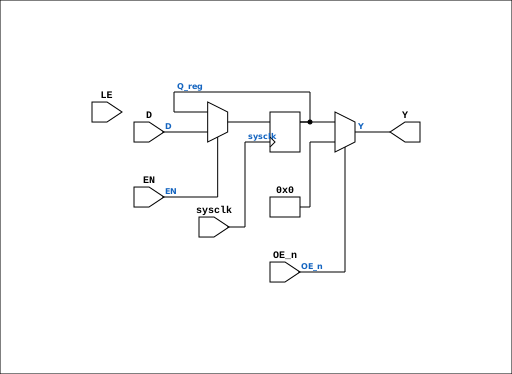
Drawn from the Verilog: the yosys netlist of the Simulation (Verilator) build, instance CORE.CPU_BOARD.CPU.PROC.CHIP_25F. Sub-modules are boxes (click the picture to open it full size; there every sub-module box links to its page, and every wire shows its Verilog name).
Description
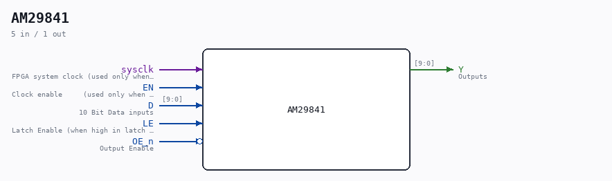
ND120 Shared Component AM29841 Bus Driver 10 bit (D-Latch) with 3-state output Documentation: https://www.alldatasheet.com/datasheet-pdf/pdf/107079/AMD/AM29841.html Last reviewed: 1-DEC-2024 Ronny Hansen
Ports
| Direction | Width | Name | Description |
|---|---|---|---|
| input | 1 |
sysclk |
FPGA system clock (used only when USE_ENABLE=1) |
| input | 1 |
EN |
Clock enable (used only when USE_ENABLE=1) |
| input | [9:0] |
D |
10 Bit Data inputs |
| input | 1 |
LE |
Latch Enable (when high in latch mode, rising edge in FF mode) |
| input | 1 |
OE_n (active low) |
Output Enable |
| output | [9:0] |
Y |
Outputs |
Verilog source
Verilog/Shared/support/AM29841.v on GitHub.
Show the Verilog of AM29841 (74 lines)
/**********************************************************************************************************
** ND120 Shared                                                                                          **
**                                                                                                       **
** Component AM29841                                                                                     **
**                                                                                                       **
** Bus Driver 10 bit (D-Latch) with 3-state output                                                       **
** Documentation: https://www.alldatasheet.com/datasheet-pdf/pdf/107079/AMD/AM29841.html                 **
**                                                                                                       **
** Last reviewed: 1-DEC-2024                                                                             **
** Ronny Hansen                                                                                          **
***********************************************************************************************************/

module AM29841 (
    input wire sysclk,    // FPGA system clock (used only when USE_ENABLE=1)
    input wire EN,        // Clock enable     (used only when USE_ENABLE=1)
    input wire [9:0] D,   // 10 Bit Data inputs
    input wire LE,        // Latch Enable (when high in latch mode, rising edge in FF mode)
    input wire OE_n,      // Output Enable
    output wire [9:0] Y   // Outputs
);

    // FPGA_MODE: Set to 1 for edge-triggered operation (FPGA synthesis)
    //            Set to 0 for transparent latch operation (original behavior)
`ifdef USE_TRANSPARENT_LATCHES
    parameter FPGA_MODE = 0;  // Simulation: use transparent latch (original behavior)
`else
    parameter FPGA_MODE = 1;  // FPGA: use edge-triggered FF for synthesis
`endif

    // USE_ENABLE=1: capture on posedge sysclk when EN is high (rise-aligned
    // enable for the clock that drives LE) instead of clocking on the routed
    // LE net (P3, docs/plan-fix-unconstrained-clocks.md). Overrides FPGA_MODE.
    parameter USE_ENABLE = 0;

    reg [9:0] Q_reg = 10'b0;  // Internal register/latch with initial value for FPGA

    generate
        if (USE_ENABLE == 1) begin : gen_enable
            /* verilator lint_off UNUSEDSIGNAL */
            wire unused_le = LE;
            /* verilator lint_on UNUSEDSIGNAL */
            always @(posedge sysclk) begin
                if (EN) Q_reg <= D;
            end
        end else if (FPGA_MODE == 1) begin : gen_flipflop
            /* verilator lint_off UNUSEDSIGNAL */
            wire unused_sys = sysclk & EN;
            /* verilator lint_on UNUSEDSIGNAL */
            // Edge-triggered flip-flop mode (FPGA-friendly)
            always @(posedge LE) begin
                Q_reg <= D;  // Capture on rising edge
            end
        end else begin : gen_latch
            /* verilator lint_off UNUSEDSIGNAL */
            wire unused_sys = sysclk & EN;
            /* verilator lint_on UNUSEDSIGNAL */
            // Transparent latch mode (original behavior)
            /* verilator lint_off LATCH */
            always @(*) begin
                if (LE)
                    Q_reg = D; // Transparent mode: follows input when LE high
                else
                    Q_reg = Q_reg; // Hold previous value
            end
            /* verilator lint_on LATCH */
        end
    endgenerate

    // Output control
    // When OE_n is low (active), outputs reflect the registered data
    // When OE_n is high, outputs are in high-impedance state (zero for simulation)
    assign Y = OE_n ? 10'b0 : Q_reg;

endmodule