ND120_TOP
ND120 CPU, MEMORY MANAGEMENT and MEMORY.
Source: Verilog/ND120_TOP.v
· Author: Ronny Hansen
Where it sits (Simulation): ND120_TOP
Used in: nd120_cmod_top (Cmod)
Contains: BUFG (vendor) x2 (only on Basys3, Cmod), MMCME2_BASE (vendor) (only on Basys3, Cmod), ND120_CORE, nd_storage_devices (only on Simulation), nds_mem_model (only on Simulation), sd_card_model (only on Simulation), SevenSegDebug (only on Basys3, Cmod)
Module hierarchy - All modules
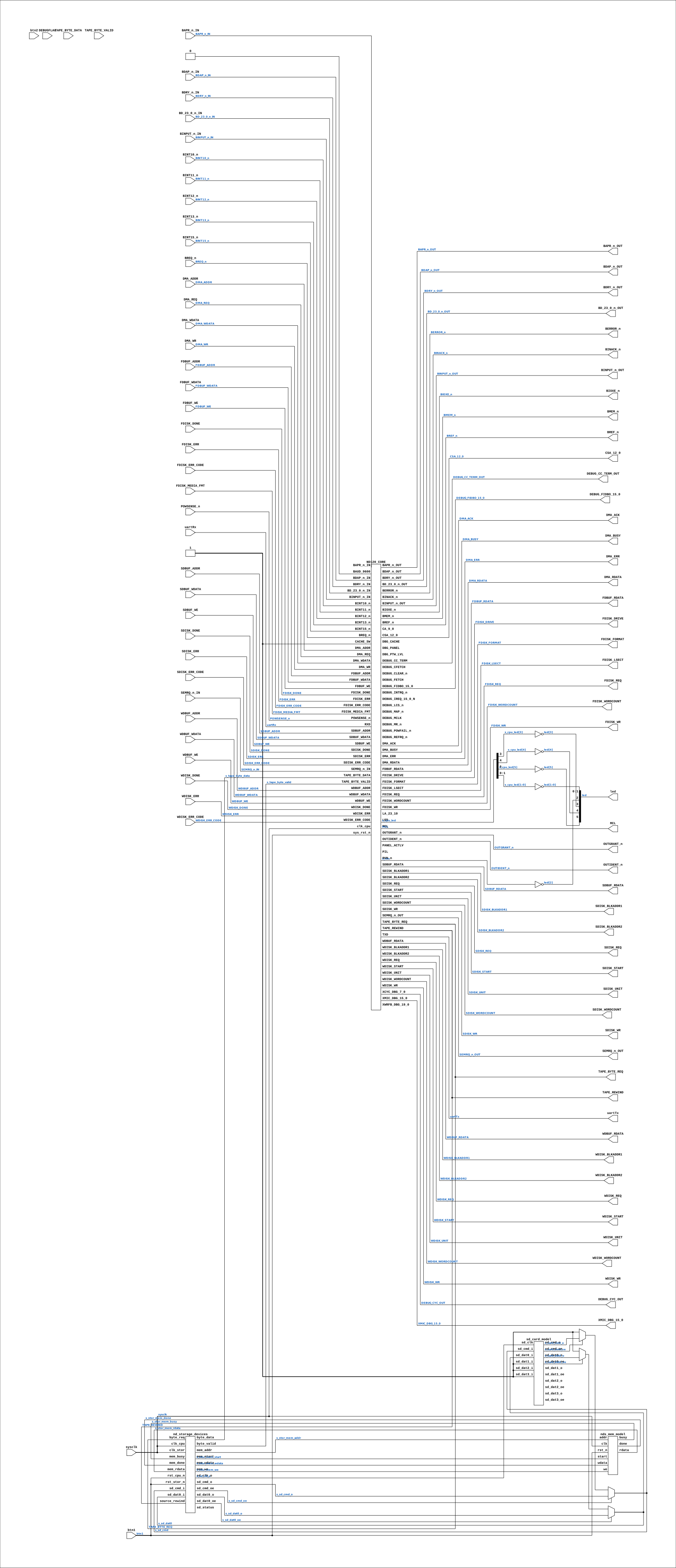
Schematic
Drawn from the Verilog: the yosys netlist of the Simulation (Verilator) build, where it is the top. Sub-modules are boxes (click the picture to open it full size; there every sub-module box links to its page, and every wire shows its Verilog name).
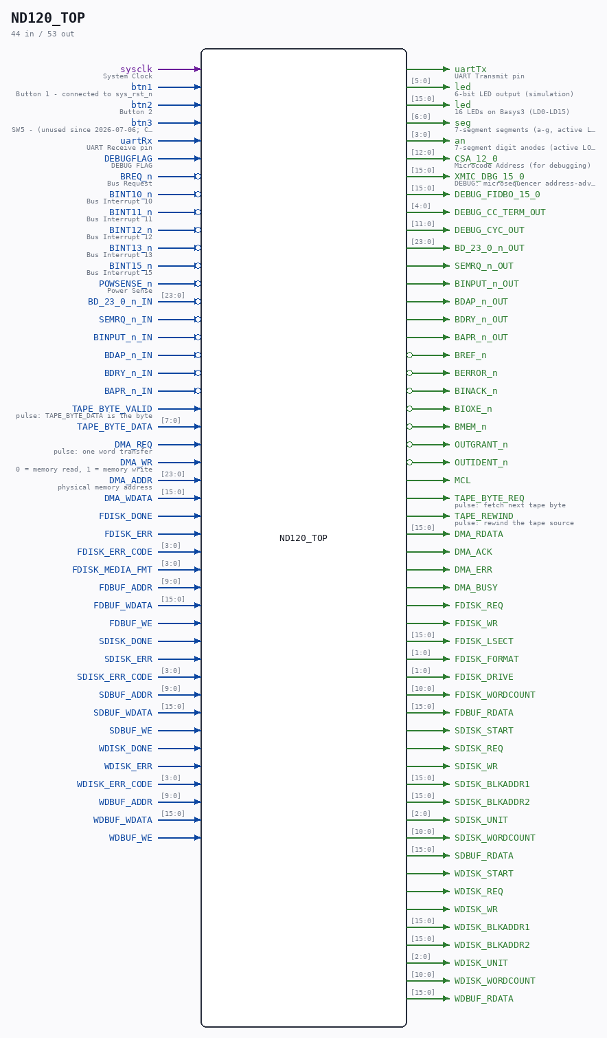
Ports
| Direction | Width | Name | Description |
|---|---|---|---|
| input | 1 |
sysclk |
System Clock |
| input | 1 |
btn1 |
Button 1 - connected to sys_rst_n |
| input | 1 |
btn2 |
Button 2 |
| input | 1 |
btn3 |
SW5 - (unused since 2026-07-06; CPU now fixed at clk_cpu ~16.67MHz) |
| input | 1 |
uartRx |
UART Receive pin |
| output | 1 |
uartTx |
UART Transmit pin |
| output | [5:0] |
led |
6-bit LED output (simulation) |
| output | [15:0] |
led |
16 LEDs on Basys3 (LD0-LD15) |
| output | [6:0] |
seg |
7-segment segments (a-g, active LOW) |
| output | [3:0] |
an |
7-segment digit anodes (active LOW) |
| input | 1 |
DEBUGFLAG |
DEBUG FLAG |
| output | [12:0] |
CSA_12_0 |
Microcode Address (for debugging) |
| output | [15:0] |
XMIC_DBG_15_0 |
DEBUG: microsequencer address-advance probe (matches Tang capture: {SC6,s_mclk_n,MCLK_EN,regIW[12:0]}) |
| output | [15:0] |
DEBUG_FIDBO_15_0 |
|
| output | [4:0] |
DEBUG_CC_TERM_OUT |
|
| output | [11:0] |
DEBUG_CYC_OUT |
|
| input | 1 |
BREQ_n (active low) |
Bus Request |
| input | 1 |
BINT10_n (active low) |
Bus Interrupt 10 |
| input | 1 |
BINT11_n (active low) |
Bus Interrupt 11 |
| input | 1 |
BINT12_n (active low) |
Bus Interrupt 12 |
| input | 1 |
BINT13_n (active low) |
Bus Interrupt 13 |
| input | 1 |
BINT15_n (active low) |
Bus Interrupt 15 |
| input | 1 |
POWSENSE_n (active low) |
Power Sense |
| input | [23:0] |
BD_23_0_n_IN |
|
| output | [23:0] |
BD_23_0_n_OUT |
|
| input | 1 |
SEMRQ_n_IN |
|
| output | 1 |
SEMRQ_n_OUT |
|
| input | 1 |
BINPUT_n_IN |
|
| output | 1 |
BINPUT_n_OUT |
|
| input | 1 |
BDAP_n_IN |
|
| output | 1 |
BDAP_n_OUT |
|
| input | 1 |
BDRY_n_IN |
|
| output | 1 |
BDRY_n_OUT |
|
| input | 1 |
BAPR_n_IN |
|
| output | 1 |
BAPR_n_OUT |
|
| output | 1 |
BREF_n (active low) |
|
| output | 1 |
BERROR_n (active low) |
|
| output | 1 |
BINACK_n (active low) |
|
| output | 1 |
BIOXE_n (active low) |
|
| output | 1 |
BMEM_n (active low) |
|
| output | 1 |
OUTGRANT_n (active low) |
|
| output | 1 |
OUTIDENT_n (active low) |
|
| output | 1 |
MCL |
|
| output | 1 |
TAPE_BYTE_REQ |
pulse: fetch next tape byte |
| input | 1 |
TAPE_BYTE_VALID |
pulse: TAPE_BYTE_DATA is the byte |
| input | [7:0] |
TAPE_BYTE_DATA |
|
| output | 1 |
TAPE_REWIND |
pulse: rewind the tape source |
| input | 1 |
DMA_REQ |
pulse: one word transfer |
| input | 1 |
DMA_WR |
0 = memory read, 1 = memory write |
| input | [23:0] |
DMA_ADDR |
physical memory address |
| input | [15:0] |
DMA_WDATA |
|
| output | [15:0] |
DMA_RDATA |
|
| output | 1 |
DMA_ACK |
|
| output | 1 |
DMA_ERR |
|
| output | 1 |
DMA_BUSY |
|
| output | 1 |
FDISK_REQ |
|
| output | 1 |
FDISK_WR |
|
| output | [15:0] |
FDISK_LSECT |
|
| output | [1:0] |
FDISK_FORMAT |
|
| output | [1:0] |
FDISK_DRIVE |
|
| output | [10:0] |
FDISK_WORDCOUNT |
|
| input | 1 |
FDISK_DONE |
|
| input | 1 |
FDISK_ERR |
|
| input | [3:0] |
FDISK_ERR_CODE |
|
| input | [3:0] |
FDISK_MEDIA_FMT |
|
| input | [9:0] |
FDBUF_ADDR |
|
| input | [15:0] |
FDBUF_WDATA |
|
| input | 1 |
FDBUF_WE |
|
| output | [15:0] |
FDBUF_RDATA |
|
| output | 1 |
SDISK_START |
|
| output | 1 |
SDISK_REQ |
|
| output | 1 |
SDISK_WR |
|
| output | [15:0] |
SDISK_BLKADDR1 |
|
| output | [15:0] |
SDISK_BLKADDR2 |
|
| output | [2:0] |
SDISK_UNIT |
|
| output | [10:0] |
SDISK_WORDCOUNT |
|
| input | 1 |
SDISK_DONE |
|
| input | 1 |
SDISK_ERR |
|
| input | [3:0] |
SDISK_ERR_CODE |
|
| input | [9:0] |
SDBUF_ADDR |
|
| input | [15:0] |
SDBUF_WDATA |
|
| input | 1 |
SDBUF_WE |
|
| output | [15:0] |
SDBUF_RDATA |
|
| output | 1 |
WDISK_START |
|
| output | 1 |
WDISK_REQ |
|
| output | 1 |
WDISK_WR |
|
| output | [15:0] |
WDISK_BLKADDR1 |
|
| output | [15:0] |
WDISK_BLKADDR2 |
|
| output | [2:0] |
WDISK_UNIT |
|
| output | [10:0] |
WDISK_WORDCOUNT |
|
| input | 1 |
WDISK_DONE |
|
| input | 1 |
WDISK_ERR |
|
| input | [3:0] |
WDISK_ERR_CODE |
|
| input | [9:0] |
WDBUF_ADDR |
|
| input | [15:0] |
WDBUF_WDATA |
|
| input | 1 |
WDBUF_WE |
|
| output | [15:0] |
WDBUF_RDATA |
Verilog source
Verilog/ND120_TOP.v on GitHub.
Show the Verilog of ND120_TOP (1345 lines)
// WaveDrom documentation: https://wavedrom.com/tutorial.html
// WaveDrom Editor: https://wavedrom.com/editor.html
// TerosHDL: see https://github.com/TerosTechnology/vscode-terosHDL
// Verible: https://github.com/chipsalliance/verible
// Verible plugin for VS Code: https://marketplace.visualstudio.com/items?itemName=CHIPSAlliance.verible
// Verible Lint: https://chipsalliance.github.io/verible/lint.html
// YoSys: https://github.com/YosysHQ/oss-cad-suite-build
/**************************************************************************
** ND120 CPU, MEMORY MANAGEMENT and MEMORY **
** **
** TOP LEVEL FOR FPGA IMPLEMENTATION **
** **
** Last reviewed: 22-MAR-2025 **
** Ronny Hansen **
***************************************************************************/
// Define USE_TRANSPARENT_LATCHES for latch behavior in PALs.
// Active when: VERILATOR_SIM is set (sim build) AND FPGA_FF_MODE is NOT set.
// This allows sim builds to test FF mode with: make compile USE_LATCHES=0
`ifdef VERILATOR_SIM
`ifndef FPGA_FF_MODE
`define USE_TRANSPARENT_LATCHES
`endif
`endif
//! @title ND120 CPU, MEMORY MANAGEMENT and MEMORY.
//! @author Ronny Hansen
//! TOP LEVEL FOR FPGA IMPLEMENTATION OF ND-3202D CPU BOARD
module ND120_TOP
(
// Core FPGA pins (always present)
input wire sysclk, //! System Clock
input wire btn1, //! Button 1 - connected to sys_rst_n
input wire btn2, //! Button 2
`ifndef VERILATOR_SIM
input wire btn3, //! SW5 - (unused since 2026-07-06; CPU now fixed at clk_cpu ~16.67MHz)
`endif
input wire uartRx, //! UART Receive pin
output wire uartTx, //! UART Transmit pin
`ifdef VERILATOR_SIM
output wire [5:0] led //! 6-bit LED output (simulation)
`else
output wire [15:0] led, //! 16 LEDs on Basys3 (LD0-LD15)
// 7-segment display (active LOW, Basys3)
output wire [6:0] seg, //! 7-segment segments (a-g, active LOW)
output wire [3:0] an //! 7-segment digit anodes (active LOW)
`endif
`ifdef VERILATOR_SIM
// Simulation-only ports: full bus interface for device emulation
,
input wire DEBUGFLAG, // DEBUG FLAG
output wire [12:0] CSA_12_0, //! Microcode Address (for debugging)
output wire [15:0] XMIC_DBG_15_0, //! DEBUG: microsequencer address-advance probe (matches Tang capture: {SC6,s_mclk_n,MCLK_EN,regIW[12:0]})
//! DEBUG: FIDBO, the internal data bus. Brought out as a PORT (01-SEP-2026)
//! because the wire alone is driven and never read, so Verilator optimises
//! it away and the C harness cannot reach it. Needed to read the PIE value
//! at microcode 001011 - the value the 001013 branch is decided on, and
//! where the MiSTer board first diverges from this boot.
output wire [15:0] DEBUG_FIDBO_15_0,
//! DEBUG: {TERM_n, CC3_n, CC2_n, CC1_n, CC0_n} - the condition and
//! terminate lines the microsequencer branches on. Brought out for the
//! same reason as FIDBO above: the MiSTer board reaches NOTI2 and fails to
//! leave it while the datapath values agree, which points at the CONDITION
//! rather than the data.
output wire [4:0] DEBUG_CC_TERM_OUT,
//! DEBUG: cycle-controller terminate-plane inputs (CYC_36.XCYC_DBG_7_0).
output wire [11:0] DEBUG_CYC_OUT,
// C-PLUG bus signals
input wire BREQ_n, // Bus Request
input wire BINT10_n, // Bus Interrupt 10
input wire BINT11_n, // Bus Interrupt 11
input wire BINT12_n, // Bus Interrupt 12
input wire BINT13_n, // Bus Interrupt 13
input wire BINT15_n, // Bus Interrupt 15
input wire POWSENSE_n, // Power Sense
// BUS data in/out
input wire [23:0] BD_23_0_n_IN,
output wire [23:0] BD_23_0_n_OUT,
// Bidirectional bus signals
input SEMRQ_n_IN,
output SEMRQ_n_OUT,
input BINPUT_n_IN,
output BINPUT_n_OUT,
input BDAP_n_IN,
output BDAP_n_OUT,
input BDRY_n_IN,
output BDRY_n_OUT,
input BAPR_n_IN,
output BAPR_n_OUT,
// Bus control outputs
output wire BREF_n,
output wire BERROR_n,
output wire BINACK_n,
output wire BIOXE_n,
output wire BMEM_n,
output wire OUTGRANT_n,
output wire OUTIDENT_n,
output wire MCL
`ifdef ND120_VERILOG_DEVICES
// Byte source for the Verilog papertape device (ND-BUS-DEVICES/TAPE-400):
// the sim harness serves a BPUN file; hardware serves an SD-FAT stream.
,
output wire TAPE_BYTE_REQ, // pulse: fetch next tape byte
input wire TAPE_BYTE_VALID, // pulse: TAPE_BYTE_DATA is the byte
input wire [7:0] TAPE_BYTE_DATA,
output wire TAPE_REWIND, // pulse: rewind the tape source
// DMA test client (full-RTL DMA gate: ND_DMA_MASTER against the
// real bus arbiter and RAM; the sim harness drives these)
input wire DMA_REQ, // pulse: one word transfer
input wire DMA_WR, // 0 = memory read, 1 = memory write
input wire [23:0] DMA_ADDR, // physical memory address
input wire [15:0] DMA_WDATA,
output wire [15:0] DMA_RDATA,
output wire DMA_ACK,
output wire DMA_ERR,
output wire DMA_BUSY,
// Floppy disk-image backend for the DMA-flavor controller
// (sim harness serves FLOPPY.IMG; hardware later serves the
// SDRAM-cached image). Position = logical sector * sector size.
output wire FDISK_REQ,
output wire FDISK_WR,
output wire [15:0] FDISK_LSECT,
output wire [1:0] FDISK_FORMAT,
output wire [1:0] FDISK_DRIVE,
output wire [10:0] FDISK_WORDCOUNT,
input wire FDISK_DONE,
input wire FDISK_ERR,
input wire [ 3:0] FDISK_ERR_CODE,
// media format from the image size (deviceFloppyDMA.c READ FORMAT):
// {doubleDensity, doubleSided, bytesPerSector[1:0]}; 4'b0000 = 8-inch
// 315392-byte image, 4'b1111 = 5.25" 1.2MB image (drive default)
input wire [3:0] FDISK_MEDIA_FMT,
input wire [9:0] FDBUF_ADDR,
input wire [15:0] FDBUF_WDATA,
input wire FDBUF_WE,
output wire [15:0] FDBUF_RDATA,
// SMD disk backend (sim harness serves the disk-0 image; the
// backend owns the block-address-to-image mapping)
output wire SDISK_START,
output wire SDISK_REQ,
output wire SDISK_WR,
output wire [15:0] SDISK_BLKADDR1,
output wire [15:0] SDISK_BLKADDR2,
output wire [2:0] SDISK_UNIT,
output wire [10:0] SDISK_WORDCOUNT,
input wire SDISK_DONE,
input wire SDISK_ERR,
input wire [ 3:0] SDISK_ERR_CODE,
input wire [9:0] SDBUF_ADDR,
input wire [15:0] SDBUF_WDATA,
input wire SDBUF_WE,
output wire [15:0] SDBUF_RDATA,
// Winchester disk backend (ST506/8 inch at 500). Same shape as the SMD
// seam above; the card reuses nd_storage_disc_adapter with Winchester
// geometry. Images are WDn.IMG, never SMDn.IMG.
output wire WDISK_START,
output wire WDISK_REQ,
output wire WDISK_WR,
output wire [15:0] WDISK_BLKADDR1,
output wire [15:0] WDISK_BLKADDR2,
output wire [2:0] WDISK_UNIT,
output wire [10:0] WDISK_WORDCOUNT,
input wire WDISK_DONE,
input wire WDISK_ERR,
input wire [ 3:0] WDISK_ERR_CODE,
input wire [9:0] WDBUF_ADDR,
input wire [15:0] WDBUF_WDATA,
input wire WDBUF_WE,
output wire [15:0] WDBUF_RDATA
`endif
`endif
);
/**********************************************
* ND-100 BUS Wires *
***********************************************/
`ifndef VERILATOR_SIM
// FPGA mode: bus signals tied to safe defaults (no external bus)
wire DEBUGFLAG = 1'b0;
wire [12:0] CSA_12_0;
wire BREQ_n = 1'b1;
wire BINT10_n = 1'b1;
wire BINT11_n = 1'b1;
wire BINT12_n = 1'b1;
wire BINT13_n = 1'b1;
wire BINT15_n = 1'b1;
wire POWSENSE_n = 1'b1;
wire [23:0] BD_23_0_n_IN = 24'hFFFFFF; // Pulled high (inactive)
wire [23:0] BD_23_0_n_OUT;
wire SEMRQ_n_IN = 1'b1;
wire SEMRQ_n_OUT;
wire BINPUT_n_IN = 1'b1;
wire BINPUT_n_OUT;
wire BDAP_n_IN = 1'b1;
wire BDAP_n_OUT;
wire BDRY_n_IN = 1'b1;
wire BDRY_n_OUT;
wire BAPR_n_IN = 1'b1;
wire BAPR_n_OUT;
wire BREF_n;
wire BERROR_n;
wire BINACK_n;
wire BIOXE_n;
wire BMEM_n;
wire OUTGRANT_n;
wire OUTIDENT_n;
wire MCL;
`endif
// NOTE: installation_number, the s_high/s_low helpers, oc_select,
// SEL_TESTMUX and the baud-rate switch moved INTO ND120_CORE.v -- they are
// CPU-board constants, not board-level I/O.
//
// installation_number is no longer a constant at all: ND120_CORE now holds a
// real 16-byte BACK-WIRING PROM (BACKWIRING_PROM, addressed by PIL 3:0) that
// SINTRAN reads with VERSN / IDBS,INR=35. Its contents are set at BUILD time
// with -DND120_SYSNO / -DND120_HWINFO2 / -DND120_NLEGU, e.g.
// make -C runSim compile EXTRA_VDEFINES="-DND120_SYSNO=16'd42"
// Defaults and the "not present" sentinels:
// Shared/support/nd120_backwiring_defaults.vh;
// full mechanism: docs/backwiring-prom-installation-number.md.
wire sys_rst_n;
`ifndef VERILATOR_SIM
wire mmcm_locked;
`endif
// input signals
wire clk1; //! Clock Signal 1
//wire clk2; //! Clock Signal 2
// output wire from CPU
wire [6:0] s_cpu_led; // 7 bit LED signals (ND3202D outputs 7 bits)
// 0=CPU RED
// 1=CPU GREEN
// 2=LED4_RED_PARITY_ERROR
// 3=LED_CPU_GRANT_INDICATOR
// 4=LED_BUS_GRANT_INDICATOR
// 5=LED1 from MMU
// 6=LED5_RED_DISABLE_PARITY
// Debug signals -- mark_debug lets Vivado ILA probe these in Hardware Manager.
// After synthesis, in Vivado: Open Synthesized Design -> Set Up Debug -> add these nets.
// Then re-run Implementation and Generate Bitstream.
(* mark_debug = "true" *) wire s_run;
(* mark_debug = "true", DONT_TOUCH = "true" *) wire [12:0] s_debug_csa;
(* mark_debug = "true" *) wire s_debug_uartTx;
(* mark_debug = "true" *) wire s_debug_uartRx;
(* mark_debug = "true" *) wire [6:0] s_debug_cpu_led;
assign s_debug_csa = CSA_12_0;
assign s_debug_uartTx = uartTx;
assign s_debug_uartRx = uartRx;
assign s_debug_cpu_led = s_cpu_led;
// MAC (Memory Access Controller) address debug wires
(* mark_debug = "true" *) wire [13:0] s_debug_la_23_10; // LA 23:10
(* mark_debug = "true" *) wire [9:0] s_debug_ca_9_0; // CA 9:0
// Cycle state machine debug
(* mark_debug = "true" *) wire [4:0] s_debug_cc_term; // {TERM_n, CC3_n, CC2_n, CC1_n, CC0_n}
(* mark_debug = "true" *) wire s_debug_mclk; // Memory clock
(* mark_debug = "true" *) wire s_debug_lcs_n; // LCS_n: 0=loading, 1=loaded
(* mark_debug = "true" *) wire s_debug_fetch;
wire s_debug_map_n /* verilator public_flat_rd */; // one falling edge per macro instruction - MIPS validation probe
wire s_debug_cfetch_dbg /* verilator public_flat_rd */; // CGA CFETCH - the MIPS event, validate vs TRACE_VERIFY
(* mark_debug = "true" *) wire s_debug_mr_n; // Master Reset
(* mark_debug = "true" *) wire s_debug_clear_n; // Clear
(* mark_debug = "true" *) wire s_debug_refrq_n; // Refresh Request
(* mark_debug = "true" *) wire s_debug_intrq_n; // Interrupt Request
(* mark_debug = "true" *) wire s_debug_powfail_n; // Power Fail
(* mark_debug = "true", DONT_TOUCH = "true" *) wire [15:0] s_debug_fidbo; // FIDBO internal data bus
assign DEBUG_FIDBO_15_0 = s_debug_fidbo;
assign DEBUG_CC_TERM_OUT = s_debug_cc_term;
wire [11:0] s_debug_cyc;
assign DEBUG_CYC_OUT = s_debug_cyc;
// ALU debug probes: mark_debug applied directly in submodule source files:
// CGA_ALU.v: s_q_15_0 (Q reg), s_f_15_0 (F result)
// CGA.v: s_zf (zero flag), s_cry (carry), s_cond (condition)
// NOTE: s_test_4_0 / s_dp_5_1_n / s_tp1_intrq_n / s_csbits moved INTO
// ND120_CORE.v (they are CPU-board debug nets, not board I/O). Verilator
// hierarchical readers now reach s_csbits at
// ND120_TOP__DOT__CORE__DOT__s_csbits.
reg [32:0] clockTicks;
`ifdef VERILATOR_SIM
// Simulation: testbench controls btn1 directly (0 for 100 cycles, then 1)
assign sys_rst_n = btn1;
`else
// FPGA: Power-on reset holds sys_rst_n LOW for 256 cycles after configuration
// or after btn1 (SW0) goes low. Ensures a clean reset-release transition
// every time the switch is toggled, re-triggering the full CPU boot sequence.
//
// Clocked on clk_cpu (the CPU domain), NOT sysclk: sys_rst_n fans out to
// hundreds of CPU-register reset/enable pins. On sysclk that made 462
// sys_clk->clk_cpu crossings that could not meet the tight related-clock
// window. On clk_cpu they are intra-domain (60 ns) and meet easily. clk_cpu
// only runs once the MMCM locks, so before lock the counter is frozen at 0 and
// sys_rst_n = por_done & mmcm_locked holds reset asserted anyway. 256 clk_cpu
// cycles ~= 15 us reset pulse.
reg [7:0] por_count = 8'd0;
reg por_done = 1'b0;
always @(posedge clk_cpu) begin
if (!btn1) begin
// SW0 down: reset the POR counter
por_count <= 8'd0;
por_done <= 1'b0;
end else if (!por_done) begin
if (por_count == 8'hFF)
por_done <= 1'b1;
else
por_count <= por_count + 1'b1;
end
end
assign sys_rst_n = por_done & mmcm_locked;
`endif
`ifdef VERILATOR_SIM
assign clk1 = sysclk; // Simulation: always full speed
`else
// FPGA: the whole ND-120 CPU + bus domain runs on ONE clock, clk_cpu, at
// ~16.67 MHz (100 MHz / 6 = 60 ns period). Rationale (2026-07-06 timing study):
// the microengine's deepest path -- reading the microcode word out of the WCS
// control-store BRAM and propagating it through the decode/next-address/FSM
// logic -- is ~49 ns (76 logic levels). It CANNOT close at 100 MHz (10 ns) or
// even 39 MHz (25.6 ns); those paths legitimately span a whole microcycle on
// the real machine. 60 ns closes it with margin and no risky multicycle
// constraints. clk_cpu also feeds CLOCK_1/CLOCK_2 (the OSC/bus inputs) so the
// cycle controller and bus arbiter share the same domain -- no internal CDC.
// sysclk (100 MHz pin) still clocks the POR, 7-seg, heartbeat and ILA only.
//
// NOTE: the original SW5 runtime 100/12.5 MHz mux is removed -- 100 MHz never
// closed timing, so a runtime-selectable fast mode was dead. Push clk_cpu
// faster (or add validated multicycle paths for a 39 MHz bus) as a follow-up.
wire clk_cpu_pre, clkfb_out, clkfb_in;
wire clk_cpu;
`ifdef TARGET_CMOD_A7
// Cmod A7: 12 MHz crystal. VCO = 12 x 63 = 756 MHz (in the 600-1200 MHz
// MMCM range); clk_cpu = 756 / 28 = 27.000 MHz EXACTLY - the same CPU
// speed as the Tang Nano 20K full-speed build, so BOARD_CLK_FREQ=27000000
// and every derived count matches. Fallback if 27 MHz does not close
// timing: pass -verilog_define ND120_CMOD_MMCM_DIV=56.0 for 13.5 MHz
// (or 42.0 for 18 MHz) - same VCO, one divider change.
`ifndef ND120_CMOD_MMCM_DIV
`define ND120_CMOD_MMCM_DIV 28.0
`endif
MMCME2_BASE #(
.BANDWIDTH ("OPTIMIZED"),
.CLKFBOUT_MULT_F (63.0), // VCO = 12 * 63 = 756 MHz
.CLKIN1_PERIOD (83.333), // 12 MHz input
.CLKOUT0_DIVIDE_F (`ND120_CMOD_MMCM_DIV), // 756 / 28 = 27 MHz (CPU/bus clock)
.DIVCLK_DIVIDE (1),
.STARTUP_WAIT ("FALSE")
) mmcm_cpu_clk (
`elsif TARGET_NEXYS4DDR
// Nexys 4 DDR / Nexys A7-100T: 100 MHz oscillator, same VCO as the Basys3
// (1000 MHz), but the divider is a build flag so the bigger -100T part can
// be pushed past the Basys3-proven 16.667 MHz. ND120_N4DDR_MMCM_DIV and
// BOARD_CLK_FREQ are set together by fpga/nexys4ddr/build.tcl's clk=<MHz>
// argument; changing one without the other breaks every derived count
// (UART baud, RTC tick, watchdogs).
// 60.0 = 16.667 MHz (default, Basys3-proven) 30.0 = 33.333 MHz
// 50.0 = 20 MHz 40.0 = 25 MHz 20.0 = 50 MHz
// 37.0 = 27.027 MHz (Tang full speed) 10.0 = 100 MHz
`ifndef ND120_N4DDR_MMCM_DIV
`define ND120_N4DDR_MMCM_DIV 60.0
`endif
MMCME2_BASE #(
.BANDWIDTH ("OPTIMIZED"),
.CLKFBOUT_MULT_F (10.0), // VCO = 100 * 10 = 1000 MHz
.CLKIN1_PERIOD (10.0), // 100 MHz input
.CLKOUT0_DIVIDE_F (`ND120_N4DDR_MMCM_DIV), // CPU/bus clock
.DIVCLK_DIVIDE (1),
.STARTUP_WAIT ("FALSE")
) mmcm_cpu_clk (
`else
MMCME2_BASE #(
.BANDWIDTH ("OPTIMIZED"),
.CLKFBOUT_MULT_F (10.0), // VCO = 100 * 10 = 1000 MHz
.CLKIN1_PERIOD (10.0), // 100 MHz input
.CLKOUT0_DIVIDE_F (60.0), // CLKOUT0 = 1000 / 60 = 16.667 MHz (CPU/bus clock)
.DIVCLK_DIVIDE (1),
.STARTUP_WAIT ("FALSE")
) mmcm_cpu_clk (
`endif
.CLKIN1 (sysclk),
.CLKFBIN (clkfb_in),
.CLKFBOUT (clkfb_out),
.CLKOUT0 (clk_cpu_pre),
.LOCKED (mmcm_locked),
.PWRDWN (1'b0),
.RST (1'b0)
);
BUFG bufg_fb (.I(clkfb_out), .O(clkfb_in));
BUFG bufg_cpu (.I(clk_cpu_pre), .O(clk_cpu));
assign clk1 = clk_cpu; // CLOCK_1/CLOCK_2 (OSC/bus) run at CPU speed
`endif
//assign clk2 = sysclk; // XTAL2 = 35 MHZ (for slow operations?)
`ifdef VERILATOR_SIM
// Simulation: original 6-bit LED mapping (active low, matching Run120.cpp)
assign led[1:0] = ~s_cpu_led[1:0]; // 0=RED, 1=GREEN
assign led[2] = !s_run;
assign led[3] = !s_cpu_led[3]; // CPU GRANT INDICATOR
assign led[4] = !s_cpu_led[4]; // BUS GRANT INDICATOR
assign led[5] = !s_cpu_led[5]; // LED1 from MMU
`else
// FPGA: 16-bit LED mapping for Basys3 (active HIGH)
//
// LD0 = led[0] = CPU RED LED (ON = error/halt)
// LD1 = led[1] = CPU GREEN LED (ON = running)
// LD2 = led[2] = RUN indicator (ON = CPU NOT running/OPCOM, OFF = running)
// LD3 = led[3] = sys_rst_n state (ON = reset released, OFF = in reset)
// LD4 = led[4] = UART TX activity (blinks when transmitting)
// LD5 = led[5] = Heartbeat (blinks ~1.5Hz if clock running)
// To restore LED1 from MMU: assign led[5] = !s_cpu_led[5];
// RIGHT SIDE: CPU status (LD0-LD5)
// s_cpu_led[0] = s_emcl_n (negative-logic from CHIP_28A_IOC in IO_REG_41)
// s_cpu_led[1] = s_led3_green_n (negative-logic from CHIP_28A_IOC)
// Both are active-low chip outputs; invert for active-high Basys3 LEDs.
// (The Verilator branch above already does this with ~s_cpu_led[1:0].)
assign led[0] = ~s_cpu_led[0]; // LD0: CPU RED (ON when s_emcl_n=0 = master clear active)
assign led[1] = ~s_cpu_led[1]; // LD1: CPU GREEN (ON when s_led3_green_n=0 = init complete)
assign led[2] = ~s_run; // LD2: ON when CPU running
assign led[3] = sys_rst_n; // LD3: ON when reset released
assign led[4] = ~uartTx; // LD4: UART TX activity
assign led[5] = clockTicks[26]; // LD5: Heartbeat ~1.5Hz
assign led[6] = s_debug_mclk; // LD6: Memory clock
assign led[7] = ~s_debug_lcs_n; // LD7: LCS (ON=microcode loaded)
assign led[8] = s_debug_mr_n; // LD8: MR_n (ON=not in reset)
assign led[9] = 1'b0; // LD9: (spare)
assign led[10] = 1'b0; // LD10: (spare)
// LEFT SIDE: Cycle state machine (LD11-LD15)
assign led[11] = ~s_debug_cc_term[0]; // LD11: CC0 (inverted: ON=active)
assign led[12] = ~s_debug_cc_term[1]; // LD12: CC1
assign led[13] = ~s_debug_cc_term[2]; // LD13: CC2
assign led[14] = ~s_debug_cc_term[3]; // LD14: CC3
assign led[15] = ~s_debug_cc_term[4]; // LD15: TERM (leftmost)
`endif
// Free-running clock counter (no reset needed)
always @(posedge sysclk)
begin
clockTicks <= clockTicks + 1;
end
`ifndef VERILATOR_SIM
// 7-segment display: shows CPU addresses in hex (FPGA only).
// SW1 (btn2) selects what to display:
// SW1 OFF (DOWN): MIC address = CSA_12_0 (microcode address, 13 bits)
// SW1 ON (UP): MAC address = LA_23_10 (memory logical address, 14 bits)
// If display shows changing values, the CPU is executing.
// If stuck at 0000, the CPU is not running.
wire [15:0] seg_display_value = btn2
? {2'b0, s_debug_la_23_10}
: {3'b0, CSA_12_0};
SevenSegDebug SEVEN_SEG (
.clk(sysclk),
.value(seg_display_value),
.seg(seg),
.an(an)
);
`endif
/**********************************************
* The board-independent ND-120 core *
* (ND3202D CPU board + the ND-BUS device *
* chain). Everything board-specific -- POR, *
* MMCM, LED map, 7-seg, heartbeat, and the *
* FPGA bus tie-offs above -- stays here. *
* *
* The device chain is populated exactly as *
* the old `ifdef ND120_VERILOG_DEVICES did: *
* present for the sim harness, absent *
* otherwise. *
***********************************************/
`ifdef ND120_VERILOG_DEVICES
localparam CORE_INCLUDE_TAPE = 1;
localparam CORE_INCLUDE_FLOPPY = 1;
localparam CORE_INCLUDE_SMD = 1;
// OPT-IN: IOX 500-507 is the CDC cartridge disc's block, so the Winchester
// must not appear unless asked for. Build with -DND120_INCLUDE_WD.
`ifdef ND120_INCLUDE_WD
localparam CORE_INCLUDE_WD = 1;
`else
localparam CORE_INCLUDE_WD = 0;
`endif
/*--------------------------------------------------------------------
* Tape byte source: SD-FAT stack (ND120_SD_STORAGE) or the C harness.
*
* SD_STORAGE=1 (the runSim default) feeds ND_TAPE_400 from the REAL
* Verilog SD-FAT stack reading a simulated SD card - the same RTL that
* runs on Tang - instead of the C file server in simDevices/NDBus.cpp.
* The card holds BOOT.BPUN; build it with SD-FAT/sim/make_boot_card.sh.
*
* SIM-ONLY. sd_card_model / nds_mem_model are testbench models and must
* never reach an FPGA build, hence the VERILATOR_SIM guard: on hardware
* the byte source is nd_storage_devices on the BOARD, wired to a real
* card and to the SDRAM device port (see docs/nd-storage-design.md).
*
* The TAPE_BYTE_* ports stay in place either way so the C harness still
* compiles; under SD_STORAGE its VALID/DATA inputs are simply ignored
* (NDBus.cpp also stops serving tape - same define).
*-------------------------------------------------------------------*/
wire s_tape_byte_valid;
wire [7:0] s_tape_byte_data;
/*-------------------------------------------------------------------*
* Winchester backend seam - WHO ANSWERS WDISK_* *
* *
* The core's WDISK_ and WDBUF_ forward signals always reach the *
* top-level ports (the C model in simDevices/NDBus.cpp reads them). *
* Only the RETURN path is switched, because only one backend may *
* drive it: *
* *
* default the C file server, process_verilog_wd(), which *
* opens the host file named by env ND120_WD_IMG *
* and answers a block read with an fread. The *
* SD-FAT stack is not in the path at all. *
* *
* ND120_SD_WD nd_storage_devices client 6 - the REAL RTL: *
* sd_card_ctrl -> sd_file_reader (FAT mount + *
* root scan) -> nd_storage_engine -> the Phase-4 *
* block CACHE -> nd_storage_disc_adapter. WD0.IMG *
* is a file on a simulated FAT card, exactly as *
* it is on the Tang's real card. *
* *
* ND120_SD_WD requires ND120_SD_STORAGE (the card/SDRAM models) and *
* ND120_INCLUDE_WD (the Winchester card itself); both are checked *
* below. Its whole purpose is to put the SD/FAT/cache path under a *
* full SINTRAN boot, which no testbench does: the storage benches *
* read a 16 KB stand-in WD0.IMG, and a real image is ~75 MB. *
*-------------------------------------------------------------------*/
wire s_wdisk_done;
wire s_wdisk_err;
wire [ 3:0] s_wdisk_err_code;
wire [ 9:0] s_wdbuf_addr;
wire [15:0] s_wdbuf_wdata;
wire s_wdbuf_we;
`ifdef ND120_SD_WD
`ifndef ND120_SD_STORAGE
initial begin
$display("FATAL: ND120_SD_WD needs ND120_SD_STORAGE (the SD card model)");
$finish;
end
`endif
`ifndef ND120_INCLUDE_WD
initial begin
$display("FATAL: ND120_SD_WD needs ND120_INCLUDE_WD (the Winchester card)");
$finish;
end
`endif
`else
// C file server answers; nd_storage is either absent or tape-only.
assign s_wdisk_done = WDISK_DONE;
assign s_wdisk_err = WDISK_ERR;
assign s_wdisk_err_code = WDISK_ERR_CODE;
assign s_wdbuf_addr = WDBUF_ADDR;
assign s_wdbuf_wdata = WDBUF_WDATA;
assign s_wdbuf_we = WDBUF_WE;
`endif
`ifdef ND120_SD_STORAGE
`ifndef VERILATOR_SIM
// ND120_SD_STORAGE pulls in simulation-only card/memory models.
initial begin
$display("FATAL: ND120_SD_STORAGE is a Verilator-sim-only path");
$finish;
end
`endif
// clk_stor: the SD/SDRAM domain. In sim it shares the CPU clock (clk1);
// nd_storage's CDC (nds_sync) handles the equal-clock case fine. Skewing
// it to stress the CDC the way SD-FAT/sim does (27.03 vs 23.04 MHz) is a
// follow-up, not a correctness requirement here.
wire s_stor_clk = clk1;
wire s_stor_rst_n = sys_rst_n;
wire s_sd_clk_o, s_sd_cmd_o, s_sd_cmd_oe, s_sd_dat0_o, s_sd_dat0_oe;
wire s_card_cmd_o, s_card_cmd_oe, s_card_dat0_o, s_card_dat0_oe;
// SD lines resolved by MUX - no tristates (the card model is z-free):
// host output-enable wins, then the card, then the bus pullup (1).
wire s_sd_cmd = s_sd_cmd_oe ? s_sd_cmd_o : (s_card_cmd_oe ? s_card_cmd_o : 1'b1);
wire s_sd_dat0 = s_sd_dat0_oe ? s_sd_dat0_o : (s_card_dat0_oe ? s_card_dat0_o : 1'b1);
wire s_stor_mem_start, s_stor_mem_we, s_stor_mem_busy, s_stor_mem_done;
wire [19:0] s_stor_mem_addr;
wire [31:0] s_stor_mem_wdata, s_stor_mem_rdata;
/* verilator lint_off UNUSEDSIGNAL */
wire [1:0] s_sd_status;
/* verilator lint_on UNUSEDSIGNAL */
nd_storage_devices #(
.SIMULATE(1), // short SD init in sim
`ifdef ND120_SD_WD
.INCLUDE_WD(1) // client 6 = WD0.IMG, CACHED (CACHE_MASK bit 6)
`else
.INCLUDE_WD(0)
`endif
) TAPE_SDFAT_SOURCE (
.clk_stor (s_stor_clk),
.rst_stor_n(s_stor_rst_n),
.clk_cpu (clk1),
.rst_cpu_n (sys_rst_n),
// byte source port -> ND_TAPE_400 inside the core
.byte_req (TAPE_BYTE_REQ),
.byte_valid (s_tape_byte_valid),
.byte_data (s_tape_byte_data),
.source_rewind(TAPE_REWIND),
.sd_clk_o (s_sd_clk_o),
.sd_cmd_i (s_sd_cmd),
.sd_cmd_o (s_sd_cmd_o),
.sd_cmd_oe (s_sd_cmd_oe),
.sd_dat0_i (s_sd_dat0),
.sd_dat0_o (s_sd_dat0_o),
.sd_dat0_oe(s_sd_dat0_oe),
.mem_start(s_stor_mem_start),
.mem_we (s_stor_mem_we),
.mem_addr (s_stor_mem_addr),
.mem_wdata(s_stor_mem_wdata),
.mem_rdata(s_stor_mem_rdata),
.mem_busy (s_stor_mem_busy),
.mem_done (s_stor_mem_done),
`ifdef ND120_SD_WD
// Winchester client 6. Forward signals are read straight off the
// top-level ports the core already drives; the return path lands on
// the s_wdisk_*/s_wdbuf_* seam instead of on the C model's.
.WDISK_START (WDISK_START),
.WDISK_REQ (WDISK_REQ),
.WDISK_WR (WDISK_WR),
.WDISK_BLKADDR1 (WDISK_BLKADDR1),
.WDISK_BLKADDR2 (WDISK_BLKADDR2),
.WDISK_UNIT (WDISK_UNIT),
.WDISK_WORDCOUNT(WDISK_WORDCOUNT),
.WDISK_DONE (s_wdisk_done),
.WDISK_ERR (s_wdisk_err),
.WDISK_ERR_CODE (s_wdisk_err_code),
.WDBUF_ADDR (s_wdbuf_addr),
.WDBUF_WDATA (s_wdbuf_wdata),
.WDBUF_WE (s_wdbuf_we),
.WDBUF_RDATA (WDBUF_RDATA),
`endif
.sd_status(s_sd_status)
);
// The simulated card. IMAGE is relative to the sim CWD (runSim/).
sd_card_model #(
.IMAGE (`ND120_SD_CARD_IMG),
// sd_card_model slurps the WHOLE image into a byte array at time 0, so
// this is both the card's capacity and its cost in host RAM. 8 MB is
// ample for a BOOT.BPUN card; a card carrying a real ~75 MB WD0.IMG is
// not, and every sector past the end reads back as 0xFF - a mount that
// succeeds followed by garbage. Override with ND120_SD_CARD_BYTES.
`ifdef ND120_SD_CARD_BYTES
.MAX_BYTES(`ND120_SD_CARD_BYTES)
`else
.MAX_BYTES(8 * 1024 * 1024)
`endif
) SD_CARD (
.sd_clk (s_sd_clk_o),
.sd_cmd_i (s_sd_cmd), .sd_cmd_o (s_card_cmd_o), .sd_cmd_oe (s_card_cmd_oe),
.sd_dat0_i(s_sd_dat0), .sd_dat0_o(s_card_dat0_o), .sd_dat0_oe(s_card_dat0_oe),
.sd_dat1_i(1'b1), .sd_dat1_o(), .sd_dat1_oe(),
.sd_dat2_i(1'b1), .sd_dat2_o(), .sd_dat2_oe(),
.sd_dat3_i(1'b1), .sd_dat3_o(), .sd_dat3_oe()
);
// Stands in for the SDRAM device region that nd_storage caches into.
// runSim has no SDRAM (MEM_RAM_49_SIM is the main RAM); nd_storage's
// mem_* is a generic 32-bit word port, so the behavioral model is a
// faithful backend - same contract, randomized 4..40-cycle latency.
nds_mem_model MEM_STOR (
.clk (s_stor_clk),
.rst_n(s_stor_rst_n),
.start(s_stor_mem_start),
.we (s_stor_mem_we),
.addr (s_stor_mem_addr),
.wdata(s_stor_mem_wdata),
.rdata(s_stor_mem_rdata),
.busy (s_stor_mem_busy),
.done (s_stor_mem_done)
);
`else
// C harness serves the tape bytes through the top-level ports.
assign s_tape_byte_valid = TAPE_BYTE_VALID;
assign s_tape_byte_data = TAPE_BYTE_DATA;
`endif
`else
localparam CORE_INCLUDE_TAPE = 0;
localparam CORE_INCLUDE_FLOPPY = 0;
localparam CORE_INCLUDE_SMD = 0;
localparam CORE_INCLUDE_WD = 0;
// No device chain: the storage seam is unused. Tie the core's source
// inputs inactive and leave its source outputs unread.
wire TAPE_BYTE_REQ;
wire TAPE_BYTE_VALID = 1'b0;
wire [7:0] TAPE_BYTE_DATA = 8'd0;
wire TAPE_REWIND;
wire s_tape_byte_valid = TAPE_BYTE_VALID;
wire [7:0] s_tape_byte_data = TAPE_BYTE_DATA;
wire DMA_REQ = 1'b0;
wire DMA_WR = 1'b0;
wire [23:0] DMA_ADDR = 24'd0;
wire [15:0] DMA_WDATA = 16'd0;
wire [15:0] DMA_RDATA;
wire DMA_ACK;
wire DMA_ERR;
wire DMA_BUSY;
wire FDISK_REQ;
wire FDISK_WR;
wire [15:0] FDISK_LSECT;
wire [1:0] FDISK_FORMAT;
wire [1:0] FDISK_DRIVE;
wire [10:0] FDISK_WORDCOUNT;
wire FDISK_DONE = 1'b0;
wire FDISK_ERR = 1'b0;
wire [ 3:0] FDISK_ERR_CODE = 4'd0;
wire [3:0] FDISK_MEDIA_FMT = 4'd0;
wire [9:0] FDBUF_ADDR = 10'd0;
wire [15:0] FDBUF_WDATA = 16'd0;
wire FDBUF_WE = 1'b0;
wire [15:0] FDBUF_RDATA;
wire SDISK_START;
wire SDISK_REQ;
wire SDISK_WR;
wire [15:0] SDISK_BLKADDR1;
wire [15:0] SDISK_BLKADDR2;
wire [2:0] SDISK_UNIT;
wire [10:0] SDISK_WORDCOUNT;
wire SDISK_DONE = 1'b0;
wire SDISK_ERR = 1'b0;
wire [ 3:0] SDISK_ERR_CODE = 4'd0;
wire [9:0] SDBUF_ADDR = 10'd0;
wire [15:0] SDBUF_WDATA = 16'd0;
wire SDBUF_WE = 1'b0;
wire [15:0] SDBUF_RDATA;
wire WDISK_START;
wire WDISK_REQ;
wire WDISK_WR;
wire [15:0] WDISK_BLKADDR1;
wire [15:0] WDISK_BLKADDR2;
wire [2:0] WDISK_UNIT;
wire [10:0] WDISK_WORDCOUNT;
wire WDISK_DONE = 1'b0;
wire WDISK_ERR = 1'b0;
wire [ 3:0] WDISK_ERR_CODE = 4'd0;
wire [9:0] WDBUF_ADDR = 10'd0;
wire [15:0] WDBUF_WDATA = 16'd0;
wire WDBUF_WE = 1'b0;
wire [15:0] WDBUF_RDATA;
// Same Winchester return seam as the device branch, tied inactive: no
// device chain means nothing ever asks, so nothing ever answers.
wire s_wdisk_done = 1'b0;
wire s_wdisk_err = 1'b0;
wire [ 3:0] s_wdisk_err_code = 4'd0;
wire [ 9:0] s_wdbuf_addr = 10'd0;
wire [15:0] s_wdbuf_wdata = 16'd0;
wire s_wdbuf_we = 1'b0;
`endif
`ifdef MAIN_RAM_DDR2
/*************************************************************************
* Sim-only DDR2 backend plumbing (25-AUG-2026, freeze-injection study):
* the REAL MEM_RAM_49_DDR2 runs inside the core; this block provides the
* ui_clk domain and a behavioral nd_ddr2_port (random 10..70-cycle
* latency, 2M x 16 backing store) so full-system Verilator runs exercise
* the REAL cache-miss freeze against the REAL PALs and microcode.
*************************************************************************/
// no-timing Verilator: run the "ui" domain on the same clock; the toggle
// CDC degrades to a synchronous pipeline and the model's 10..70-cycle
// latency becomes 10..70 SYSCLK cycles = LONGER stalls = more stress.
wire sim_ui_clk = sysclk;
wire mm_req_valid, mm_req_we;
wire [26:0] mm_req_addr;
wire [127:0] mm_req_wdata;
wire [15:0] mm_req_wmask;
reg mm_req_ready = 0;
reg mm_rsp_valid = 0;
reg [127:0] mm_rsp_rdata = 0;
wire [7:0] mm_dbg_bridge;
reg [15:0] sim_ddr_mem[0:2097151];
integer sd_lat = 0, sd_state = 0, sd_cnt = 0, sd_i;
reg [26:0] sd_addr; reg sd_we; reg [127:0] sd_wdata; reg [15:0] sd_wmask;
reg [20:0] sd_unit;
reg [31:0] sd_lfsr = 32'hACE1ACE1;
always @(posedge sim_ui_clk) begin
mm_rsp_valid <= 0;
if (!sys_rst_n) begin sd_state <= 0; mm_req_ready <= 0; end
else begin
mm_req_ready <= (sd_state == 0);
if (sd_state == 0 && mm_req_valid && mm_req_ready) begin
sd_addr <= mm_req_addr; sd_we <= mm_req_we;
sd_wdata <= mm_req_wdata; sd_wmask <= mm_req_wmask;
sd_lfsr <= {sd_lfsr[30:0], sd_lfsr[31]^sd_lfsr[21]^sd_lfsr[1]^sd_lfsr[0]};
sd_lat <= 10 + (sd_lfsr[5:0] % 61);
sd_cnt <= 0; sd_state <= 1; mm_req_ready <= 0;
end else if (sd_state == 1) begin
sd_cnt <= sd_cnt + 1;
if (sd_cnt == sd_lat) begin
sd_unit = sd_addr[20:0] & 21'h1FFFF8;
if (sd_we) begin
for (sd_i = 0; sd_i < 8; sd_i = sd_i + 1) begin
if (!sd_wmask[2*sd_i]) sim_ddr_mem[sd_unit+sd_i][7:0] <= sd_wdata[16*sd_i+:8];
if (!sd_wmask[2*sd_i+1]) sim_ddr_mem[sd_unit+sd_i][15:8] <= sd_wdata[16*sd_i+8+:8];
end
end else begin
for (sd_i = 0; sd_i < 8; sd_i = sd_i + 1)
mm_rsp_rdata[16*sd_i+:16] <= sim_ddr_mem[sd_unit+sd_i];
end
mm_rsp_valid <= 1; sd_state <= 0;
end
end
end
end
`endif
ND120_CORE #(
.INCLUDE_TAPE (CORE_INCLUDE_TAPE),
.INCLUDE_FLOPPY(CORE_INCLUDE_FLOPPY),
.INCLUDE_SMD (CORE_INCLUDE_SMD),
.INCLUDE_WD (CORE_INCLUDE_WD)
) CORE (
.CACHE_SW(1'b1), // console SW1: cache on, as it always was in sim
.BAUD_9600(1'b0), // no baud switch in sim: console at the build default speed
// (a) clock / reset. clk1 is the CPU+bus+device domain in BOTH
// branches: sim assigns clk1 = sysclk, FPGA assigns clk1 = clk_cpu.
.clk_cpu(clk1),
.sys_rst_n(sys_rst_n),
// (e) C-PLUG bus: driven by the C harness in sim, tied off above on FPGA
.BREQ_n(BREQ_n),
.BINT10_n(BINT10_n),
.BINT11_n(BINT11_n),
.BINT12_n(BINT12_n),
.BINT13_n(BINT13_n),
.BINT15_n(BINT15_n),
.POWSENSE_n(POWSENSE_n),
.BD_23_0_n_IN(BD_23_0_n_IN),
.BD_23_0_n_OUT(BD_23_0_n_OUT),
.SEMRQ_n_IN(SEMRQ_n_IN),
.SEMRQ_n_OUT(SEMRQ_n_OUT),
.BINPUT_n_IN(BINPUT_n_IN),
.BINPUT_n_OUT(BINPUT_n_OUT),
.BDAP_n_IN(BDAP_n_IN),
.BDAP_n_OUT(BDAP_n_OUT),
.BDRY_n_IN(BDRY_n_IN),
.BDRY_n_OUT(BDRY_n_OUT),
.BAPR_n_IN(BAPR_n_IN),
.BAPR_n_OUT(BAPR_n_OUT),
.BREF_n(BREF_n),
.BERROR_n(BERROR_n),
.BINACK_n(BINACK_n),
.BIOXE_n(BIOXE_n),
.BMEM_n(BMEM_n),
.OUTGRANT_n(OUTGRANT_n),
.OUTIDENT_n(OUTIDENT_n),
.MCL(MCL),
// (d) UART
.RXD(uartRx),
.TXD(uartTx),
// (c) storage backend: forwarded 1:1 to the ND120_TOP ports, which the
// C harness serves (BPUN file / FLOPPY.IMG / disk-0 image)
.TAPE_BYTE_REQ(TAPE_BYTE_REQ),
.TAPE_BYTE_VALID(s_tape_byte_valid), // SD-FAT stack or C harness
.TAPE_BYTE_DATA(s_tape_byte_data),
.TAPE_REWIND(TAPE_REWIND),
.DMA_REQ(DMA_REQ),
.DMA_WR(DMA_WR),
.DMA_ADDR(DMA_ADDR),
.DMA_WDATA(DMA_WDATA),
.DMA_RDATA(DMA_RDATA),
.DMA_ACK(DMA_ACK),
.DMA_ERR(DMA_ERR),
.DMA_BUSY(DMA_BUSY),
.FDISK_REQ(FDISK_REQ),
.FDISK_WR(FDISK_WR),
.FDISK_LSECT(FDISK_LSECT),
.FDISK_FORMAT(FDISK_FORMAT),
.FDISK_DRIVE(FDISK_DRIVE),
.FDISK_WORDCOUNT(FDISK_WORDCOUNT),
.FDISK_DONE(FDISK_DONE),
.FDISK_ERR(FDISK_ERR),
.FDISK_ERR_CODE(FDISK_ERR_CODE),
.FDISK_MEDIA_FMT(FDISK_MEDIA_FMT),
.FDBUF_ADDR(FDBUF_ADDR),
.FDBUF_WDATA(FDBUF_WDATA),
.FDBUF_WE(FDBUF_WE),
.FDBUF_RDATA(FDBUF_RDATA),
.SDISK_START(SDISK_START),
.SDISK_REQ(SDISK_REQ),
.SDISK_WR(SDISK_WR),
.SDISK_BLKADDR1(SDISK_BLKADDR1),
.SDISK_BLKADDR2(SDISK_BLKADDR2),
.SDISK_UNIT(SDISK_UNIT),
.SDISK_WORDCOUNT(SDISK_WORDCOUNT),
.SDISK_DONE(SDISK_DONE),
.SDISK_ERR(SDISK_ERR),
.SDISK_ERR_CODE(SDISK_ERR_CODE),
.SDBUF_ADDR(SDBUF_ADDR),
.SDBUF_WDATA(SDBUF_WDATA),
.SDBUF_WE(SDBUF_WE),
.SDBUF_RDATA(SDBUF_RDATA),
.WDISK_START(WDISK_START),
.WDISK_REQ(WDISK_REQ),
.WDISK_WR(WDISK_WR),
.WDISK_BLKADDR1(WDISK_BLKADDR1),
.WDISK_BLKADDR2(WDISK_BLKADDR2),
.WDISK_UNIT(WDISK_UNIT),
.WDISK_WORDCOUNT(WDISK_WORDCOUNT),
// Return path comes from the s_wdisk_*/s_wdbuf_* seam, not straight
// off the ports: under ND120_SD_WD the in-RTL SD-FAT stack answers
// instead of the C file server. See the seam comment above.
.WDISK_DONE(s_wdisk_done),
.WDISK_ERR(s_wdisk_err),
.WDISK_ERR_CODE(s_wdisk_err_code),
.WDBUF_ADDR(s_wdbuf_addr),
.WDBUF_WDATA(s_wdbuf_wdata),
.WDBUF_WE(s_wdbuf_we),
.WDBUF_RDATA(WDBUF_RDATA),
// (f) debug / status -> the board's LED map, 7-seg and ILA wires
.LED(s_cpu_led[6:0]),
.RUN_n(s_run),
.CSA_12_0(CSA_12_0),
.PIL(), // debug-capture passthrough; unused in this top
.DEBUG_IREQ_15_0_N(), // debug-capture passthrough; unused in this top
.XMIC_DBG_15_0(XMIC_DBG_15_0), // microsequencer address-advance probe (sim golden log)
// Register-file B port {LBA_3_0, B_15_0}. Used by the MiSTer bring-up to
// read the STERR error number out of R2; this top has no use for it, but
// the pin is listed so the instantiation stays complete.
.XWRFB_DBG_19_0(),
.XCYC_DBG_7_0(s_debug_cyc),
.LA_23_10(s_debug_la_23_10),
.CA_9_0(s_debug_ca_9_0),
.DEBUG_CC_TERM(s_debug_cc_term),
.DEBUG_MCLK(s_debug_mclk),
.DEBUG_LCS_n(s_debug_lcs_n),
.DEBUG_FETCH(s_debug_fetch),
.DEBUG_MAP_n(s_debug_map_n),
.DEBUG_CFETCH(s_debug_cfetch_dbg),
.DEBUG_MR_n(s_debug_mr_n),
.DEBUG_CLEAR_n(s_debug_clear_n),
.DEBUG_REFRQ_n(s_debug_refrq_n),
.DEBUG_INTRQ_n(s_debug_intrq_n),
.DEBUG_POWFAIL_n(s_debug_powfail_n),
.DEBUG_FIDBO_15_0(s_debug_fidbo),
// ND120_CORE brings these four out unconditionally (they are debug taps
// that must exist for every memory backend). This top does not use them;
// naming them empty says "deliberately unconnected" so PINMISSING stays
// a real gate for a genuinely forgotten pin.
.DBG_PTW_LVL(), // PT write-strobe level probe; unused in this top
.DBG_PANEL(), // panel debug byte; unused in this top
.PANEL_ACTLV(), // panel ACTIVE LEVEL word; unused in this top
.DBG_CACHE() // cache debug byte; unused in this top
`ifdef MAIN_RAM_DDR2
,
.ui_clk (sim_ui_clk),
.ui_rst (~sys_rst_n),
.mm_req_valid(mm_req_valid),
.mm_req_we (mm_req_we),
.mm_req_addr (mm_req_addr),
.mm_req_wdata(mm_req_wdata),
.mm_req_wmask(mm_req_wmask),
.mm_req_ready(mm_req_ready),
.mm_rsp_valid(mm_rsp_valid),
.mm_rsp_rdata(mm_rsp_rdata),
.DBG_DDR2_BRIDGE(mm_dbg_bridge)
`endif
);
`ifdef ND120_INSTR_TRACE
// ------------------------------------------------------------------
// MACRO-INSTRUCTION TRACE (inert unless -DND120_INSTR_TRACE). 18-AUG-2026.
//
// Emits one line per retired macro instruction in the SAME COLUMN FORMAT as
// the nd100x oracle trace, so the two can be diffed to find the exact
// instruction where this machine stops behaving like a machine that boots:
//
// PIL PC OP A D T X B L STS
//
// PC is the address of the instruction itself (P-1: P has already been
// advanced past the fetched word by the time the boundary is detected), and
// OP is the instruction word, which lives in the ALU's GPR register.
//
// BOUNDARY DETECTION is not "P changed" - that is wrong in both directions.
// Two architectural signatures are needed, and both come from the existing
// emitter in runSim (read, not modified - it is proven by the
// instruction-verify campaign):
//
// (a) an instruction FETCH commits P and GPR together in ONE microcycle.
// Testing P alone is not enough: shift operations change GPR alone,
// and jumps or level restores change P alone.
// (b) dispatches THROUGH microcode address 0 (a level switch, or an EXR'd
// instruction) enter the new instruction without (a) ever happening.
//
// GPR must also hold a real opcode: skip-bumps and panel-service entries
// satisfy the rules with GPR momentarily 0, and no golden trace contains a
// genuine 000000 opcode.
//
// Sampled on the rising edge of the CPU CLK (the UART's copy of it), which
// is the edge the register file commits on - NOT sysclk, which would sample
// mid-microcycle and catch registers in transit.
//
// ND120_INSTR_TRACE_MAX caps the output; a whole boot is ~20 million
// instructions, so an uncapped run would produce gigabytes.
// ------------------------------------------------------------------
`ifndef ND120_INSTR_TRACE_MAX
`define ND120_INSTR_TRACE_MAX 30000000
`endif
wire w_itr_clk = CORE.CPU_BOARD.IO.UART.s_clk;
wire [15:0] w_itr_a = CORE.CPU_BOARD.CPU.PROC.CGA.DELILAH.WRF.RBLOCK.s_reg5_a_15_0;
wire [15:0] w_itr_d = CORE.CPU_BOARD.CPU.PROC.CGA.DELILAH.WRF.RBLOCK.s_reg1_d_15_0;
wire [15:0] w_itr_t = CORE.CPU_BOARD.CPU.PROC.CGA.DELILAH.WRF.RBLOCK.s_reg6_t_15_0;
wire [15:0] w_itr_x = CORE.CPU_BOARD.CPU.PROC.CGA.DELILAH.WRF.RBLOCK.s_reg7_x_15_0;
wire [15:0] w_itr_b = CORE.CPU_BOARD.CPU.PROC.CGA.DELILAH.WRF.RBLOCK.s_reg3_b_15_0;
wire [15:0] w_itr_l = CORE.CPU_BOARD.CPU.PROC.CGA.DELILAH.WRF.RBLOCK.s_reg4_l_15_0;
wire [15:0] w_itr_p = CORE.CPU_BOARD.CPU.PROC.CGA.DELILAH.WRF.RBLOCK.s_reg2_p_15_0;
wire [15:0] w_itr_sts = CORE.CPU_BOARD.CPU.PROC.CGA.DELILAH.WRF.RBLOCK.s_reg8_sts_15_0;
wire [15:0] w_itr_gpr = CORE.CPU_BOARD.CPU.PROC.CGA.DELILAH.ALU.s_grp_15_0;
wire [ 3:0] w_itr_pil = CORE.CPU_BOARD.CPU.PROC.CGA.DELILAH.sx_pil_3_0_out;
reg r_itr_clk_d = 1'b0;
reg r_itr_have = 1'b0;
reg [15:0] r_itr_p_d = 16'd0;
reg [15:0] r_itr_gpr_d = 16'd0;
reg [12:0] r_itr_csa_d = 13'h1FFF;
reg [31:0] r_itr_n = 32'd0;
always @(posedge sysclk) begin
r_itr_clk_d <= w_itr_clk;
if (w_itr_clk && !r_itr_clk_d) begin // CPU CLK rising edge
if (r_itr_have && (w_itr_gpr != 16'd0) &&
(((w_itr_p != r_itr_p_d) && (w_itr_gpr != r_itr_gpr_d)) ||
((r_itr_csa_d == 13'd0) && (CSA_12_0 != 13'd0)))) begin
if (r_itr_n < `ND120_INSTR_TRACE_MAX) begin
$display("[itr] %0d %06o %06o %06o %06o %06o %06o %06o %06o %06o",
w_itr_pil, (w_itr_p - 16'd1) & 16'hFFFF, w_itr_gpr,
w_itr_a, w_itr_d, w_itr_t, w_itr_x, w_itr_b, w_itr_l,
w_itr_sts);
end
r_itr_n <= r_itr_n + 32'd1;
end
r_itr_have <= 1'b1;
r_itr_p_d <= w_itr_p;
r_itr_gpr_d <= w_itr_gpr;
r_itr_csa_d <= CSA_12_0;
end
end
`endif
`ifdef ND120_JPL_RING
// ------------------------------------------------------------------
// JPL OFF-BY-ONE INSTRUMENT (inert unless -DND120_JPL_RING). 19-AUG-2026.
//
// THE FAULT BEING CHASED. `000465` holds `135014` = JPL I *14, i.e. an
// indirect call through the pointer word at 000465+14 = 000501 (5CLOA),
// which holds 144163. Once in 15 executions the jump lands at 144162 -
// ONE WORD EARLY - with the link register L CORRECT at 000466.
//
// WHY A RING AND NOT MORE TRACING. The macro-instruction trace is complete
// and shows NOTHING wrong before the bad landing: 000460..000465 execute
// exactly as they do on the 14 good calls, with no retry of 000465 and no
// level-14 handler in between. So the cause is BELOW macro level, in the
// microcode steps of the JPL itself. This captures every CPU-clock edge
// (microcode granularity) and dumps the history the moment P lands on the
// wrong address - i.e. it goes BACKWARDS from the failure.
//
// WRITE WATCH. It also reports any write whose effective address is the
// pointer word 000501, naming the instruction that did it. That separates
// "someone stored a wrong value" from "the read/P-load produced value-1".
// ------------------------------------------------------------------
`ifndef ND120_JPL_RING_DEPTH
`define ND120_JPL_RING_DEPTH 512
`endif
localparam integer JR_N = `ND120_JPL_RING_DEPTH;
localparam [15:0] JR_BAD = 16'o144162; // the wrong landing
localparam [15:0] JR_OK = 16'o144163; // the correct target
localparam [15:0] JR_PTR = 16'o000501; // 5CLOA, the pointer word
// NOTE the hierarchy: the instance named CGA holds the real CGA module as
// DELILAH, which is why every probe here goes through .CGA.DELILAH.
wire [15:0] w_jr_ea = CORE.CPU_BOARD.CPU.PROC.CGA.DELILAH.s_ea_15_0;
wire w_jr_wr = ~CORE.CPU_BOARD.CPU.PROC.CGA.DELILAH.s_write_n;
reg [15:0] jr_p [0:JR_N-1];
reg [15:0] jr_gpr [0:JR_N-1];
reg [12:0] jr_csa [0:JR_N-1];
reg [15:0] jr_ea [0:JR_N-1];
reg [ 3:0] jr_pil [0:JR_N-1];
localparam integer JR_WIN = 400; // cycles logged after each arm
reg [15:0] jr_win = 16'd0;
reg [31:0] jr_wp = 32'd0;
reg jr_done = 1'b0;
reg jr_clkd = 1'b0;
integer jr_i, jr_k;
// FULL MICROCODE TRACE TO DISK, WINDOWED. The ring above only holds the last
// 512 clock edges - enough to see the trigger, useless for real analysis.
// This emits EVERY CPU-clock edge once the macro-instruction count passes
// ND120_JPL_LOG_FROM, so the whole run-up to the failure lands in the log
// file and can be picked over afterwards. Windowed because a whole boot is
// ~16M instructions x ~30 clock edges = ~500M lines; starting at 15.8M gives
// ~200k instructions of full detail (~6M lines) around a failure that is
// deterministic and always lands at ~16.02M.
`ifndef ND120_JPL_LOG_FROM
`define ND120_JPL_LOG_FROM 15800000
`endif
always @(posedge sysclk) begin
jr_clkd <= w_itr_clk;
if (w_itr_clk && !jr_clkd) begin
// WINDOW BY EVENT, NOT BY COUNT. The old guard used r_itr_n, which counts
// only instructions the boundary rule EMITS - not executed instructions -
// so the window opened in the wrong place and MISSED the failing JPL
// (log held 1.11M dispatches where the window should have held ~219k).
// Arm on the JPL's own address instead: cannot drift, and it captures
// EVERY execution of this instruction, good and bad.
if (w_itr_p == 16'o000465) jr_win <= JR_WIN[15:0];
else if (jr_win != 16'd0) jr_win <= jr_win - 16'd1;
if ((jr_win != 16'd0) || (w_itr_p == 16'o000465))
$display("[jplmic] %0d %06o %06o %04o %06o %b",
w_itr_pil, w_itr_p, w_itr_gpr, CSA_12_0, w_jr_ea, w_jr_wr);
jr_p [jr_wp[8:0]] <= w_itr_p;
jr_gpr[jr_wp[8:0]] <= w_itr_gpr;
jr_csa[jr_wp[8:0]] <= CSA_12_0;
jr_ea [jr_wp[8:0]] <= w_jr_ea;
jr_pil[jr_wp[8:0]] <= w_itr_pil;
jr_wp <= jr_wp + 32'd1;
// Trigger: P has landed on the wrong address. Dump the ring OLDEST ->
// NEWEST so the run-up to the failure reads top to bottom.
if (!jr_done && (w_itr_p == JR_BAD)) begin
jr_done <= 1'b1;
$display("[jplring] TRIGGER P=%06o (expected %06o) at ringpos %0d",
JR_BAD, JR_OK, jr_wp);
/* verilator lint_off BLKSEQ */
for (jr_i = 0; jr_i < JR_N; jr_i = jr_i + 1) begin
jr_k = (jr_wp + jr_i) % JR_N;
$display("[jplring] %4d PIL=%0d P=%06o GPR=%06o CSA=%04o EA=%06o",
jr_i - JR_N, jr_pil[jr_k], jr_p[jr_k], jr_gpr[jr_k],
jr_csa[jr_k], jr_ea[jr_k]);
end
/* verilator lint_on BLKSEQ */
end
end
// Any write to the pointer word, whenever it happens.
if (w_jr_wr && (w_jr_ea == JR_PTR))
$display("[jplwr] WRITE to pointer %06o : P=%06o GPR=%06o CSA=%04o PIL=%0d",
JR_PTR, w_itr_p, w_itr_gpr, CSA_12_0, w_itr_pil);
end
`endif
`ifdef ND120_MAC_CAPTURE
// ------------------------------------------------------------------
// CGA_MAC SIGNAL CAPTURE (inert unless -DND120_MAC_CAPTURE). 19-AUG-2026.
//
// PURPOSE. The indirect `JPL I *14` at 000465 lands at 144162 instead of
// 144163 once in 15 executions - bit 0 of the loaded P is 0 when it should
// be 1. The IDB is an OR-merge (CGA.v:627) and an OR can never CLEAR a bit,
// so the wrong value did not come from bus contention: either the read data
// was wrong or P captured the bus before bit 0 settled. CGA_MAC is where the
// address arithmetic lives - NLCA_15_0 is the "+1" output and PCR_15_0 is P.
//
// WHAT IT DOES. Records EVERY input and output of the CGA_MAC instance on
// every sysclk into a ring, and dumps the whole ring when P lands on the
// wrong address. The dump is column-formatted so a testbench can replay the
// exact input sequence into a standalone CGA_MAC and compare its outputs.
// ------------------------------------------------------------------
`ifndef ND120_MAC_CAP_DEPTH
`define ND120_MAC_CAP_DEPTH 2048
`endif
localparam integer MC_N = `ND120_MAC_CAP_DEPTH;
// inputs
wire mc_mclken = CORE.CPU_BOARD.CPU.PROC.CGA.DELILAH.MAC.MCLK_EN;
wire mc_csmreq = CORE.CPU_BOARD.CPU.PROC.CGA.DELILAH.MAC.CSMREQ;
wire mc_double = CORE.CPU_BOARD.CPU.PROC.CGA.DELILAH.MAC.DOUBLE;
wire mc_ilcsn = CORE.CPU_BOARD.CPU.PROC.CGA.DELILAH.MAC.ILCSN;
wire mc_mclk = CORE.CPU_BOARD.CPU.PROC.CGA.DELILAH.MAC.MCLK;
wire mc_poni = CORE.CPU_BOARD.CPU.PROC.CGA.DELILAH.MAC.PONI;
wire mc_ptm = CORE.CPU_BOARD.CPU.PROC.CGA.DELILAH.MAC.PTM;
wire mc_wr3 = CORE.CPU_BOARD.CPU.PROC.CGA.DELILAH.MAC.WR3;
wire mc_wr7 = CORE.CPU_BOARD.CPU.PROC.CGA.DELILAH.MAC.WR7;
wire [ 1:0] mc_cmis = CORE.CPU_BOARD.CPU.PROC.CGA.DELILAH.MAC.CMIS_1_0;
wire [ 4:0] mc_cscomm = CORE.CPU_BOARD.CPU.PROC.CGA.DELILAH.MAC.CSCOMM_4_0;
wire [15:0] mc_rb = CORE.CPU_BOARD.CPU.PROC.CGA.DELILAH.MAC.RB_15_0;
wire [15:0] mc_cd = CORE.CPU_BOARD.CPU.PROC.CGA.DELILAH.MAC.CD_15_0;
wire [15:0] mc_fidbo = CORE.CPU_BOARD.CPU.PROC.CGA.DELILAH.MAC.FIDBO_15_0;
wire [15:0] mc_pr = CORE.CPU_BOARD.CPU.PROC.CGA.DELILAH.MAC.PR_15_0;
wire [15:0] mc_br = CORE.CPU_BOARD.CPU.PROC.CGA.DELILAH.MAC.BR_15_0;
wire [15:0] mc_xr = CORE.CPU_BOARD.CPU.PROC.CGA.DELILAH.MAC.XR_15_0;
// ---- THE +1 CHAIN, INTERNAL SIGNALS ----------------------------------
// Module ports alone cannot validate
// MCA_9_0 -> R81_EN(LCA) -> LCA_15_0 -> APOS_INC(+1) -> NLCA_15_0
// because LCA (the register output the incrementer adds to), ICA (its input
// path) and every select/clock that decides what gets captured are INTERNAL.
// Without them a mismatch cannot be pinned to the register, the select or
// the increment. AP09 exposes LCA/ICA as ports of its own instance.
wire [15:0] mc_lca = CORE.CPU_BOARD.CPU.PROC.CGA.DELILAH.MAC.MAC_AP09.LCA_15_0;
wire [15:0] mc_ica = CORE.CPU_BOARD.CPU.PROC.CGA.DELILAH.MAC.MAC_AP09.ICA_15_0;
// selects + clocking that steer the capture (all named wires in CGA_MAC)
wire mc_nlcasel= CORE.CPU_BOARD.CPU.PROC.CGA.DELILAH.MAC.s_nlcasel;
wire mc_psel = CORE.CPU_BOARD.CPU.PROC.CGA.DELILAH.MAC.s_psel;
wire mc_addsel = CORE.CPU_BOARD.CPU.PROC.CGA.DELILAH.MAC.a_addsel;
wire mc_hold = CORE.CPU_BOARD.CPU.PROC.CGA.DELILAH.MAC.s_hold;
wire mc_cdsel = CORE.CPU_BOARD.CPU.PROC.CGA.DELILAH.MAC.s_cdsel;
wire mc_smclk = CORE.CPU_BOARD.CPU.PROC.CGA.DELILAH.MAC.s_mclk;
// outputs
wire mc_eccr = CORE.CPU_BOARD.CPU.PROC.CGA.DELILAH.MAC.ECCR;
wire [13:0] mc_la = CORE.CPU_BOARD.CPU.PROC.CGA.DELILAH.MAC.LA_23_10;
wire mc_lshad = CORE.CPU_BOARD.CPU.PROC.CGA.DELILAH.MAC.LSHADOW;
wire [ 9:0] mc_mca = CORE.CPU_BOARD.CPU.PROC.CGA.DELILAH.MAC.MCA_9_0;
wire [15:0] mc_nlca = CORE.CPU_BOARD.CPU.PROC.CGA.DELILAH.MAC.NLCA_15_0;
wire [15:0] mc_pcr = CORE.CPU_BOARD.CPU.PROC.CGA.DELILAH.MAC.PCR_15_0;
wire mc_vex = CORE.CPU_BOARD.CPU.PROC.CGA.DELILAH.MAC.VEX;
reg [10:0] mc_b [0:MC_N-1]; // {mclken,csmreq,double,ilcsn,mclk,poni,ptm,wr3,wr7,eccr,lshadow}
reg [ 1:0] mc_a [0:MC_N-1]; // cmis
reg [ 4:0] mc_c [0:MC_N-1]; // cscomm
reg [15:0] mc_r [0:MC_N-1];
reg [15:0] mc_d [0:MC_N-1];
reg [15:0] mc_f [0:MC_N-1];
reg [15:0] mc_p [0:MC_N-1];
reg [15:0] mc_bb [0:MC_N-1];
reg [15:0] mc_x [0:MC_N-1];
reg [13:0] mc_l [0:MC_N-1];
reg [ 9:0] mc_m [0:MC_N-1];
reg [15:0] mc_n [0:MC_N-1];
reg [15:0] mc_q [0:MC_N-1];
reg mc_v [0:MC_N-1];
reg [15:0] mc_lcaR[0:MC_N-1];
reg [15:0] mc_icaR[0:MC_N-1];
reg [ 5:0] mc_sel [0:MC_N-1]; // {nlcasel,psel,addsel,hold,cdsel,s_mclk}
reg [31:0] mc_wp = 32'd0;
reg mc_done = 1'b0;
reg mc_clkd = 1'b0;
integer mc_i, mc_k;
always @(posedge sysclk) begin
mc_b [mc_wp[10:0]] <= {mc_mclken,mc_csmreq,mc_double,mc_ilcsn,mc_mclk,
mc_poni,mc_ptm,mc_wr3,mc_wr7,mc_eccr,mc_lshad};
mc_a [mc_wp[10:0]] <= mc_cmis;
mc_c [mc_wp[10:0]] <= mc_cscomm;
mc_r [mc_wp[10:0]] <= mc_rb;
mc_d [mc_wp[10:0]] <= mc_cd;
mc_f [mc_wp[10:0]] <= mc_fidbo;
mc_p [mc_wp[10:0]] <= mc_pr;
mc_bb[mc_wp[10:0]] <= mc_br;
mc_x [mc_wp[10:0]] <= mc_xr;
mc_l [mc_wp[10:0]] <= mc_la;
mc_m [mc_wp[10:0]] <= mc_mca;
mc_n [mc_wp[10:0]] <= mc_nlca;
mc_q [mc_wp[10:0]] <= mc_pcr;
mc_v [mc_wp[10:0]] <= mc_vex;
mc_lcaR[mc_wp[10:0]] <= mc_lca;
mc_icaR[mc_wp[10:0]] <= mc_ica;
mc_sel [mc_wp[10:0]] <= {mc_nlcasel,mc_psel,mc_addsel,mc_hold,mc_cdsel,mc_smclk};
mc_wp <= mc_wp + 32'd1;
mc_clkd <= w_itr_clk;
if (w_itr_clk && !mc_clkd && !mc_done && (w_itr_p == 16'o144162)) begin
mc_done <= 1'b1;
$display("[maccap] TRIGGER P=144162 ringpos=%0d depth=%0d", mc_wp, MC_N);
$display("[maccap] idx MCLKEN CSMREQ DOUBLE ILCSN MCLK PONI PTM WR3 WR7 CMIS CSCOMM RB CD FIDBO PR BR XR | ECCR LA LSHADOW MCA NLCA PCR VEX || ICA LCA NLCASEL PSEL ADDSEL HOLD CDSEL SMCLK");
/* verilator lint_off BLKSEQ */
for (mc_i = 0; mc_i < MC_N; mc_i = mc_i + 1) begin
mc_k = (mc_wp + mc_i) % MC_N;
$display("[maccap] %0d %b %b %b %b %b %b %b %b %b %0o %0o %06o %06o %06o %06o %06o %06o | %b %05o %b %04o %06o %06o %b || %06o %06o %b %b %b %b %b %b",
mc_i - MC_N,
mc_b[mc_k][10], mc_b[mc_k][9], mc_b[mc_k][8], mc_b[mc_k][7],
mc_b[mc_k][6], mc_b[mc_k][5], mc_b[mc_k][4], mc_b[mc_k][3],
mc_b[mc_k][2],
mc_a[mc_k], mc_c[mc_k],
mc_r[mc_k], mc_d[mc_k], mc_f[mc_k], mc_p[mc_k], mc_bb[mc_k], mc_x[mc_k],
mc_b[mc_k][1], mc_l[mc_k], mc_b[mc_k][0], mc_m[mc_k],
mc_n[mc_k], mc_q[mc_k], mc_v[mc_k],
mc_icaR[mc_k], mc_lcaR[mc_k],
mc_sel[mc_k][5], mc_sel[mc_k][4], mc_sel[mc_k][3],
mc_sel[mc_k][2], mc_sel[mc_k][1], mc_sel[mc_k][0]);
end
/* verilator lint_on BLKSEQ */
end
end
`endif
endmodule