CPU_PROC_32
Source: Verilog/CPU-BOARD-3202/circuit/CPU_PROC_32.v
Where it sits (Simulation): ND120_TOP > ND120_CORE > ND3202D > CPU_15 > CPU_PROC_32
- instance path: CORE.CPU_BOARD.CPU.PROC
Used in: CPU_15 (all tops)
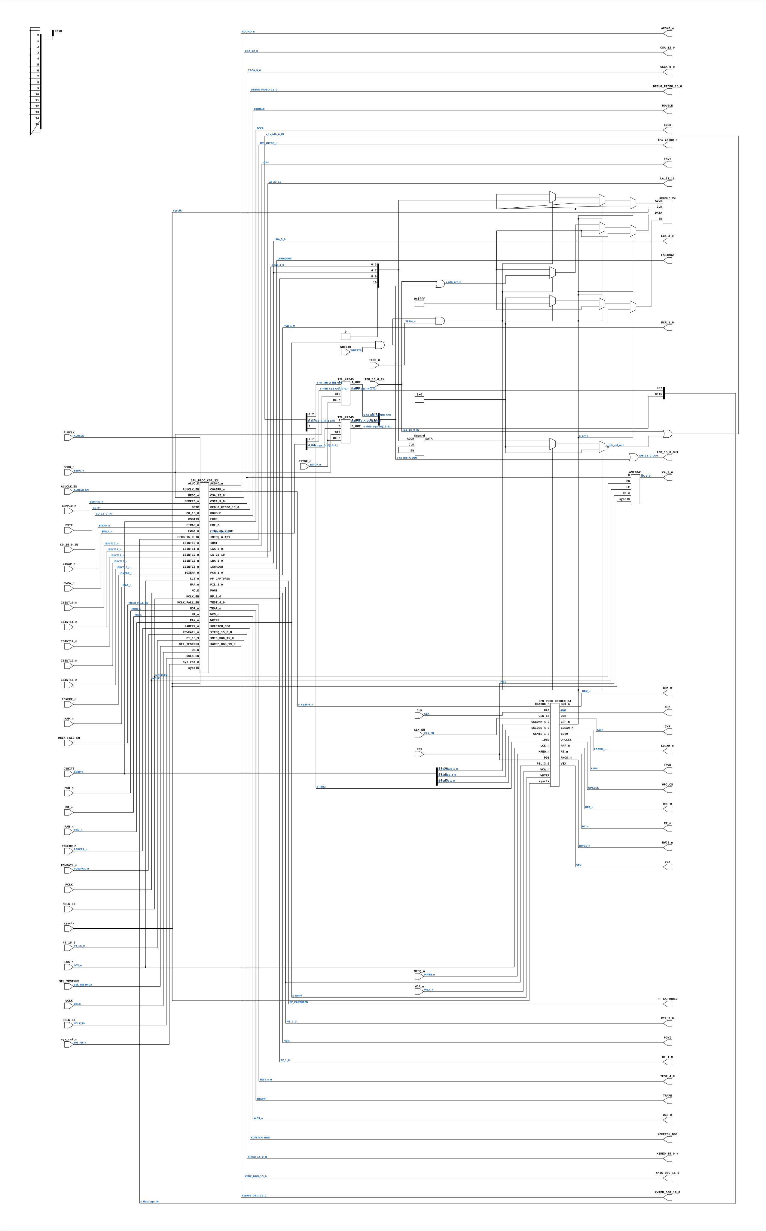
Contains: AM29841, CPU_PROC_CGA_33, CPU_PROC_CMDDEC_34, TTL_74245 x2
Module hierarchy - All modules
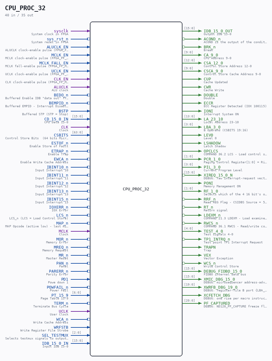
Schematic
Drawn from the Verilog: the yosys netlist of the Simulation (Verilator) build, instance CORE.CPU_BOARD.CPU.PROC. Sub-modules are boxes (click the picture to open it full size; there every sub-module box links to its page, and every wire shows its Verilog name).
Description
ND120 CPU, MM&M CPU/PROC PROCESSOR TOP LEVEL SHEET 32 of 50 Last reviewed: 2-FEB-2025 Ronny Hansen
Ports
| Direction | Width | Name | Description |
|---|---|---|---|
| input | 1 |
sysclk |
System clock in FPGA |
| input | 1 |
sys_rst_n (active low) |
System reset in FPGA |
| input | 1 |
ALUCLK_EN |
ALUCLK clock-enable pulse (FPGA_FF_MODE, else 0) |
| input | 1 |
MCLK_EN |
MCLK clock-enable pulse (FPGA_FF_MODE, else 0) |
| input | 1 |
MCLK_FALL_EN |
MCLK fall-enable pulse (FPGA_FF_MODE, else 0) |
| input | 1 |
UCLK_EN |
UCLK clock-enable pulse (FPGA_FF_MODE, else 0) |
| input | 1 |
CLK_EN |
CLK clock-enable pulse (FPGA_FF_MODE, else 0) |
| input | 1 |
ALUCLK |
ALU clock |
| input | 1 |
BEDO_n (active low) |
Buffered Enable IDB "data out" from CGA |
| input | 1 |
BEMPID_n (active low) |
Buffered EMPID - Interrupt Disable (EPIC.LDMPIE->set mask reg:inh all ints) |
| input | 1 |
BSTP |
Buffered STP (STP = Stop) |
| input | [15:0] |
CD_15_0_IN |
CPU Data 15-0 |
| input | 1 |
CLK |
Clock |
| input | [63:0] |
CSBITS |
Control Store Bits (64 bits Microcode) |
| input | 1 |
ESTOF_n (active low) |
Enable Store of Fault |
| input | 1 |
ETRAP_n (active low) |
Enable Trap |
| input | 1 |
EWCA_n (active low) |
Enable Write Cache Address |
| input | 1 |
IBINT10_n (active low) |
Input Interrupt 10 |
| input | 1 |
IBINT11_n (active low) |
Input Interrupt 11 |
| input | 1 |
IBINT12_n (active low) |
Input Interrupt 12 |
| input | 1 |
IBINT13_n (active low) |
Input Interrupt 13 |
| input | 1 |
IBINT15_n (active low) |
Input Interrupt 15 |
| input | 1 |
IOXERR_n (active low) |
IOX Error |
| input | 1 |
LCS_n (active low) |
LCS_n (LCS = Load Control Store) |
| input | 1 |
MAP_n (active low) |
MAP Opcode (active low) - last microinstruction of every macro instruction |
| input | 1 |
MCLK |
Clock |
| input | 1 |
MOR_n (active low) |
Memory Error |
| input | 1 |
MREQ_n (active low) |
Memory Request |
| input | 1 |
MR_n (active low) |
Master Reset |
| input | 1 |
PAN_n (active low) |
Panel |
| input | 1 |
PARERR_n (active low) |
Parity Error |
| input | 1 |
PD1 |
Powe down 1 |
| input | 1 |
POWFAIL_n (active low) |
Power Fail |
| input | [6:0] |
PT_15_9 |
Page Table 15-9 |
| input | 1 |
TERM_n (active low) |
Terminate Bus Cycle |
| input | 1 |
UCLK |
User Clock |
| input | 1 |
WCA_n (active low) |
Write Cache Address |
| input | 1 |
WRFSTB |
Write Register File Strobe |
| input | [2:0] |
SEL_TESTMUX |
Selects testmux signals to output on TEST_4_0 |
| input | [15:0] |
IDB_15_0_IN |
Input IDB 15-0 |
| output | [15:0] |
IDB_15_0_OUT |
Output IDB 15-0 |
| output | 1 |
ACOND_n (active low) |
ACOND is the output of the condition register. |
| output | 1 |
BRK_n (active low) |
Break |
| output | [9:0] |
CA_9_0 |
CPU Address 9-0 |
| output | [12:0] |
CSA_12_0 |
Control Store Address 12-0 |
| output | [9:0] |
CSCA_9_0 |
Control Store Cache Address 9-0 |
| output | 1 |
CUP |
Cache Updated |
| output | 1 |
CWR |
Cache Write |
| output | 1 |
DOUBLE |
Double |
| output | 1 |
ECCR |
ECC Register Detected (IOX 100115) |
| output | 1 |
IONI |
Interrupt System ON |
| output | [13:0] |
LA_23_10 |
Local Address 23-10 |
| output | [3:0] |
LBA_3_0 |
B Operand (CSBITS 19:16) |
| output | 1 |
LEV0 |
Level 0 |
| output | 1 |
LSHADOW |
Latch Shadow |
| output | 1 |
OPCLCS |
COMMAND 36.2 LCS - Load control store from PROM and perform a Master Clear |
| output | [1:0] |
PCR_1_0 |
Paging Control Register[1:0] = Ring Protection Level |
| output | [3:0] |
PIL_3_0 |
Current Program Level |
| output | [15:0] |
XIREQ_15_0_N (active low) |
DEBUG: raw interrupt-request vector (active low) |
| output | 1 |
PONI |
Memory Management ON |
| output | [1:0] |
RF_1_0 |
Selects which of the 4 16 bit's of the microcode to fetch from ROM |
| output | 1 |
RRF_n (active low) |
Read REG Flag - CSIDBS Source = 5 (REG) |
| output | 1 |
RT_n (active low) |
Return signal |
| output | 1 |
LDEXM_n (active low) |
COMMAND 21.3 LDEXM - Load examine mode in MAC function |
| output | 1 |
RWCS_n (active low) |
COMMAND 36.1 RWCS - Read/write control store as addressed by ADCS command |
| output | [4:0] |
TEST_4_0 |
Test signals 4-0 |
| output | 1 |
TP1_INTRQ_n (active low) |
Test point TP1 Interrupt Request |
| output | 1 |
TRAPN |
Trap |
| output | 1 |
VEX |
Vector Exception |
| output | 1 |
WCS_n (active low) |
Write Control Store |
| output | [15:0] |
DEBUG_FIDBO_15_0 |
FIDBO internal data bus |
| output | [15:0] |
XMIC_DBG_15_0 |
DEBUG: microsequencer address-advance probe (Tang 06000-hang) |
| output | [19:0] |
XWRFB_DBG_19_0 |
DEBUG: register-file B port {LBA_3_0, B_15_0} - STERR error number |
| output | 1 |
XCFETCH_DBG |
DEBUG: one rise per macro instruction (see CGA.v) |
| output | [20:0] |
PF_CAPTURED |
DEBUG: ND120_PF_CAPTURE freeze flag (23-AUG) |
Verilog source
Verilog/CPU-BOARD-3202/circuit/CPU_PROC_32.v on GitHub.
Show the Verilog of CPU_PROC_32 (573 lines)
/**************************************************************************
** ND120 CPU, MM&M **
** CPU/PROC **
** PROCESSOR TOP LEVEL **
** SHEET 32 of 50 **
** **
** Last reviewed: 2-FEB-2025 **
** Ronny Hansen **
***************************************************************************/
module CPU_PROC_32 (
input sysclk, // System clock in FPGA
input sys_rst_n, // System reset in FPGA
input ALUCLK_EN, //! ALUCLK clock-enable pulse (FPGA_FF_MODE, else 0)
input MCLK_EN, //! MCLK clock-enable pulse (FPGA_FF_MODE, else 0)
input MCLK_FALL_EN, //! MCLK fall-enable pulse (FPGA_FF_MODE, else 0)
input UCLK_EN, //! UCLK clock-enable pulse (FPGA_FF_MODE, else 0)
input CLK_EN, //! CLK clock-enable pulse (FPGA_FF_MODE, else 0)
input ALUCLK, //! ALU clock
input BEDO_n, //! Buffered Enable IDB "data out" from CGA
input BEMPID_n, //! Buffered EMPID - Interrupt Disable (EPIC.LDMPIE->set mask reg:inh all ints)
input BSTP, //! Buffered STP (STP = Stop)
input [15:0] CD_15_0_IN, //! CPU Data 15-0
input CLK, //! Clock
input [63:0] CSBITS, //! Control Store Bits (64 bits Microcode)
input ESTOF_n, //! Enable Store of Fault
input ETRAP_n, //! Enable Trap
input EWCA_n, //! Enable Write Cache Address
input IBINT10_n, //! Input Interrupt 10
input IBINT11_n, //! Input Interrupt 11
input IBINT12_n, //! Input Interrupt 12
input IBINT13_n, //! Input Interrupt 13
input IBINT15_n, //! Input Interrupt 15
input IOXERR_n, //! IOX Error
input LCS_n, //! LCS_n (LCS = Load Control Store)
input MAP_n, //! MAP Opcode (active low) - last microinstruction of every macro instruction
input MCLK, //! Clock
input MOR_n, //! Memory Error
input MREQ_n, //! Memory Request
input MR_n, //! Master Reset
input PAN_n, //! Panel
input PARERR_n, //! Parity Error
input PD1, //! Powe down 1
input POWFAIL_n, //! Power Fail
input [ 6:0] PT_15_9, //! Page Table 15-9
input TERM_n, //! Terminate Bus Cycle
input UCLK, //! User Clock
input WCA_n, //! Write Cache Address
input WRFSTB, //! Write Register File Strobe
input [ 2:0] SEL_TESTMUX, //! Selects testmux signals to output on TEST_4_0
/*******************************************************************************
** The IN and OUT are define here **
*******************************************************************************/
input [15:0] IDB_15_0_IN, //! Input IDB 15-0
output [15:0] IDB_15_0_OUT, //! Output IDB 15-0
/*******************************************************************************
** The outputs are defined here **
*******************************************************************************/
output ACOND_n, //! ACOND is the output of the condition register.
output BRK_n, //! Break
output [ 9:0] CA_9_0, //! CPU Address 9-0
output [12:0] CSA_12_0, //! Control Store Address 12-0
output [ 9:0] CSCA_9_0, //! Control Store Cache Address 9-0
output CUP, //! Cache Updated
output CWR, //! Cache Write
output DOUBLE, //! Double
output ECCR, //! ECC Register Detected (IOX 100115)
output IONI, //! Interrupt System ON
output [13:0] LA_23_10, //! Local Address 23-10
output [ 3:0] LBA_3_0, //! B Operand (CSBITS 19:16)
output LEV0, //! Level 0
output LSHADOW, //! Latch Shadow
output OPCLCS, //! COMMAND 36.2 LCS - Load control store from PROM and perform a Master Clear
output [ 1:0] PCR_1_0, //! Paging Control Register[1:0] = Ring Protection Level
output [ 3:0] PIL_3_0, //! Current Program Level
output [15:0] XIREQ_15_0_N, //! DEBUG: raw interrupt-request vector (active low)
output PONI, //! Memory Management ON
output [ 1:0] RF_1_0, //! Selects which of the 4 16 bit's of the microcode to fetch from ROM
output RRF_n, //! Read REG Flag - CSIDBS Source = 5 (REG)
output RT_n, //! Return signal
output LDEXM_n, //! COMMAND 21.3 LDEXM - Load examine mode in MAC function
output RWCS_n, //! COMMAND 36.1 RWCS - Read/write control store as addressed by ADCS command
output [ 4:0] TEST_4_0, //! Test signals 4-0
output TP1_INTRQ_n, //! Test point TP1 Interrupt Request
output TRAPN, //! Trap
output VEX, //! Vector Exception
output WCS_n, //! Write Control Store
// Debug
output [15:0] DEBUG_FIDBO_15_0, //! FIDBO internal data bus
output [15:0] XMIC_DBG_15_0, //! DEBUG: microsequencer address-advance probe (Tang 06000-hang)
output [19:0] XWRFB_DBG_19_0, //! DEBUG: register-file B port {LBA_3_0, B_15_0} - STERR error number
output XCFETCH_DBG, //! DEBUG: one rise per macro instruction (see CGA.v)
output [20:0] PF_CAPTURED //! DEBUG: ND120_PF_CAPTURE freeze flag (23-AUG)
);
/*******************************************************************************
** The wires are defined here **
*******************************************************************************/
wire [63:0] s_csbits;
wire [15:0] s_fidb_cga_IN; // Out from B side of CHIP32 and 33, and IN to CGA
wire [15:0] s_fidb_cga_OUT; // Input signal to B side of CHIP32 and 33, and OUT from CGA
wire [15:0] s_tx_idb_A_IN; // Input signal to A side of CHIP32 and 33 (transcievers)
wire [15:0] s_tx_idb_A_OUT; // Out from A side of CHIP32 and 33 (transcievers)
wire [15:0] s_tx_idb_B_IN; // Input signal to B side of CHIP32 and 33 (transcievers)
wire [15:0] s_tx_idb_B_OUT; // Out from B side of CHIP32 and 33 (transcievers)
wire [15:0] s_idb_erf_in; // 16 bit-input signal from RAM Chip34 and 35, controlled by ERF_n
wire [15:0] s_idb_erf_out; // 16 bit-output signal from RAM Chip34 and 35, controlled by ERF_n
wire [ 1:0] s_csmis_1_0;
wire [ 1:0] s_pcr_1_0;
wire [ 1:0] s_rf_1_0;
wire [10:0] s_address_10_0;
wire [12:0] s_csa_12_0;
wire [13:0] s_la_23_10;
wire [15:0] s_cd_15_0_in;
wire [ 3:0] s_laa_3_0;
wire [ 3:0] s_lba_3_0;
wire [ 3:0] s_pil_3_0;
wire [ 4:0] s_cscomm_4_0;
wire [ 4:0] s_csidbs_4_0;
wire [ 4:0] s_test_4_0;
wire [ 6:0] s_pt_15_9;
wire [ 9:0] s_ca_9_0;
wire [ 9:0] s_csca_9_0;
wire s_idb2; //IDB2 input signal to CMDDEC
wire s_acond_n;
wire s_aluclk;
wire s_bedo_n;
wire s_bempid_n;
wire s_brk_n;
wire s_bstp;
wire s_cgabrk_n;
wire s_clk;
wire s_cup;
wire s_cwr;
wire s_double;
wire s_eccr;
wire s_erf_n; // New signal, includ PAL fix to enable when CSIDBS = 5, REG (Read Register File)
wire s_estof_n;
wire s_etrap_n;
wire s_ewca_n;
wire s_ibint10_n;
wire s_ibint11_n;
wire s_ibint12_n;
wire s_ibint13_n;
wire s_ibint15_n;
wire s_ioni;
wire s_ioxerr_n;
wire s_lcs_n;
wire s_ledexm;
wire s_lev0;
wire s_lshadow;
wire s_map_n;
wire s_mclk;
wire s_mor_n;
wire s_mr_n;
wire s_mreq_n;
wire s_opclcs;
wire s_pan_n;
wire s_parerr_n;
wire s_pd1;
wire s_poni;
wire s_powfail_n;
wire s_rrf_n;
wire s_rt_n;
wire s_rwcs_n;
wire s_term_n;
wire s_tp1_intrq_n;
wire s_trap_n_out;
wire s_twrf_n;
wire s_uclk;
wire s_vex;
wire s_wca_n;
wire s_wcs_n;
wire s_wrfstb;
wire s_wrtrf;
/*******************************************************************************
** The module functionality is described here **
*******************************************************************************/
/*******************************************************************************
** Here all wiring is defined **
*******************************************************************************/
assign s_cscomm_4_0[4:0] = s_csbits[36:32];
assign s_csidbs_4_0[4:0] = s_csbits[41:37];
assign s_csmis_1_0[1:0] = s_csbits[43:42];
/*******************************************************************************
** Here all input connections are defined **
*******************************************************************************/
assign s_csbits[63:0] = CSBITS;
assign s_pt_15_9[6:0] = PT_15_9;
assign s_cd_15_0_in[15:0] = CD_15_0_IN;
assign s_ibint11_n = IBINT11_n;
assign s_uclk = UCLK;
assign s_ioxerr_n = IOXERR_n;
assign s_etrap_n = ETRAP_n;
assign s_aluclk = ALUCLK;
wire s_aluclk_en;
assign s_aluclk_en = ALUCLK_EN;
wire s_mclk_en;
assign s_mclk_en = MCLK_EN;
wire s_mclk_fall_en;
assign s_mclk_fall_en = MCLK_FALL_EN;
wire s_uclk_en;
assign s_uclk_en = UCLK_EN;
wire s_clk_en;
assign s_clk_en = CLK_EN;
assign s_map_n = MAP_n;
assign s_ibint13_n = IBINT13_n;
assign s_ibint10_n = IBINT10_n;
assign s_bempid_n = BEMPID_n;
assign s_bstp = BSTP;
assign s_ibint15_n = IBINT15_n;
assign s_lcs_n = LCS_n;
assign s_mclk = MCLK;
assign s_powfail_n = POWFAIL_n;
assign s_parerr_n = PARERR_n;
assign s_wrfstb = WRFSTB;
assign s_pan_n = PAN_n;
assign s_bedo_n = BEDO_n;
assign s_pd1 = PD1;
assign s_mreq_n = MREQ_n;
assign s_term_n = TERM_n;
assign s_clk = CLK;
assign s_mr_n = MR_n;
assign s_ewca_n = EWCA_n;
assign s_ibint12_n = IBINT12_n;
assign s_mor_n = MOR_n;
assign s_estof_n = ESTOF_n;
assign s_wca_n = WCA_n;
// s_twrf_n = low, write to memory from IDB
/*
REMOVED, making it easy with OR only
wire ram_read; // boolean to know if we are reading from RAM
assign ram_read = !s_erf_n & s_wrtrf & s_twrf_n; // Read from RAM
assign s_fidb_A_IN = IDB_15_0_IN | (ram_read) ? s_idb_erf_out : 0;
assign s_fidb_cga_IN = s_fidb_B_OUT;
assign s_idb2 = s_fidb_A_IN[2];
// Not 100% sure where data to the RAM may come from, so expect it to com from IDB and via Chip32F/33F
assign s_idb_erf_in = IDB_15_0_IN | ((!ESTOF_n & !BEDO_n) ? s_fidb_A_OUT : 0);
// use LOGIC to select
assign IDB_15_0_OUT = ram_read ? s_idb_erf_out[15:0] : ( (!ESTOF_n & !BEDO_n) ? s_fidb_A_OUT[15:0] : 16'b0);
// use OR to combine singals
//assign IDB_15_0_OUT = s_idb_erf_inout[15:0] | s_fidb_A_OUT[15:0];
*/
// Connect CGA IDB with CHIP32/33 IDB
assign s_tx_idb_B_IN = s_fidb_cga_OUT;
assign s_fidb_cga_IN = s_tx_idb_B_OUT;
// Connect incomming IDB signal to Transciever and RAM chips
assign s_tx_idb_A_IN = IDB_15_0_IN | s_idb_erf_out;
assign IDB_15_0_OUT = s_idb_erf_out[15:0] | s_tx_idb_A_OUT[15:0];
assign s_idb_erf_in = IDB_15_0_IN | s_tx_idb_A_OUT;
assign s_idb2 = s_tx_idb_A_IN[2];
assign s_address_10_0[10] = 1'b0; // Ground
assign s_address_10_0[9:8] = s_rf_1_0[1:0];
assign s_address_10_0[7:4] = s_lba_3_0[3:0];
assign s_address_10_0[3:0] = s_laa_3_0[3:0];
assign s_twrf_n = ~(s_wrtrf & s_wrfstb & s_term_n);
/*******************************************************************************
** Here all output connections are defined **
*******************************************************************************/
assign ACOND_n = s_acond_n;
assign BRK_n = s_brk_n;
assign CA_9_0 = s_ca_9_0[9:0];
assign CSA_12_0 = s_csa_12_0[12:0];
assign CSCA_9_0 = s_csca_9_0[9:0];
assign CUP = s_cup;
assign CWR = s_cwr;
assign DOUBLE = s_double;
assign ECCR = s_eccr;
assign IONI = s_ioni;
assign LA_23_10 = s_la_23_10[13:0];
assign LBA_3_0 = s_lba_3_0;
assign LEV0 = s_lev0;
assign LSHADOW = s_lshadow;
assign OPCLCS = s_opclcs;
assign PCR_1_0 = s_pcr_1_0[1:0];
assign PIL_3_0 = s_pil_3_0[3:0];
assign PONI = s_poni;
assign RF_1_0 = s_rf_1_0[1:0];
assign RRF_n = s_rrf_n;
assign RT_n = s_rt_n;
assign LDEXM_n = s_ledexm;
assign RWCS_n = s_rwcs_n;
assign TEST_4_0 = s_test_4_0[4:0];
assign TP1_INTRQ_n = s_tp1_intrq_n;
assign TRAPN = s_trap_n_out;
assign VEX = s_vex;
assign WCS_n = s_wcs_n;
/*******************************************************************************
** Here all in-lined components are defined **
*******************************************************************************/
/*******************************************************************************
** Here all sub-circuits are defined **
*******************************************************************************/
// P3 (docs/plan-fix-unconstrained-clocks.md): in FF mode the CA latch
// captures on posedge sysclk gated by the rise-aligned MCLK enable
// instead of clocking on the routed s_mclk net (mclk_Z clock root).
`ifdef FPGA_FF_MODE
localparam CA_LATCH_CE = 1;
`else
localparam CA_LATCH_CE = 0;
`endif
AM29841 #(.USE_ENABLE(CA_LATCH_CE)) CHIP_25F (
.sysclk(sysclk),
.EN(s_mclk_en),
// Input signals
.D(s_csca_9_0),
.LE(s_mclk),
.OE_n(s_pd1),
// Output signals
.Y(s_ca_9_0)
);
/*
* This module, CPU_PROC_CMDDEC_34, is responsible for decoding various control signals
* within the CPU processor. It takes multiple input signals related to clock, control store,
* and memory requests, and processes them to generate a set of output signals. These outputs
* include break signals, cache update and write signals, error flags, and various control
* and status signals that are essential for the CPU's operation and management of tasks.
*/
CPU_PROC_CMDDEC_34 CMDDEC (
// Inputs
.sysclk(sysclk), // FPGA system clock
.CLK_EN(s_clk_en), // CLK clock-enable pulse (FPGA_FF_MODE)
.CGABRK_n(s_cgabrk_n), // CPU Break Signal
.CLK(s_clk), // Clock
.CSCOMM_4_0(s_cscomm_4_0[4:0]), // Control Store - Command
.CSIDBS_4_0(s_csidbs_4_0[4:0]), // Control Store - IDB Source
.CSMIS_1_0(s_csmis_1_0[1:0]), // Control Store - MIS bits
.IDB2(s_idb2), // IDB bit 2 input signal
.LCS_n(s_lcs_n), // Load Control Store
.MREQ_n(s_mreq_n), // Memory Request
.PD1(s_pd1), // Power Down 1
.WCA_n(s_wca_n), // Write Cache Address
.WRTRF(s_wrtrf), // Write Register File
// Outputs
.BRK_n(s_brk_n), // Break signal
.CUP(s_cup), // Cache Updated
.CWR(s_cwr), // Cache Write
.ERF_n(s_erf_n), // Enable RAM Flag
.LDEXM_n(s_ledexm), // Load Examine Mode
.LEV0(s_lev0), // Level 0
.OPCLCS(s_opclcs), // COMMAND 36.2 LCS - Load control store from PROM and perform a Master Clear
.PIL_3_0(s_pil_3_0[3:0]), // Current Program Level
.RRF_n(s_rrf_n), // Read Register Flag
.RT_n(s_rt_n), // Return signal
.RWCS_n(s_rwcs_n), // Read/Write Control Store
.VEX(s_vex) // Vector Exception
);
TTL_74245 CHIP_32F (
// Input signals
.DIR(s_bedo_n),
.OE_n(s_estof_n),
// Input and Output bus
.A(s_tx_idb_A_IN[7:0]),
.A_OUT(s_tx_idb_A_OUT[7:0]),
.B(s_tx_idb_B_IN[7:0]),
.B_OUT(s_tx_idb_B_OUT[7:0])
);
TTL_74245 CHIP_33F (
// Input signals
.DIR(s_bedo_n),
.OE_n(s_estof_n),
// Input and Output bus signals
.A(s_tx_idb_A_IN[15:8]),
.A_OUT(s_tx_idb_A_OUT[15:8]),
.B(s_tx_idb_B_IN[15:8]),
.B_OUT(s_tx_idb_B_OUT[15:8])
);
/*
TMM2018D_25 CHIP_34F (
.clk(sysclk), // System clock in FPGA
.reset_n(sys_rst_n), // System reset in FPGA
.ADDRESS(s_address_10_0[10:0]),
.CS_n (s_erf_n),
.D (s_idb_erf_in[7:0]), // IN
.D_OUT (s_idb_erf_out[7:0]), // OUT
.OE_n (s_wrtrf),
.W_n (s_twrf_n)
);
TMM2018D_25 CHIP_35F (
.clk(sysclk), // System clock in FPGA
.reset_n(sys_rst_n), // System reset in FPGA
.ADDRESS(s_address_10_0[10:0]),
.CS_n (s_erf_n),
.D (s_idb_erf_in[15:8]), // IN
.D_OUT (s_idb_erf_out[15:8]), // OUT
.OE_n (s_wrtrf),
.W_n (s_twrf_n)
);
*/
//2x RAM 2^11 addresses, Each 8-bit wide. Converted to one 16 bits wide
// yosys: the asynchronous read on s_idb_erf_out (assign below) cannot map
// to a BSRAM, and yosys treats ram_style="block" as a hard requirement
// ("ERROR: no valid mapping") where Vivado/Gowin EDA treat it as advisory
// and fall back. 2048x16 = 32 Kbit as distributed LUT RAM (~2K LUT4).
// yosys pre-defines YOSYS; every other flow is untouched.
// QUARTUS (MiSTer, Cyclone V): this array builds as written. An explicit
// altsyncram (MLAB, UNREGISTERED) arm was added 31-AUG-2026 when Quartus
// refused the plain array - but it refused only because the WCS was failing
// at the same time and their COMBINED register-fallback demand overflowed
// the device. With the WCS in real M10K (QUARTUS_RAM_INFER), this array
// alone is ~32,768 FFs (about 16K ALMs against 41,910) and build v47
// (01-SEP-2026) built and booted it exactly as the RTL below describes.
// The megafunction arm was deleted the same day: this is the CPU REGISTER
// FILE, read by every instruction, and its combinational read was only ever
// verified against a hand-written altsyncram stub in simulation - never
// against real Quartus MLAB silicon. Letting Quartus build what the RTL
// says takes that unverified assumption out of the CPU's most critical
// path, and it is the same reason the WCS and main-memory megafunction
// arms went (see Shared/support/IDT6168A_20.v).
`ifdef YOSYS
(* ram_style = "distributed" *) reg [15:0] registerBlock[0:2047];
`else
(* ram_style = "block" *) reg [15:0] registerBlock[0:2047];
`endif
always @(posedge sysclk) // or negedge s_twrf_n)
begin
if (!s_erf_n) begin
if (!s_twrf_n) begin
// Write operation: active when chip is selected and write enable is low
registerBlock[s_address_10_0[10:0]] <= s_idb_erf_in;
end
end
end
// s_erf_n <= CHIP SELECT active low (Enable Register File negated)
// s_twrf_n = 0 <== WRITE TO registerBlock. s_twrf_n == 1, READ FROM registerBlock
assign s_idb_erf_out = s_erf_n ? 16'b0 : s_twrf_n ? registerBlock[s_address_10_0[10:0]] : 16'b0;
/*
* The CGA (CPU Gate Array) module is the core of the CPU. It handles the control
* and interrupt processing. It manages the cache address generation, memory
* protection levels, program interrupt levels, and various control signals
* for the CPU. It interfaces with the ALU, memory subsystem, and interrupt
* handling logic.
*/
CPU_PROC_CGA_33 CGA (
// System signals
.sysclk (sysclk), // input
.sys_rst_n(sys_rst_n), // input
// Inputs
.ALUCLK_EN(s_aluclk_en), // ALUCLK clock-enable pulse
.MCLK_EN(s_mclk_en), // MCLK clock-enable pulse
.MCLK_FALL_EN(s_mclk_fall_en), // MCLK fall-enable pulse
.UCLK_EN(s_uclk_en), // UCLK clock-enable pulse
.ALUCLK(s_aluclk), // ALU clock signal
.BEDO_n(s_bedo_n), // Buffered Enable IDB "data out" from CGA
.BEMPID_n(s_bempid_n), // Buffered EMPID - Interrupt Disable (EPIC.LDMPIE->set mask reg:inh all ints)
.BSTP(s_bstp), // Buffered Stop signal
.CD_15_0(s_cd_15_0_in[15:0]), // CPU Data bus 15-0
.CSBITS(s_csbits[63:0]), // Control Store Bits for microcode
.ETRAP_n(s_etrap_n), // Enable Trap signal
.EWCA_n(s_ewca_n), // Enable Write Cache Address
.FIDB_15_0_IN(s_fidb_cga_IN[15:0]), // Input to B side of CHIP32 and 33
.IBINT10_n(s_ibint10_n), // Input Bus Interrupt 10
.IBINT11_n(s_ibint11_n), // Input Bus Interrupt 11
.IBINT12_n(s_ibint12_n), // Input Bus Interrupt 12
.IBINT13_n(s_ibint13_n), // Input Bus Interrupt 13
.IBINT15_n(s_ibint15_n), // Input Bus Interrupt 15
.IOXERR_n(s_ioxerr_n), // IOX Error signal
.LCS_n(s_lcs_n), // Load Control Store signal
.MAP_n(s_map_n), // MAP Opcode (active low)
.MCLK(s_mclk), // Microcycle clock
.MOR_n(s_mor_n), // Memory Error signal
.MR_n(s_mr_n), // Master Reset signal
.PAN_n(s_pan_n), // Panel signal
.PARERR_n(s_parerr_n), // Parity Error signal
.POWFAIL_n(s_powfail_n), // Power Fail signal
.PT_15_9(s_pt_15_9[6:0]), // Page Table bits 15:9
.SEL_TESTMUX(SEL_TESTMUX), // Selects testmux signals
.UCLK(s_uclk), // User Clock signal
// Outputs
.ACOND_n(s_acond_n), // ACOND signal
.CGABRK_n(s_cgabrk_n), // CGA Break signal
.CSA_12_0(s_csa_12_0[12:0]), // Control Store Address 12-0
.CSCA_9_0(s_csca_9_0[9:0]), // Control Store Cache Address 9-0
.DOUBLE(s_double), // Double signal
.ECCR(s_eccr), // ECC Register Detected
.ERF_n(), // Enable Register File original signal fromn CGA (Original signal from CGA. Not used after fix has been applied)
.FIDB_15_0_OUT(s_fidb_cga_OUT[15:0]), // Output from B side of CHIP32 and 33
.INTRQ_n_tp1(s_tp1_intrq_n), // Interrupt Request Test Point 1
.IONI(s_ioni), // Interrupt System ON
.LAA_3_0(s_laa_3_0[3:0]), // A Operand
.LBA_3_0(s_lba_3_0[3:0]), // B Operand
.LA_23_10(s_la_23_10[13:0]), // Local Address - bits 23-10
.LSHADOW(s_lshadow), // Latch Shadow Memory signal
.PCR_1_0(s_pcr_1_0[1:0]), // Paging Control Register 1-0
.PIL_3_0(s_pil_3_0[3:0]), // Current Program Level
.XIREQ_15_0_N(XIREQ_15_0_N), // DEBUG: raw interrupt-request vector
.PONI(s_poni), // Memory Management ON
.RF_1_0(s_rf_1_0), // Selects microcode from ROM
.TEST_4_0(s_test_4_0[4:0]), // Test signals 4-0
.TRAP_n(s_trap_n_out), // Trap signal
.WCS_n(s_wcs_n), // Write Control Store
.WRTRF(s_wrtrf), // Write Register File Strobe
.DEBUG_FIDBO_15_0(DEBUG_FIDBO_15_0),
.XMIC_DBG_15_0(XMIC_DBG_15_0),
.XWRFB_DBG_19_0(XWRFB_DBG_19_0),
.XCFETCH_DBG(XCFETCH_DBG),
.PF_CAPTURED(PF_CAPTURED)
);
endmodule