CPU_MMU_PPNX_28
Source: Verilog/CPU-BOARD-3202/circuit/CPU_MMU_PPNX_28.v
Where it sits (Simulation): ND120_TOP > ND120_CORE > ND3202D > CPU_15 > CPU_MMU_24 > CPU_MMU_PPNX_28
- instance path: CORE.CPU_BOARD.CPU.MMU.PPNX
Used in: CPU_MMU_24 (all tops)
Contains: no other modules.
Module hierarchy - All modules
Schematic
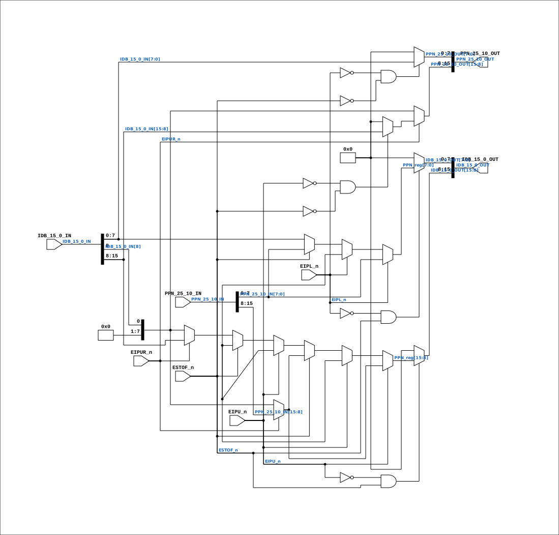
Drawn from the Verilog: the yosys netlist of the Simulation (Verilator) build, instance CORE.CPU_BOARD.CPU.MMU.PPNX. Sub-modules are boxes (click the picture to open it full size; there every sub-module box links to its page, and every wire shows its Verilog name).
Description
ND120 CPU, MM&M CPU/MMU/PPNX PPN TO IDB SHEET 28 of 50 Last reviewed: 2-FEB-2025 Ronny Hansen
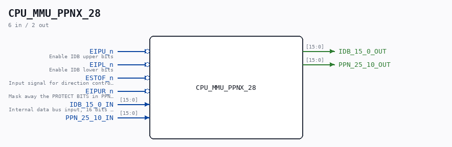
Ports
| Direction | Width | Name | Description |
|---|---|---|---|
| input | 1 |
EIPU_n (active low) |
Enable IDB upper bits |
| input | 1 |
EIPL_n (active low) |
Enable IDB lower bits |
| input | 1 |
ESTOF_n (active low) |
Input signal for direction control (PPN<->IDB) |
| input | 1 |
EIPUR_n (active low) |
Mask away the PROTECT BITS in PPN (PPN 25:19 == 000000) |
| input | [15:0] |
IDB_15_0_IN |
Internal data bus input, 16 bits (from CPU_MMU_24.IDB_15_0_IN) |
| output | [15:0] |
IDB_15_0_OUT |
|
| input | [15:0] |
PPN_25_10_IN |
|
| output | [15:0] |
PPN_25_10_OUT |
Verilog source
Verilog/CPU-BOARD-3202/circuit/CPU_MMU_PPNX_28.v on GitHub.
Show the Verilog of CPU_MMU_PPNX_28 (139 lines)
/**************************************************************************
** ND120 CPU, MM&M                                                       **
** CPU/MMU/PPNX                                                          **
** PPN TO IDB                                                            **
** SHEET 28 of 50                                                        **
**                                                                       **
** Last reviewed: 2-FEB-2025                                            **
** Ronny Hansen                                                          **
***************************************************************************/

module CPU_MMU_PPNX_28 (
  input EIPU_n,   //! Enable IDB upper bits
  input EIPL_n,   //! Enable IDB lower bits
  input ESTOF_n,  //! Input signal for direction control (PPN<->IDB)

  input EIPUR_n,  //! Mask away the PROTECT BITS in PPN (PPN 25:19 == 000000)

  input  [15:0] IDB_15_0_IN,  //! Internal data bus input, 16 bits (from CPU_MMU_24.IDB_15_0_IN)
  output [15:0] IDB_15_0_OUT,

  input  [15:0] PPN_25_10_IN,
  output [15:0] PPN_25_10_OUT
);


  wire DIR = ESTOF_n;

  reg [15:0] PPN_reg;
  reg [15:0] IDB_reg;

  always @(*)
  begin
    IDB_reg = IDB_15_0_IN;
    PPN_reg = PPN_25_10_IN;

    if (EIPUR_n == 0) begin
      PPN_reg[15:8] = {7'b0, IDB_15_0_IN[8]};
      PPN_reg[7:0]  = PPN_25_10_IN[7:0];
    end


    // 2x 74245 (CHIP 10B (UPPER) and 9B (LOWER))
    //always @(*) begin


    // Upper 8 bits - CHIP 10B
    if (EIPU_n == 0) begin
      if (DIR) begin
        // Data flows from A to B
        IDB_reg[15:8] = PPN_reg[15:8];
      end else begin
        // Data flows from B to A

        if (EIPUR_n == 0) begin
          PPN_reg[15:8] = {7'b0, IDB_15_0_IN[8]};
        end else begin
          PPN_reg[15:8] = IDB_15_0_IN[15:8];
        end
      end
      /*end else begin
       PPN_reg[15:8] = PPN_25_10[15:8];
       IDB_reg[15:8] = IDB_15_0[15:8];
   */
    end

    // Lower 8 bits - CHIP 9B
    if (EIPL_n == 0) begin
      if (DIR) begin
        IDB_reg[7:0] = PPN_reg[7:0];  // Data flows from A to B
      end else begin
        PPN_reg[7:0] = IDB_15_0_IN[7:0];  // Data flows from B to A
      end
      /*
   end else begin
       PPN_reg[7:0] = PPN_25_10[7:0];
       IDB_reg[7:0] = IDB_15_0[7:0];
   */
    end
  end

  // Assign the bidirectional bus with respect to OE.
  //
  // Sheet 28 of the 3202D drawing has three chips: 10B (74PCT245, IDB15-8 <->
  // PPN25-18, /G = EIPU_n), 9B (74PCT245, IDB7-0 <-> PPN17-10, /G = EIPL_n)
  // and 8B (74LS244, /G = EIPUR_n, PPN25-19 grounded and PPN18 = IDB8). DIR
  // is shared and comes from ESTOF_n: 1 = A to B = PPN to IDB.
  //
  // Both output assignments used to publish the working registers with NO
  // enable term, and those registers are seeded from this module's own
  // inputs - so a disabled byte, or the opposite direction, echoed the input
  // straight back out. That put PPN_25_10_IN permanently on PPN_25_10_OUT and
  // IDB_15_0_IN permanently on IDB_15_0_OUT, which the parents merge with a
  // wired-OR, feeding the CGA its own IDB output back into its IDB input
  // (CPU_15.v:331 -> here -> CPU_15.v:336) and the shadow RAM its own read
  // data back into its write data (CPU_MMU_24.v:221 -> here -> :220).
  // The sibling sheet 30 (CPU_MMU_PTIDB_30.v:46-49) always gated its pair
  // correctly, as does the reference model Shared/support/TTL_74245.v:25-28.
  // A disabled driver puts 0 on the bus - inside the FPGA there is no z.
  //
  // PPN_reg stays as the internal A-side node: the DIR=1 branches above read
  // it to forward the masked or raw PPN byte onto IDB.
  //
  // 20-AUG-2026: publish the SELECTED SOURCE, not the working register.
  // IDB_reg is seeded with IDB_15_0_IN and only overwritten from PPN_reg in
  // the (!EIPU_n && DIR) branch - so functionally the seed was never
  // published. Structurally, though, synthesis cannot prove that, and saw an
  // unconditional edge IDB_15_0_IN -> IDB_reg -> IDB_15_0_OUT. Through the
  // parents' wired-OR (CPU_15.v:331 -> here -> CPU_15.v:336) that edge closed
  // a combinational loop, and Vivado's DRC (LUTLP-1) blocks bitstream
  // generation on it. Same shape as the shared 'internalBus' node removed
  // from Shared/support/TTL_74245.v on the same day.
  //
  // PPN_reg[15:8] is exactly what IDB_reg[15:8] held whenever this output is
  // enabled, so this is the same value with no shared node.
  assign IDB_15_0_OUT[15:8]  = (!EIPU_n && DIR) ? PPN_reg[15:8] : 8'b0;
  assign IDB_15_0_OUT[7:0]   = (!EIPL_n && DIR) ? PPN_reg[7:0]  : 8'b0;

  // PPN is driven by 10B/9B in the B-to-A direction, and by 8B whenever
  // EIPUR_n is low, independently of the two transceivers. Where 8B and 10B
  // both drive the high byte the mask wins, which is what the code above
  // already resolves.
  // Same treatment on the PPN side: PPN_reg is seeded with PPN_25_10_IN, and
  // in every case where these outputs are enabled it has been overwritten
  // from the IDB side (or from the 8B mask). Naming the source directly
  // removes the PPN_25_10_IN -> PPN_reg -> PPN_25_10_OUT edge.
  //   8B (EIPUR_n) forces PPN18 = IDB8 with PPN25-19 grounded, and wins over
  //   10B where both drive - which is the priority the always block above
  //   already resolves.
  assign PPN_25_10_OUT[15:8] = !EIPUR_n            ? {7'b0, IDB_15_0_IN[8]}
                             : (!EIPU_n && !DIR)   ? IDB_15_0_IN[15:8]
                                                   : 8'b0;
  assign PPN_25_10_OUT[7:0]  = (!EIPL_n && !DIR)   ? IDB_15_0_IN[7:0] : 8'b0;


  // Output to A when receiving from B with respect to OE (OE_n==1 means "isolated". Don't write to A or B)
  //assign A = (OE_n == 0 && DIR == 0) ? internalBus : 8'b0;


endmodule