CPU_CS_16
Source: Verilog/CPU-BOARD-3202/circuit/CPU_CS_16.v
Where it sits (Simulation): ND120_TOP > ND120_CORE > ND3202D > CPU_15 > CPU_CS_16
- instance path: CORE.CPU_BOARD.CPU.CS
Used in: CPU_15 (all tops)
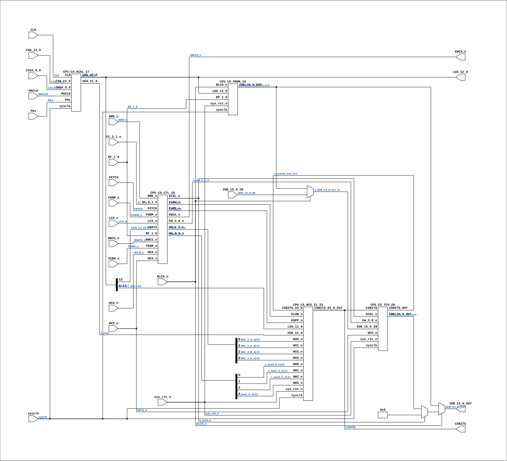
Contains: CPU_CS_ACAL_17, CPU_CS_CTL_18, CPU_CS_PROM_19, CPU_CS_TCV_20, CPU_CS_WCS_21_22
Module hierarchy - All modules
Schematic
Drawn from the Verilog: the yosys netlist of the Simulation (Verilator) build, instance CORE.CPU_BOARD.CPU.CS. Sub-modules are boxes (click the picture to open it full size; there every sub-module box links to its page, and every wire shows its Verilog name).
Description
ND120 CPU, MM&M CPU/CS CONTROL STORE SHEET 16 of 50 Last reviewed: 9-FEB-2025 Ronny Hansen
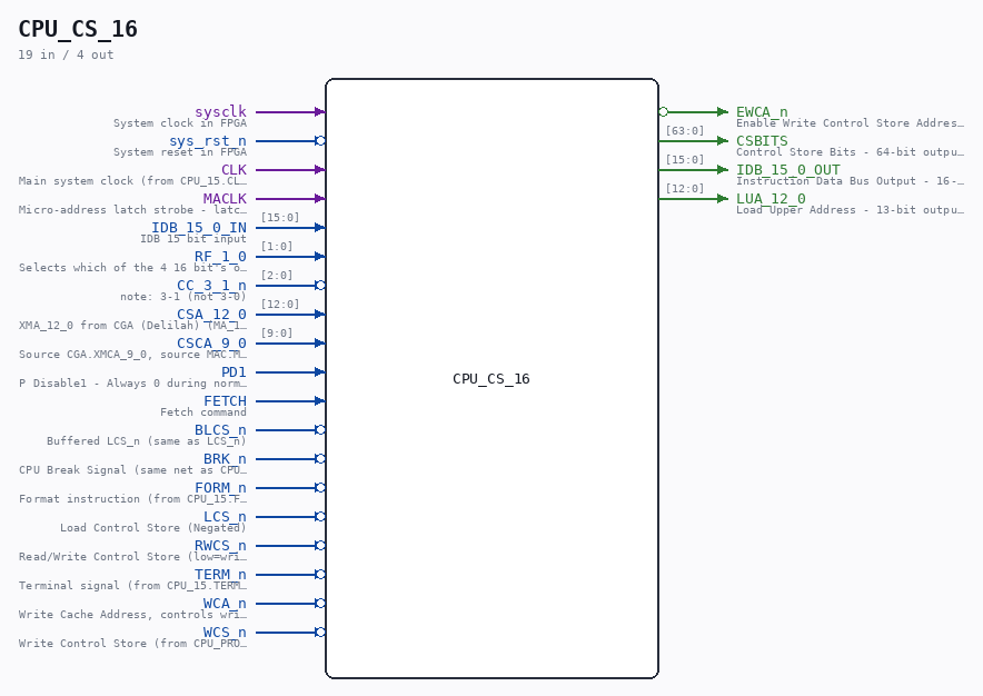
Ports
| Direction | Width | Name | Description |
|---|---|---|---|
| input | 1 |
sysclk |
System clock in FPGA |
| input | 1 |
sys_rst_n (active low) |
System reset in FPGA |
| input | 1 |
CLK |
Main system clock (from CPU_15.CLK) |
| input | 1 |
MACLK |
Micro-address latch strobe - latch enable for the control-store address latches in CPU_CS_ACAL_17 (transparent high, captures on the FALLING edge). (from CPU_15.MACLK) |
| input | [15:0] |
IDB_15_0_IN |
IDB 15 bit input |
| input | [1:0] |
RF_1_0 |
Selects which of the 4 16 bit's of the microcode to fetch from ROM (from CPU_PROC_32.RF_1_0) |
| input | [2:0] |
CC_3_1_n (active low) |
note: 3-1 (not 3-0) |
| input | [12:0] |
CSA_12_0 |
XMA_12_0 from CGA (Delilah) (MA_12_0 from CGA.MIC) <= Memory Address Bits (for Control Store) |
| input | [9:0] |
CSCA_9_0 |
Source CGA.XMCA_9_0, source MAC.MCA_9_0, source MAC_AP09.MCA_9_0, source CALCA.MCA9_0 <= Input ICA.Bits [15:0] but only when MCLK is low. Almost the same as LCA15_0, execpt LCA_15_0 is locked in a register on clock lo-hi |
| input | 1 |
PD1 |
P Disable1 - Always 0 during normal operations |
| input | 1 |
FETCH |
Fetch command |
| input | 1 |
BLCS_n (active low) |
Buffered LCS_n (same as LCS_n) |
| input | 1 |
BRK_n (active low) |
CPU Break Signal (same net as CPU_15.BRK_n) |
| input | 1 |
FORM_n (active low) |
Format instruction (from CPU_15.FORM_n) |
| input | 1 |
LCS_n (active low) |
Load Control Store (Negated) |
| input | 1 |
RWCS_n (active low) |
Read/Write Control Store (low=write) |
| input | 1 |
TERM_n (active low) |
Terminal signal (from CPU_15.TERM_n) |
| input | 1 |
WCA_n (active low) |
Write Cache Address, controls writing to the cache address register (from CPU_MMU_24.WCA_n) |
| input | 1 |
WCS_n (active low) |
Write Control Store (from CPU_PROC_32.WCS_n) |
| output | 1 |
EWCA_n (active low) |
Enable Write Control Store Address - Active low signal to enable writing to control store address |
| output | [63:0] |
CSBITS |
Control Store Bits - 64-bit output containing the control store data/instructions |
| output | [15:0] |
IDB_15_0_OUT |
Instruction Data Bus Output - 16-bit output bus for instruction data |
| output | [12:0] |
LUA_12_0 |
Load Upper Address - 13-bit output for upper address bits of control store |
Verilog source
Verilog/CPU-BOARD-3202/circuit/CPU_CS_16.v on GitHub.
Show the Verilog of CPU_CS_16 (200 lines)
/**************************************************************************
** ND120 CPU, MM&M                                                       **
** CPU/CS                                                                **
** CONTROL STORE                                                         **
** SHEET 16 of 50                                                        **
**                                                                       **
** Last reviewed: 9-FEB-2025                                             **
** Ronny Hansen                                                          **
***************************************************************************/

module CPU_CS_16 (
    // System Input signals
    input sysclk,    //! System clock in FPGA
    input sys_rst_n, //! System reset in FPGA

    // Clock signals
    input CLK,                    //! Main system clock (from CPU_15.CLK)
    input MACLK,                  //! Micro-address latch strobe - latch enable for the control-store address latches in CPU_CS_ACAL_17 (transparent high, captures on the FALLING edge). (from CPU_15.MACLK)

    // Input signals
    input [15:0] IDB_15_0_IN,  //! IDB 15 bit input
    input [1:0] RF_1_0,           //! Selects which of the 4 16 bit's of the microcode to fetch from ROM (from CPU_PROC_32.RF_1_0)
    input [2:0] CC_3_1_n,  // note: 3-1 (not 3-0)
    input [12:0] CSA_12_0,  //! XMA_12_0 from CGA (Delilah) (MA_12_0 from CGA.MIC) <= Memory Address Bits (for Control Store)
    input [9:0] CSCA_9_0, //! Source CGA.XMCA_9_0, source MAC.MCA_9_0, source MAC_AP09.MCA_9_0, source CALCA.MCA9_0 <= Input ICA.Bits [15:0] but only when MCLK is low. Almost the same as LCA15_0, execpt LCA_15_0 is locked in a register on clock lo-hi

    input PD1,   //! P Disable1 - Always 0 during normal operations
    input FETCH, //! Fetch command

    // FETCH: Source DECODE_DGA_COMM.FETCH, when Microcode command is:
    // 27 (JMP and CONTINUE)
    // 23+27 (C JMP)
    // 30 (AREAD COMMAND)
    // 32 & 33 (AWRITE)
    // 30 & 31 (AREAD)
    // 34 (READ & EXAMINE)
    // 35 (WRITE & DEPOSIT)
    // 22.0 (IREAD PT)
    // 22.1 (READ APT)
    // 22.3 (CNEXT.NWP)
    // 22.2 (MAP) - Address control store mapped as when FETCH. Used in Execute Register instruction (IDB contains instruction).

    input BLCS_n,   //! Buffered LCS_n (same as LCS_n)
    input BRK_n,                  //! CPU Break Signal (same net as CPU_15.BRK_n)
    input FORM_n,                 //! Format instruction (from CPU_15.FORM_n)
    input LCS_n,    //! Load Control Store (Negated)
    input RWCS_n,   //! Read/Write Control Store (low=write)
    input TERM_n,                 //! Terminal signal (from CPU_15.TERM_n)
    input WCA_n,                  //! Write Cache Address, controls writing to the cache address register (from CPU_MMU_24.WCA_n)
    input WCS_n,                  //! Write Control Store (from CPU_PROC_32.WCS_n)

    // Output signals
    output        EWCA_n,         //! Enable Write Control Store Address - Active low signal to enable writing to control store address
    output [63:0] CSBITS,         //! Control Store Bits - 64-bit output containing the control store data/instructions
    output [15:0] IDB_15_0_OUT,   //! Instruction Data Bus Output - 16-bit output bus for instruction data
    output [12:0] LUA_12_0        //! Load Upper Address - 13-bit output for upper address bits of control store
);

  /*******************************************************************************
   ** The wires are defined here                                                 **
   *******************************************************************************/
  wire [ 3:0] s_ew_3_0_n;
  wire [63:0] s_csbits_out_wcs;  // out from WCS — actual microcode word CPU executes
  wire [63:0] s_csbits_out_tcv;  // out from TCV

  wire [15:0] s_IDB_15_0_prom_out;
  wire [15:0] s_IDB_15_0_tcv_in;
  wire [15:0] s_IDB_15_0_tcv_out;

  wire [ 3:0] s_ww3_0_n;
  wire [ 3:0] s_WU_3_0_n;
  (* mark_debug = "true", DONT_TOUCH = "true" *) wire [12:0] s_LUA_12_0;

  wire [11:0] s_uua;
  wire        s_elow_n;
  wire        s_ecsl_n;
  wire        s_eupp_n;

  // Select the input data for the TCV (s_IDB_15_0_tcv_in) based on the BLCS_n signal:
  // - If BLCS_n is low, use data from the PROM (s_IDB_15_0_prom_out) for the TCV input.
  // - If BLCS_n is high, use the normal IDB data (IDB_15_0).
  assign s_IDB_15_0_tcv_in = BLCS_n ? IDB_15_0_IN : s_IDB_15_0_prom_out;


  /*******************************************************************************
   ** Here all output connections are defined                                    **
   *******************************************************************************/
  assign LUA_12_0 = s_LUA_12_0[12:0];

  // Output data bus selection for IDB_15_0_OUT:
  // - If BLCS_n is low (inactive high signal), output data is sourced from PROM.
  // - Otherwise, check ECSL_n for TCV data control:
  //   - If ECSL_n is low (inactive high signal), TCV data is output.
  //   - If ECSL_n is high, output is set to high-impedance state (tri-state).
  assign IDB_15_0_OUT = BLCS_n ?
                         (s_ecsl_n ? 16'b0 : s_IDB_15_0_tcv_out[15:0]) :
                         s_IDB_15_0_prom_out[15:0];


  // CSBITS out from this module is always the bits from OUT from the WCS/TCW (WCS is also feeding the TCV)
  //assign CSBITS = s_csbits_out_wcs | s_csbits_out_tcv;

    // CSBITS out is only from the writable-control-store
    assign CSBITS = s_csbits_out_wcs;

  /*******************************************************************************
   ** Here all sub-circuits are defined                                          **
   *******************************************************************************/

  CPU_CS_PROM_19 PROM (
      .sysclk(sysclk),
      .sys_rst_n(sys_rst_n),

      // Input signals
      .BLCS_n  (BLCS_n),
      .RF_1_0  (RF_1_0[1:0]),
      .LUA_12_0(s_LUA_12_0[12:0]),

      // Output signals
      .IDB_15_0_OUT(s_IDB_15_0_prom_out[15:0])
  );

  // CSBITS into WCS is always the CSBITS out from the TCV

  CPU_CS_WCS_21_22 WCS (
      // Input signals
      .sysclk(sysclk),
      .sys_rst_n(sys_rst_n),
      .CSBITS_63_0(s_csbits_out_tcv[63:0]),
      .ELOW_n(s_elow_n),
      .EUPP_n(s_eupp_n),
      .LUA_11_0(s_LUA_12_0[11:0]),
      .UUA_11_0(s_uua[11:0]),
      .WU0_n(s_WU_3_0_n[0]),
      .WU1_n(s_WU_3_0_n[1]),
      .WU2_n(s_WU_3_0_n[2]),
      .WU3_n(s_WU_3_0_n[3]),
      .WW0_n(s_ww3_0_n[0]),
      .WW1_n(s_ww3_0_n[1]),
      .WW2_n(s_ww3_0_n[2]),
      .WW3_n(s_ww3_0_n[3]),

      // Output signals
      .CSBITS_63_0_OUT(s_csbits_out_wcs[63:0])
  );

  CPU_CS_TCV_20 TCV (
      // Input signals
      .sysclk(sysclk),
      .sys_rst_n(sys_rst_n),
      .CSBITS(s_csbits_out_wcs[63:0]),
      .ECSL_n(s_ecsl_n),
      .EW_3_0_n(s_ew_3_0_n[3:0]),
      .IDB_15_0_IN(s_IDB_15_0_tcv_in[15:0]),
      .WCS_n(WCS_n),

      // Output signals
      .CSBITS_OUT(s_csbits_out_tcv[63:0]),
      .IDB_15_0_OUT(s_IDB_15_0_tcv_out[15:0])
  );

  CPU_CS_CTL_18 CTL (
      // Input signals
      .BRK_n(BRK_n),
      .CC_3_1_n(CC_3_1_n[2:0]),
      .EWCA_n(EWCA_n),
      .FETCH(FETCH),
      .FORM_n(FORM_n),
      .LCS_n(LCS_n),
      .LUA12(s_LUA_12_0[12]),
      .RF_1_0(RF_1_0[1:0]),
      .RWCS_n(RWCS_n),
      .TERM_n(TERM_n),
      .WCA_n(WCA_n),
      .WCS_n(WCS_n),

      // Output signals
      .ECSL_n(s_ecsl_n),
      .ELOW_n(s_elow_n),
      .EUPP_n(s_eupp_n),
      .EW_3_0_n(s_ew_3_0_n[3:0]),
      .WU_3_0_n(s_WU_3_0_n[3:0]),
      .WW_3_0_n(s_ww3_0_n[3:0])
  );

  CPU_CS_ACAL_17 ACAL (
      // Input signals
      .sysclk(sysclk),
      .CLK(CLK),
      .CSA_12_0(CSA_12_0[12:0]),
      .CSCA_9_0(CSCA_9_0[9:0]),
      .MACLK(MACLK),
      .PD1(PD1),
      // Output signals
      .LUA_12_0(s_LUA_12_0[12:0]),
      .UUA_11_0(s_uua[11:0])
  );

endmodule