CPU_MMU_CACHE_25
Source: Verilog/CPU-BOARD-3202/circuit/CPU_MMU_CACHE_25.v
Where it sits (Simulation): ND120_TOP > ND120_CORE > ND3202D > CPU_15 > CPU_MMU_24 > CPU_MMU_CACHE_25
- instance path: CORE.CPU_BOARD.CPU.MMU.CACHE
Used in: CPU_MMU_24 (all tops)
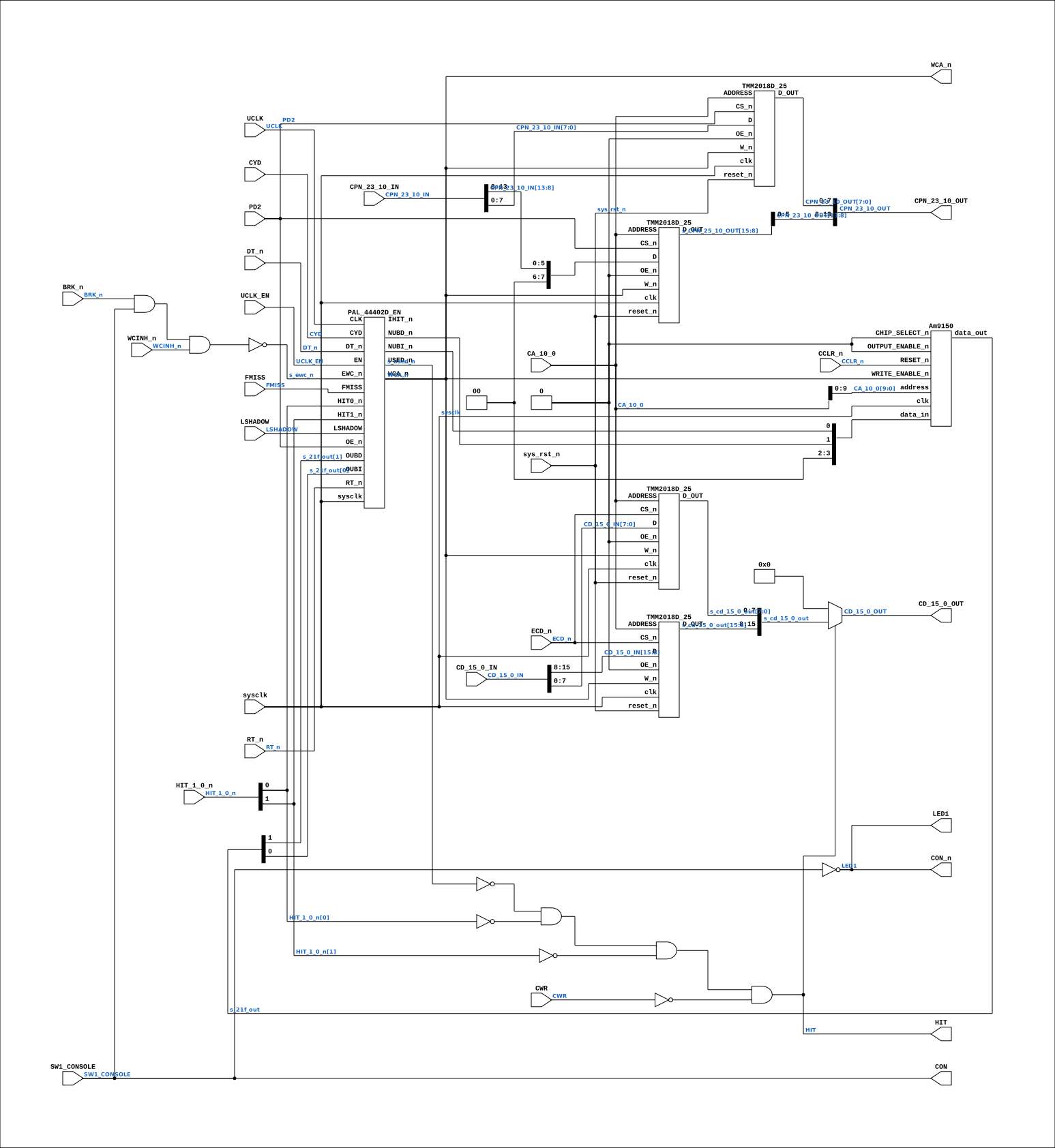
Contains: Am9150 (only on Simulation, Nexys, MEGA65 R6, MEGA65 R3, QMTECH, Basys3, Cmod), PAL_44402D_EN (only on Simulation, Nexys, MEGA65 R6, MEGA65 R3, QMTECH, Basys3, Cmod), TMM2018D_25 x4 (only on Simulation, Nexys, MEGA65 R6, MEGA65 R3, QMTECH, Basys3, Cmod)
Module hierarchy - All modules
Schematic
Drawn from the Verilog: the yosys netlist of the Simulation (Verilator) build, instance CORE.CPU_BOARD.CPU.MMU.CACHE. Sub-modules are boxes (click the picture to open it full size; there every sub-module box links to its page, and every wire shows its Verilog name).
Description
ND120 CPU, MM&M CPU/MMU/CACHE CACHE SHEET 25 of 50 Last reviewed: 2-FEB-2025 Ronny Hansen
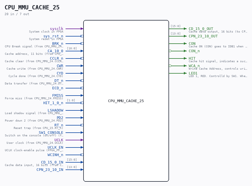
Ports
| Direction | Width | Name | Description |
|---|---|---|---|
| input | 1 |
sysclk |
System clock in FPGA |
| input | 1 |
sys_rst_n (active low) |
System reset in FPGA |
| input | 1 |
BRK_n (active low) |
CPU Break signal (from CPU_MMU_24.BRK_n) |
| input | [10:0] |
CA_10_0 |
Cache address, 11 bits (from CPU_MMU_24.CA_10_0) |
| input | 1 |
CCLR_n (active low) |
Cache clear (from CPU_MMU_24.CCLR_n) |
| input | 1 |
CWR |
Cache write (from CPU_MMU_24.CWR) |
| input | 1 |
CYD |
Cycle done (from CPU_MMU_24.CYD) |
| input | 1 |
DT_n (active low) |
Data transfer (from CPU_MMU_24.DT_n) |
| input | 1 |
ECD_n (active low) |
|
| input | 1 |
FMISS |
Force miss (from CPU_MMU_24.FMISS) |
| input | [1:0] |
HIT_1_0_n (active low) |
|
| input | 1 |
LSHADOW |
Load shadow signal (from CPU_MMU_24.LSHADOW) |
| input | 1 |
PD2 |
Power down 2 (from CPU_MMU_24.PD2) |
| input | 1 |
RT_n (active low) |
Reset trap (from CPU_15.RT_n) |
| input | 1 |
SW1_CONSOLE |
Switch on the console (on/off) (from CPU_MMU_24.SW1_CONSOLE) |
| input | 1 |
UCLK |
User clock (from CPU_MMU_24.UCLK) |
| input | 1 |
UCLK_EN |
UCLK clock-enable pulse (FPGA_FF_MODE, else 0) |
| input | 1 |
WCINH_n (active low) |
|
| input | [15:0] |
CD_15_0_IN |
Cache data input, 16 bits (from CPU_MMU_24.CD_15_0_IN) |
| output | [15:0] |
CD_15_0_OUT |
Cache data output, 16 bits (to CPU_MMU_24.CD_15_0_OUT) |
| input | [13:0] |
CPN_23_10_IN |
|
| output | [13:0] |
CPN_23_10_OUT |
|
| output | 1 |
CON |
Cache ON (CON) goes to IDB1 when ECSR_n is low. CON_n goes to IDB2 (to CPU_MMU_CSR_26.CON) |
| output | 1 |
CON_n (active low) |
|
| output | 1 |
HIT |
Cache hit signal, indicates a successful cache lookup (to CPU_MMU_24.HIT) |
| output | 1 |
WCA_n (active low) |
Write Cache Address, controls writing to the cache address register (to CPU_MMU_24.WCA_n) |
| output | 1 |
LED1 |
LED 1, RED. Controlld by SW1. When LED is on, CON is 0. and CON_n is 1. |
Verilog source
Verilog/CPU-BOARD-3202/circuit/CPU_MMU_CACHE_25.v on GitHub.
Show the Verilog of CPU_MMU_CACHE_25 (342 lines)
/**************************************************************************
** ND120 CPU, MM&M                                                       **
** CPU/MMU/CACHE                                                         **
** CACHE                                                                 **
** SHEET 25 of 50                                                        **
**                                                                       **
** Last reviewed: 2-FEB-2025                                             **
** Ronny Hansen                                                          **
***************************************************************************/


module CPU_MMU_CACHE_25 (

    input sysclk,    // System clock in FPGA
    input sys_rst_n, // System reset in FPGA

    input        BRK_n,  //! CPU Break signal (from CPU_MMU_24.BRK_n)
    input [10:0] CA_10_0,  //! Cache address, 11 bits (from CPU_MMU_24.CA_10_0)
    input        CCLR_n,  //! Cache clear (from CPU_MMU_24.CCLR_n)
    input        CWR,  //! Cache write (from CPU_MMU_24.CWR)
    input        CYD,  //! Cycle done (from CPU_MMU_24.CYD)
    input        DT_n,  //! Data transfer (from CPU_MMU_24.DT_n)
    input        ECD_n,
    input        FMISS,  //! Force miss (from CPU_MMU_24.FMISS)
    input [ 1:0] HIT_1_0_n,
    input        LSHADOW,  //! Load shadow signal (from CPU_MMU_24.LSHADOW)
    input        PD2,  //! Power down 2 (from CPU_MMU_24.PD2)
    input        RT_n,  //! Reset trap (from CPU_15.RT_n)
    input        SW1_CONSOLE,  //! Switch on the console (on/off) (from CPU_MMU_24.SW1_CONSOLE)
    input        UCLK,  //! User clock (from CPU_MMU_24.UCLK)
    input        UCLK_EN,  //! UCLK clock-enable pulse (FPGA_FF_MODE, else 0)
    input        WCINH_n,

    input  [15:0] CD_15_0_IN,  //! Cache data input, 16 bits (from CPU_MMU_24.CD_15_0_IN)
    output [15:0] CD_15_0_OUT,  //! Cache data output, 16 bits (to CPU_MMU_24.CD_15_0_OUT)

    input  [13:0] CPN_23_10_IN,
    output [13:0] CPN_23_10_OUT,

    /*******************************************************************************
   ** The outputs are defined here                                               **
   *******************************************************************************/

    output CON,      //! Cache ON (CON) goes to IDB1 when ECSR_n is low. CON_n goes to IDB2 (to CPU_MMU_CSR_26.CON)
    output CON_n,
    output HIT,      //! Cache hit signal, indicates a successful cache lookup (to CPU_MMU_24.HIT)
    output WCA_n,    //! Write Cache Address, controls writing to the cache address register (to CPU_MMU_24.WCA_n)

    output LED1  //LED 1, RED. Controlld by SW1. When LED is on, CON is 0. and CON_n is 1.
);


  /*******************************************************************************
   ** The wires are defined here                                                 **
   *******************************************************************************/
  wire [15:0] s_cd_15_0_out;
  wire [10:0] s_ca_10_0;
  wire [ 1:0] s_hit_1_0_n;
  wire        s_wca_n   /* verilator public_flat_rd */;   // probed by runSim (cache log)
  wire        s_brk_n;
  wire        s_wcinh_n;
  wire        s_used_n;
  wire        s_con;
  wire        s_con_n;
  wire        s_cclr_n  /* verilator public_flat_rd */;   // probed by runSim (cache log)
  wire        s_hit;
  wire        s_dt_n    /* verilator public_flat_rd */;   // probed by runSim (cache log)
  wire        s_lshadow;
  wire        s_cyd;
  wire        s_cwr;
  wire        s_uclk;
  wire        s_rt_n    /* verilator public_flat_rd */;   // probed by runSim (cache log)
  wire        s_pd2     /* verilator public_flat_rd */;   // probed by runSim (cache log)
  wire        s_fmiss;
  wire        s_ecd_n;
  wire        s_ewc_n;
  wire        s_gnd;


  wire [15:0] s_CPN_25_10_OUT;
  wire [ 3:0] s_21f_in  /* verilator public_flat_rd */;   // probed by runSim (cache log)
  wire [ 3:0] s_21f_out;


  /*******************************************************************************
   ** Here all input connections are defined                                     **
   *******************************************************************************/
  assign s_ca_10_0 = CA_10_0;
  assign s_hit_1_0_n[1:0] = HIT_1_0_n;
`ifdef ND120_NO_CACHE
  // CACHE COMPILED OUT (-DND120_NO_CACHE).
  //
  // This is NOT an invented mode: the board has SW1, a real cache on/off
  // switch, and CON low IS the off position. So the machine reports its cache
  // status as DISABLED exactly as it would with the switch thrown, LED1 lit,
  // and the hit comparators held disabled - and every access goes to main
  // memory. What the define adds on top is that the cache SRAMs and the
  // used-bit PAL are not instantiated at all, so the logic is not merely
  // bypassed, it is absent.
  //
  // Why it exists: on the Tang Nano 20K the design does not fit with the
  // cache present. Ignore SW1_CONSOLE and force the off position.
  assign s_con = 1'b0;
`else
  assign s_con = SW1_CONSOLE;
`endif
  assign s_brk_n = BRK_n;
  assign s_wcinh_n = WCINH_n;
  assign s_cclr_n = CCLR_n;
  assign s_dt_n = DT_n;
  assign s_lshadow = LSHADOW;
  assign s_cyd = CYD;
  assign s_cwr = CWR;
  assign s_uclk = UCLK;
  assign s_rt_n = RT_n;
  assign s_pd2 = PD2;
  assign s_fmiss = FMISS;
  assign s_ecd_n = ECD_n;

  /*******************************************************************************
   ** Here all output connections are defined                                    **
   *******************************************************************************/
  // Banner word-index-2 fix (26-JUL): the cache data SRAM (23F/24F) is driven onto
  // the wired-OR CD bus for the whole read-transfer (CS=ECD, sheet 25). On a MISS the
  // memory data only survives that OR because the refill (WCA) forces the SRAM output
  // to 0 while writing. For a CACHE-INHIBIT page (WCINH) the refill is suppressed, so a
  // line still holding stale non-zero data (e.g. 0177777 cached during init-clear, then
  // the memory rewritten by DMA which bypasses the cache) JAMS the OR bus over the
  // correct memory word -> banner "INSTRUCTION" printed as "INST\x7f\x7fCTION".
  // Gate the cache CD output by HIT so it contributes 0 unless this line genuinely
  // matches the requested address; memory then passes cleanly on every miss/inhibit.
  // Escape hatch: -DND120_CACHE_DRIVE_UNGATED restores the raw schematic behaviour.
`ifdef ND120_NO_CACHE
  // No cache RAM exists in this build, so the sheet contributes nothing to the
  // wired-OR CD bus and memory data passes cleanly on every access.
  assign CD_15_0_OUT = 16'b0;
`elsif ND120_CACHE_DRIVE_UNGATED
  assign CD_15_0_OUT = s_cd_15_0_out[15:0];
`else
  assign CD_15_0_OUT = s_hit ? s_cd_15_0_out[15:0] : 16'b0;
`endif
  assign CON = s_con;
  assign CON_n = s_con_n;
  assign HIT = s_hit;
  assign WCA_n = s_wca_n;

  assign CPN_23_10_OUT = s_CPN_25_10_OUT[13:0];


  // Code to make LINTER not complaing about bits not read in CPN 25:10 (which is none-existsing)
  (* keep = "true", DONT_TOUCH = "true" *) wire [1:0] unused_CPN_bits;
  assign unused_CPN_bits[1:0] =  s_CPN_25_10_OUT[15:14];

  /*******************************************************************************
   ** Here all in-lined components are defined                                   **
   *******************************************************************************/

  // Ground
  assign s_gnd = 1'b0;
  assign s_con_n = ~s_con;

  // Led1 cathode is connected to CON signal, and ANODE to VCC, so a low on s_CON will give light in LED1
  assign LED1      = s_con_n;

  /*******************************************************************************
   ** Here all normal components are defined                                     **
   *******************************************************************************/
  /*
   NAND_GATE_3_INPUTS #(.BubblesMask(3'b000))
      GATES_1 (.input1(s_brk_n),
               .input2(s_con),
               .input3(s_wcinh_n),
               .result(s_ewc_n));
   */

  assign s_ewc_n = ~(s_brk_n & s_con & s_wcinh_n);

  /*
   AND_GATE_5_INPUTS #(.BubblesMask({1'b1, 4'hF}))
      GATES_2 (.input1(s_used_n),
               .input2(s_hit_1_0_n[1]),
               .input3(s_hit_1_0_n[0]),
               .input4(s_cwr),
               .input5(s_gnd), //GND
               .result(s_hit));
   */

`ifdef ND120_NO_CACHE
  // With CON forced to the off position the comparators on sheet 27 are held
  // disabled and report NO MATCH, so this is 0 by the same logic the switch
  // gives. Stated directly here so no cache signal is left undriven once the
  // RAMs below are omitted.
  assign s_hit = 1'b0;
`else
  assign s_hit = !s_used_n & !s_hit_1_0_n[0] & !s_hit_1_0_n[1] & !s_cwr;
`endif
  /*******************************************************************************
   ** Here all sub-circuits are defined                                          **
   *******************************************************************************/

`ifdef ND120_NO_CACHE
  // The five cache memories (23F/24F data, 16F/20F tag, 21F used-bits) and the
  // used-bit PAL 18F are NOT INSTANTIATED in this build. Everything they drive
  // is given its cache-off constant here.
  assign s_cd_15_0_out    = 16'b0;
  assign s_CPN_25_10_OUT  = 16'b0;
  assign s_used_n         = 1'b1;   // no line is "used"
  assign s_wca_n          = 1'b1;   // never write a cache address
`else

  //  16K bit Static RAM  (2KByte) - ASYNC read, see the parameter in TMM2018D_25.v
  TMM2018D_25 #(.ASYNC_READ(1)) CHIP_23F
  (
    .clk    (sysclk),               // Clock input (BLOCK RAM MUST HAVE CLOCK)
    .reset_n(sys_rst_n),            // FPGA Reset input (active low)

    // Input signals
    .ADDRESS(s_ca_10_0[10:0]),
    .CS_n   (s_ecd_n),
    .OE_n   (s_gnd),
    .W_n    (s_wca_n),

    // Bus data in and out
    .D      (CD_15_0_IN[15:8]),
    .D_OUT  (s_cd_15_0_out[15:8])
  );

  //  16K bit Static RAM  (2KByte)
  TMM2018D_25 #(.ASYNC_READ(1)) CHIP_24F
  (
    .clk    (sysclk),              // Clock input (BLOCK RAM MUST HAVE CLOCK)
    .reset_n(sys_rst_n),           // FPGA Reset input (active low)

     // Input signals
    .ADDRESS(s_ca_10_0[10:0]),
    .CS_n   (s_ecd_n),
    .OE_n   (s_gnd),
    .W_n    (s_wca_n),

    // Bus data in and out
    .D      (CD_15_0_IN[7:0]),
    .D_OUT  (s_cd_15_0_out[7:0])
  );

  // P3 (docs/plan-fix-unconstrained-clocks.md): in FF mode the UBITS PAL
  // registers capture on posedge sysclk gated by the rise-aligned UCLK
  // enable instead of clocking on the routed s_uclk net (uclk_Z clock root).
`ifdef FPGA_FF_MODE
  localparam UCLK_CE = 1;
`else
  localparam UCLK_CE = 0;
`endif

  PAL_44402D_EN #(.USE_ENABLE(UCLK_CE)) PAL_44402_UBITS (  // PAL16R4D
      .sysclk(sysclk),
      .EN(UCLK_EN),
      .CLK (s_uclk),
      .OE_n(s_pd2),

      .DT_n(s_dt_n),
      .RT_n(s_rt_n),
      .LSHADOW(s_lshadow),
      .FMISS(s_fmiss),
      .CYD(s_cyd),
      .HIT0_n(s_hit_1_0_n[0]),
      .HIT1_n(s_hit_1_0_n[1]),
      .EWC_n(s_ewc_n),

      .USED_n(s_used_n),
      .WCA_n (s_wca_n),
      .OUBI  (s_21f_out[0]),
      .OUBD  (s_21f_out[1]),


      .NUBI_n(s_21f_in[0]),
      .NUBD_n(s_21f_in[1]),

      //.Q2_n(), // Not connected
      .IHIT_n()  //.Q3_n(s_ihit) // IHIT_n not connected
  );

  assign s_21f_in[3:2] = 2'b00;

// Code to make LINTER _not_ complain about bits not read in s_21f_out bits 3 and 2
  (* keep = "true", DONT_TOUCH = "true" *) wire [1:0] unused_21f_out_bits;
  assign unused_21f_out_bits[1:0] = s_21f_out[3:2];

  // 4KBit * 4 DYNAMIC RAM
  Am9150 CHIP_21F
  (
      .clk            (sysclk),          // Clock input (BLOCK RAM MUST HAVE CLOCK)
      .address        (s_ca_10_0[9:0]),
      .OUTPUT_ENABLE_n(s_gnd),
      .RESET_n        (s_cclr_n),
      .CHIP_SELECT_n  (s_gnd),
      .WRITE_ENABLE_n (s_wca_n),

      .data_in        (s_21f_in[3:0]),
      .data_out       (s_21f_out[3:0])
  );

  //  16K bit Static RAM  (2KByte)
  TMM2018D_25 #(.ASYNC_READ(1)) CHIP_16F
  (
    .clk(sysclk),  // Clock input (BLOCK RAM MUST HAVE CLOCK)
    .reset_n(sys_rst_n),  // FPGA Reset input (active low)

     // Input signals
    .ADDRESS(s_ca_10_0[10:0]),
    .CS_n(s_pd2),
    .OE_n(s_gnd),
    .W_n(s_wca_n),

    // Bus data in and out
    .D({
    2'b00, CPN_23_10_IN[13:8]
    }),  // bit D0 and D1 is not connected (we need only 6 bits) for CPN 23-18
    .D_OUT(s_CPN_25_10_OUT[15:8]) // CPN 25:10. CPN 25 and 24 is none existsting and not connected in the schema.
  );

  //  16K bit Static RAM  (2KByte)
  TMM2018D_25 #(.ASYNC_READ(1)) CHIP_20F
  (
    .clk    (sysclk),                // Clock input (BLOCK RAM MUST HAVE CLOCK)
    .reset_n(sys_rst_n),             // FPGA Reset input (active low)

    // Input signals
    .ADDRESS(s_ca_10_0[10:0]),
    .CS_n   (s_pd2),
    .OE_n   (s_gnd),
    .W_n    (s_wca_n),

      // Bus data in and out
    .D      (CPN_23_10_IN[7:0]),
    .D_OUT  (s_CPN_25_10_OUT[7:0])  // CPN 17-10

  );
`endif  // ND120_NO_CACHE

endmodule