MEM_DATA_46
Source: Verilog/CPU-BOARD-3202/circuit/MEM_DATA_46.v
Where it sits (Simulation): ND120_TOP > ND120_CORE > ND3202D > MEM_43 > MEM_DATA_46
- instance path: CORE.CPU_BOARD.MEM.DATA
Used in: MEM_43 (all tops)
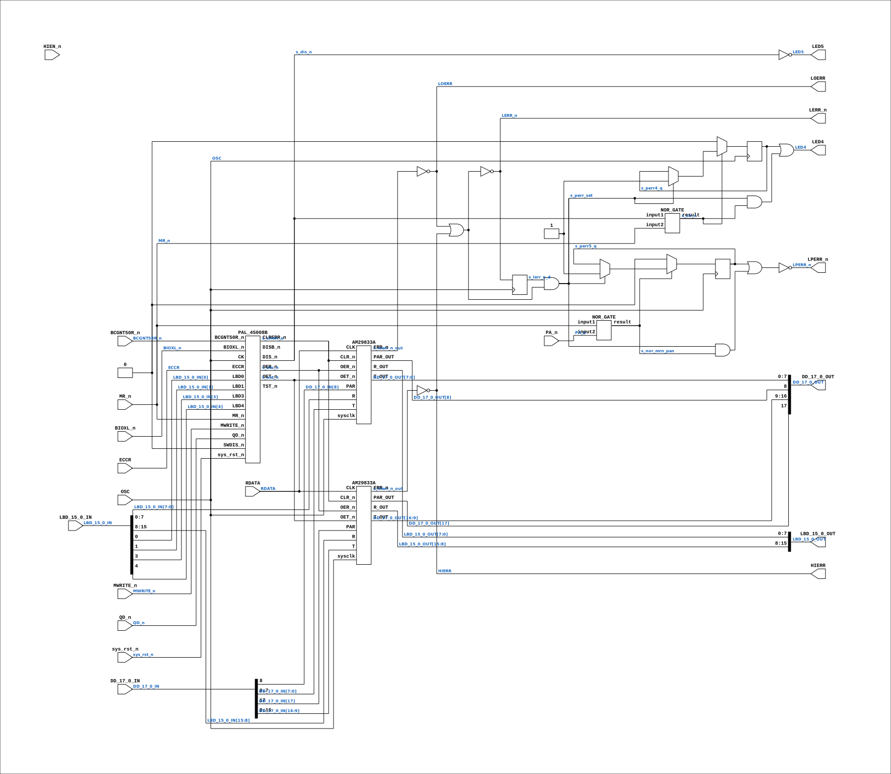
Contains: AM29833A x2, NOR_GATE x2, PAL_45008B
Module hierarchy - All modules
Schematic
Drawn from the Verilog: the yosys netlist of the Simulation (Verilator) build, instance CORE.CPU_BOARD.MEM.DATA. Sub-modules are boxes (click the picture to open it full size; there every sub-module box links to its page, and every wire shows its Verilog name).
Description
ND120 CPU, MM&M MEM/DATA DATA & PARITY TCV SHEET 46 of 50 Last reviewed: 22-MAR-2025 Ronny Hansen
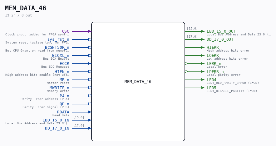
Ports
| Direction | Width | Name | Description |
|---|---|---|---|
| input | 1 |
OSC |
Clock input (added for FPGA synthesis) |
| input | 1 |
sys_rst_n (active low) |
System reset (active low, for FPGA synthesis) |
| input | 1 |
BCGNT50R_n (active low) |
Bus CPU Grant on read from memory after the address (from 50 ns after GNT on read cycle) |
| input | 1 |
BIOXL_n (active low) |
Bus IOX Enable |
| input | 1 |
ECCR |
Bus ECC Request |
| input | 1 |
HIEN_n (active low) |
High address bits enable (not used) |
| input | 1 |
MR_n (active low) |
Master reset |
| input | 1 |
MWRITE_n (active low) |
Memory Write |
| input | 1 |
PA_n (active low) |
Parity Error Address (PEA) |
| input | 1 |
QD_n (active low) |
Parity Error Signal (PES) |
| input | 1 |
RDATA |
Read Data |
| input | [15:0] |
LBD_15_0_IN |
Local Bus Address and Data 23:0 (IN) - Address and Data for RAM (from MEM_43.LBD_23_0_IN[15:0]) |
| output | [15:0] |
LBD_15_0_OUT |
Local Bus Address and Data 23:0 (OUT) - Data from from RAM (15:0) (to MEM_43.LBD_23_0_OUT[15:0]) |
| input | [17:0] |
DD_17_0_IN |
|
| output | [17:0] |
DD_17_0_OUT |
|
| output | 1 |
HIERR |
High address bits error |
| output | 1 |
LOERR |
Low address bits error |
| output | 1 |
LERR_n (active low) |
Local error |
| output | 1 |
LPERR_n (active low) |
Local parity error |
| output | 1 |
LED4 |
LED4_RED_PARITY_ERROR (1=ON) |
| output | 1 |
LED5 |
LED5_DISABLE_PARTITY (1=ON) |
Verilog source
Verilog/CPU-BOARD-3202/circuit/MEM_DATA_46.v on GitHub.
Show the Verilog of MEM_DATA_46 (331 lines)
/**************************************************************************
** ND120 CPU, MM&M                                                       **
** MEM/DATA                                                              **
** DATA & PARITY TCV                                                     **
** SHEET 46 of 50                                                        **
**                                                                       **
** Last reviewed: 22-MAR-2025                                            **
** Ronny Hansen                                                          **
***************************************************************************/

module MEM_DATA_46 (
    input OSC,         //! Clock input (added for FPGA synthesis)
    input sys_rst_n,   //! System reset (active low, for FPGA synthesis)

    // Input signals
    input BCGNT50R_n,  //! Bus CPU Grant on read from memory after the address (from 50 ns after GNT on read cycle)
    input BIOXL_n,     //! Bus IOX Enable
    input ECCR,        //! Bus ECC Request
    input HIEN_n,      //! High address bits enable (not used)
    input MR_n,        //! Master reset
    input MWRITE_n,    //! Memory Write
    input PA_n,        //! Parity Error Address (PEA)
    input QD_n,        //! Parity Error Signal (PES)
    input RDATA,       //! Read Data

    // IN and OUT signals
    input  [15:0] LBD_15_0_IN,  //! Local Bus Address and Data 23:0 (IN) -  Address and Data for RAM (from MEM_43.LBD_23_0_IN[15:0])
    output [15:0] LBD_15_0_OUT,  //! Local Bus Address and Data 23:0 (OUT) - Data from from RAM (15:0) (to MEM_43.LBD_23_0_OUT[15:0])

    input  [17:0] DD_17_0_IN,
    output [17:0] DD_17_0_OUT,

    // Output signals
    output HIERR,       //! High address bits error
    output LOERR,       //! Low address bits error
    output LERR_n,      //! Local error
    output LPERR_n,     //! Local parity error
    output LED4,        //! LED4_RED_PARITY_ERROR (1=ON)
    output LED5         //! LED5_DISABLE_PARTITY (1=ON)
);


  /*******************************************************************************
   ** The wires are defined here                                                 **
   *******************************************************************************/
  wire        s_osc;
  wire [15:0] s_lbd_15_0_in;
  wire [15:0] s_lbd_15_0_out;
  wire [17:0] s_dd_17_0_in;
  wire [17:0] s_dd_17_0_out;
  wire        s_bcgnt50r_n;
  wire        s_bioxl_n;
  wire        s_clr_14_8j;
  wire        s_clr_15_8j;
  wire        s_clr_n;
  wire        s_clrerr_n;
  wire        s_dis_n;
  wire        s_eccr;
  wire        s_gnd;
  wire        s_hierr_n_out;
  wire        s_hierr_out;
  wire        s_led4;
  wire        s_lerr_n_out;
  wire        s_loerr_n_out;
  wire        s_loerr_out;
  wire        s_lperr_n_out;
  wire        s_mr_n;
  wire        s_mwrite_n;
  wire        s_nor_mrn_pan;
  wire        s_oer_n;
  wire        s_oet_n;
  wire        s_pa_n;
  wire        s_power;
  wire        s_qd_n;
  wire        s_rdata;

  // Unused wires, this to keep LINTER happy and not complaining about bits not read
  (* keep = "true", DONT_TOUCH = "true" *) wire s_hien_n;

  /*******************************************************************************
   ** Here all input connections are defined                                     **
   *******************************************************************************/
  assign s_osc               = OSC;
  assign s_lbd_15_0_in[15:0] = LBD_15_0_IN;
  assign s_dd_17_0_in[17:0]  = DD_17_0_IN;
  assign s_rdata             = RDATA;
  assign s_bioxl_n           = BIOXL_n;
  assign s_bcgnt50r_n        = BCGNT50R_n;
  assign s_pa_n              = PA_n;
  assign s_qd_n              = QD_n;
  assign s_mr_n              = MR_n;
  assign s_eccr              = ECCR;
  assign s_hien_n            = HIEN_n;
  assign s_mwrite_n          = MWRITE_n;

  /*******************************************************************************
   ** Here all output connections are defined                                    **
   *******************************************************************************/
  assign DD_17_0_OUT         = s_dd_17_0_out[17:0];
  assign HIERR               = s_hierr_out;
  assign LERR_n              = s_lerr_n_out;
  assign LOERR               = s_loerr_out;
  assign LPERR_n             = s_lperr_n_out;
  assign LBD_15_0_OUT        = s_lbd_15_0_out[15:0];

  /*******************************************************************************
   ** Here all in-lined components are defined                                   **
   *******************************************************************************/

  // Ground
  assign s_gnd               = 1'b0;

  // Power
  assign s_power             = 1'b1;

  // NOT Gate
  assign s_clr_15_8j         = ~s_clr_n;
  assign s_clr_14_8j         = ~s_nor_mrn_pan;

  // Sheet 46, region E2-F3: the AM29833A ERR pins (1H pin 10, 2H pin 10) are
  // OPEN COLLECTOR, pulled up by R21/R26, and feed the 74F04 (1F) directly -
  // pin 1->2 = LOERR, pin 3->4 = HIERR. Nothing on the drawing gates them.
  //
  // These were gated by OET_n, and OET_n = MWRITE_n (PAL 45008), so OET_n high
  // is precisely a READ - the one case where a stored parity error would be
  // reported. A memory error could therefore never raise LERR~, never set the
  // PES bits and never light LED4.
  //
  // That matters beyond fidelity: the CONFIGURATION diagnostic decides whether
  // a memory bank is LOCAL or MULTIPORT by arming the ECC-simulate probe and
  // waiting for a level-14 parity interrupt. Silence means "Mpm 5". Measured
  // 11-AUG-2026 on the Tang: all 4 MB reports as Mpm 5, and SINTRAN then treats
  // a page fault in it as a fault in the ND-500/5000 shared-memory window,
  // which is fatal on a machine with no ND-500.
  //
  // NOTE: this restores the REPORTING path only. With parity recomputed on
  // every read (ND_SDRAM_PACK16) no error can be generated, so behaviour does
  // not change until the ECCR simulate path exists.
  assign s_loerr_out         = ~s_loerr_n_out;
  assign s_hierr_out         = ~s_hierr_n_out;

  // LED: LED4_RED_PARITY_ERROR
  assign LED4                = ~s_led4;
  // LED: LED5_DISABLE_PARITY
  assign LED5                = ~s_dis_n;
  /*******************************************************************************
   ** Here all normal components are defined                                     **
   *******************************************************************************/
  NOR_GATE #(
      .BubblesMask(2'b11)
  ) GATES_1 (
      .input1(s_dis_n),
      .input2(s_mr_n),
      .result(s_clr_n)
  );

  NOR_GATE #(
      .BubblesMask(2'b11)
  ) GATES_2 (
      .input1(s_mr_n),
      .input2(s_pa_n),
      .result(s_nor_mrn_pan)
  );

  /*
  NOR_GATE #(
      .BubblesMask(2'b00)
  ) GATES_3 (
      .input1(s_loerr_out),
      .input2(s_hierr_out),
      .result(s_lerr_n_out)
  );
  */
  assign s_lerr_n_out= ~(s_loerr_out | s_hierr_out);

  // MEMORY_4/MEMORY_5 hold the parity-error state (LED4 and LPERR_n). The
  // original chips are J-K flip-flops CLOCKED by LERR_n - a combinational
  // net (s_lerr_n_out = ~(LOERR | HIERR)). On FPGA that is an unconstrained
  // fabric clock rooted in the AM29833A regERR FFs (check_timing no_clock,
  // Place 30-568, measured 21-AUG-2026). In FF mode, replace with the same
  // sysclk edge-capture pattern AM29833A itself uses (gen_sysclk_edge):
  // sample LERR_n on s_osc, set on its falling edge (j=1, k=0), reset wins.
  // Latch mode keeps the original J-K chips.
`ifdef FPGA_FF_MODE
  reg s_lerr_n_d = 1'b1;
  reg s_perr4_q = 1'b0;    // MEMORY_4 state (q); s_led4 is qBar
  reg s_perr5_q = 1'b0;    // MEMORY_5 state (q); s_lperr_n_out is qBar
  // Pending falling edge of LERR_n, visible combinationally the moment it
  // falls (the original J-K sets ON the edge, not a clock later); registered
  // at the next s_osc edge. s_lerr_n_d is an FF, so this adds no loop.
  wire s_perr_set = s_lerr_n_d & ~s_lerr_n_out & s_power;
  always @(posedge s_osc) begin
    s_lerr_n_d <= s_lerr_n_out;
    if (s_clr_15_8j)      s_perr4_q <= 1'b0;
    else if (s_perr_set)  s_perr4_q <= 1'b1;
    if (s_clr_14_8j)      s_perr5_q <= 1'b0;
    else if (s_perr_set)  s_perr5_q <= 1'b1;
  end
  assign s_led4        = ~(s_perr4_q | (s_perr_set & ~s_clr_15_8j));
  assign s_lperr_n_out = ~(s_perr5_q | (s_perr_set & ~s_clr_14_8j));
`else
  J_K_FLIPFLOP #(
      .InvertClockEnable(1)
  ) MEMORY_4 (
      .clock(s_lerr_n_out),
      .j(s_power),
      .k(s_gnd),
      .preset(s_gnd),
      .q(),
      .qBar(s_led4), // LED4 PARITY ERROR
      .reset(s_clr_15_8j),
      .tick(1'b1)
  );

  J_K_FLIPFLOP #(
      .InvertClockEnable(1)
  ) MEMORY_5 (
      .clock(s_lerr_n_out),
      .j(s_power),
      .k(s_gnd),
      .preset(s_gnd),
      .q(),
      .qBar(s_lperr_n_out),
      .reset(s_clr_14_8j),
      .tick(1'b1)
  );
`endif


  /*******************************************************************************
   ** Here all sub-circuits are defined                                          **
   *******************************************************************************/


  PAL_45008B PAL_45008_UDATA (
      .CK      (s_osc),         //! Clock (added for FPGA synthesis)
      .sys_rst_n(sys_rst_n),    //! System reset (for FPGA synthesis)

      .MWRITE_n(s_mwrite_n),  //! I0 - MWRITE_n
      .SWDIS_n   (s_gnd),       //! I1 - SWDIS_n (SW4 - Parity disable, normal position = down. HERE: Disabled!)
      .LBD0(s_lbd_15_0_in[0]),  //! I2 - LBD0
      .LBD1(s_lbd_15_0_in[1]),  //! I3 - LBD1
      .LBD3(s_lbd_15_0_in[3]),  //! I4 - LBD3
      .LBD4(s_lbd_15_0_in[4]),  //! I5 - LBD4
      .BIOXL_n(s_bioxl_n),  //! I6 - BIOXL_n
      .ECCR(s_eccr),  //! I7 - ECCR
      .BCGNT50R_n(s_bcgnt50r_n),  //! I8 - BCGNT50R_n
      //.HIEN_n(s_hien_n),  //! I9 - EPEA_n  (NOT USED!)

      .DIS_n(s_dis_n),  //! DIS_n Y0_n (OUT Only) (LED5 Disable Parity)
      .OER_n(s_oer_n),  //! OER_n Y1_n (OUT ONLY)

      .OET_n   (s_oet_n),     //! B0_n - OET_n
      .CLRERR_n(s_clrerr_n),  //! B1_n - CLRERR_n
      .DISB_n  (),            //! B2_n - DISB_n (n.c)
      .TST_n   (),            //! B3_n - TST_n (n.c.)
      .QD_n    (s_qd_n),      //! B4_n - QD_n
      .MR_n    (s_mr_n)       //! B5_n - MR_n
  );


  // RDATA is a read-data strobe generated in the OSC domain (PAL_44310), not
  // a clock. Clocking the parity-error registers on `posedge RDATA` makes
  // RDATA a fabric-routed clock net on FPGA (unconstrained, hold-race
  // lottery - see docs/plan-fix-unconstrained-clocks.md P1a). In FF mode use
  // the sysclk-sampled edge capture instead (OSC == sysclk on FPGA); latch
  // mode keeps the original chip behavior.
`ifdef FPGA_FF_MODE
  localparam PARITY_ERR_CAPTURE = 2;
`else
  localparam PARITY_ERR_CAPTURE = 0;
`endif

  AM29833A #(.USE_SYSCLK(PARITY_ERR_CAPTURE)) CHIP_1H (
      .sysclk(s_osc),
      .CLK(s_rdata),
      .CLR_n(s_clrerr_n),
      .ERR_n(s_loerr_n_out),  // output (pulled high) // TODO: Fix pull up when output is not enabled
      .OER_n(s_oer_n),
      .OET_n(s_oet_n),

      // PARITY IN
      .PAR(s_dd_17_0_in[8]),

      // PARITY OUT
      .PAR_OUT(s_dd_17_0_out[8]),

      // R IN
      .R(s_lbd_15_0_in[7:0]),

      // R out
      .R_OUT(s_lbd_15_0_out[7:0]),

      // T in
      .T(s_dd_17_0_in[7:0]),

      // T out + T[8] = PAR // TODO: Pull high when OET is disabled
      .T_OUT(s_dd_17_0_out[7:0])
  );

  AM29833A #(.USE_SYSCLK(PARITY_ERR_CAPTURE)) CHIP_2H (
      .sysclk(s_osc),
      .CLK(s_rdata),
      .CLR_n(s_clrerr_n),
      .ERR_n  (s_hierr_n_out),        // output (pulled high) // TODO: Fix pull up when output is not enabled
      .OER_n(s_oer_n),
      .OET_n(s_oet_n),

      // PARITY in
      .PAR(s_dd_17_0_in[17]),

      // PARITY out
      .PAR_OUT(s_dd_17_0_out[17]),

      // R in
      .R(s_lbd_15_0_in[15:8]),

      // R out
      .R_OUT(s_lbd_15_0_out[15:8]),

      // T in
      .T(s_dd_17_0_in[16:9]),

      // T out + T[17] = PAR  // TODO: Pull high when OET is disabled
      .T_OUT(s_dd_17_0_out[16:9])

  );

endmodule