MEM_RAM_49_BLOCKRAM
Source: Verilog/CPU-BOARD-3202/circuit/MEM_RAM_49_BLOCKRAM.v
Where it sits (Basys3): ND120_TOP > ND120_CORE > ND3202D > MEM_43 > MEM_RAM_49_BLOCKRAM
- instance path: CORE.CPU_BOARD.MEM.RAM
Used in: MEM_43 (Basys3, Cmod)
Contains: no other modules.
Module hierarchy - All modules
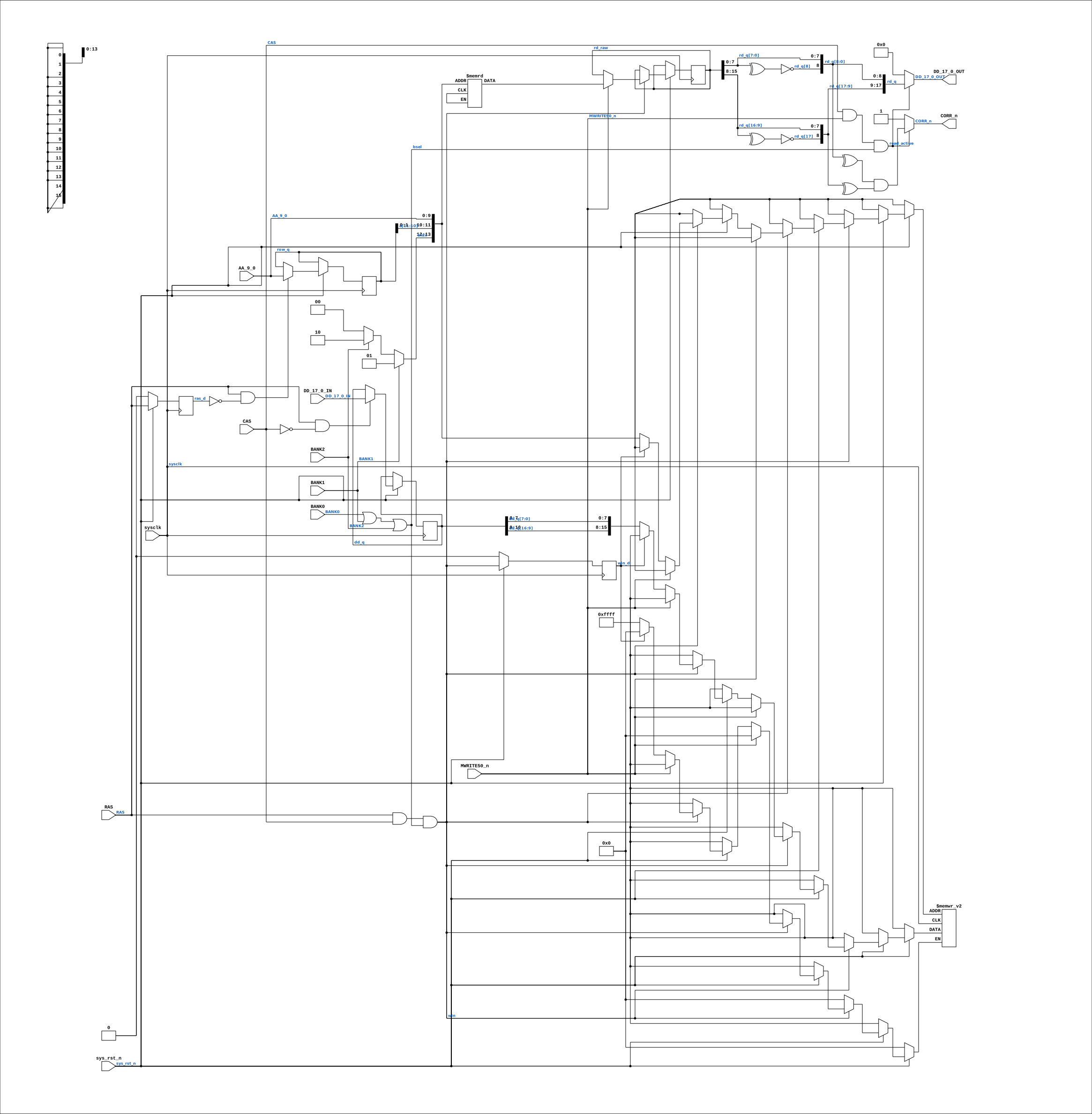
Schematic
Drawn from the Verilog: the yosys netlist of the Basys3 build, instance CORE.CPU_BOARD.MEM.RAM. Sub-modules are boxes (click the picture to open it full size; there every sub-module box links to its page, and every wire shows its Verilog name).
Description
ND120 CPU, MM&M MEM/RAM - block-RAM backend (any FPGA) Drop-in replacement for the sheet-49 RAM (MEM_RAM_49): one clean synchronous BRAM instead of six emulated SIP1M9 DRAM chips. Selected with `define MAIN_RAM_BLOCKRAM (see MEM_43.v). Implements the MEASURED DRAM protocol (docs/nd120-dram-memory.md section 4) with the hardware lessons of 8-JUL-2026 baked in: - row captured at the RAS rising edge (not level) - write data captured BEFORE CAS (the D bus is driven early and released around CAS-fall on silicon) - write executed ONCE, at the first RAS&CAS edge - registered read, held while CAS is active, bank-gated output Capacity: NUM_BANKS x 2^BANK_ADDR_BITS 18-bit words. Default 3 banks x 4K words = 24 KB (Basys3 xc7a35t BRAM budget). Boards with more BRAM raise BANK_ADDR_BITS (Nexys 4 DDR: ND120_BLOCKRAM_ADDR_BITS=15 in fpga/nexys4ddr/build.tcl). Linear word address = {row, col}: the row captured at RAS is the HIGH CPU address half (PAL 44902A drives HIEN during RAS, LOEN during CAS), so lin[BANK_ADDR_BITS-1:0] keeps the CONTIGUOUS low CPU address bits - addresses inside a bank slot are alias-free. Last reviewed: 8-JUL-2026 Ronny Hansen
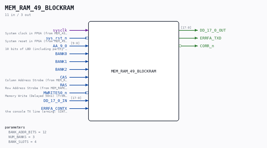
Parameters
| Parameter | Default |
|---|---|
BANK_ADDR_BITS |
12 |
NUM_BANKS |
3 |
BANK_SLOTS |
4 |
Ports
| Direction | Width | Name | Description |
|---|---|---|---|
| input | 1 |
sysclk |
System clock in FPGA (from MEM_43.sysclk) |
| input | 1 |
sys_rst_n (active low) |
System reset in FPGA (from MEM_43.sys_rst_n) |
| input | [9:0] |
AA_9_0 |
10 bits of LBD (including parity in bit 10)- 10 bit input to MEM/RAM (from MEM_ADDR_44.AA_9_0) |
| input | 1 |
BANK0 |
|
| input | 1 |
BANK1 |
|
| input | 1 |
BANK2 |
|
| input | 1 |
CAS |
Column Address Strobe (from MEM_RAMC_50.CAS) |
| input | 1 |
RAS |
Row Address Strobe (from MEM_RAMC_50.RAS) |
| input | 1 |
MWRITE50_n (active low) |
Memory Write (Delayed 50ns) (from MEM_LBDIF_48.MWRITE50_n) |
| input | [17:0] |
DD_17_0_IN |
|
| output | [17:0] |
DD_17_0_OUT |
|
| input | 1 |
ERRFA_CONTX |
the console TX line (arming: SINTRAN prints ERRFA) |
| output | 1 |
ERRFA_TXD |
|
| output | 1 |
CORR_n (active low) |
Verilog source
Verilog/CPU-BOARD-3202/circuit/MEM_RAM_49_BLOCKRAM.v on GitHub.
Show the Verilog of MEM_RAM_49_BLOCKRAM (489 lines)
/**************************************************************************
** ND120 CPU, MM&M                                                       **
** MEM/RAM - block-RAM backend (any FPGA)                                **
** Drop-in replacement for the sheet-49 RAM (MEM_RAM_49): one clean      **
** synchronous BRAM instead of six emulated SIP1M9 DRAM chips.           **
** Selected with `define MAIN_RAM_BLOCKRAM (see MEM_43.v).               **
**                                                                       **
** Implements the MEASURED DRAM protocol (docs/nd120-dram-memory.md      **
** section 4) with the hardware lessons of 8-JUL-2026 baked in:          **
**   - row captured at the RAS rising edge (not level)                   **
**   - write data captured BEFORE CAS (the D bus is driven early and     **
**     released around CAS-fall on silicon)                              **
**   - write executed ONCE, at the first RAS&CAS edge                    **
**   - registered read, held while CAS is active, bank-gated output      **
**                                                                       **
** Capacity: NUM_BANKS x 2^BANK_ADDR_BITS 18-bit words. Default 3 banks  **
** x 4K words = 24 KB (Basys3 xc7a35t BRAM budget). Boards with more     **
** BRAM raise BANK_ADDR_BITS (Nexys 4 DDR: ND120_BLOCKRAM_ADDR_BITS=15   **
** in fpga/nexys4ddr/build.tcl). Linear word address = {row, col}: the   **
** row captured at RAS is the HIGH CPU address half (PAL 44902A drives   **
** HIEN during RAS, LOEN during CAS), so lin[BANK_ADDR_BITS-1:0] keeps   **
** the CONTIGUOUS low CPU address bits - addresses inside a bank slot    **
** are alias-free.                                                       **
**                                                                       **
** Last reviewed: 8-JUL-2026                                             **
** Ronny Hansen                                                          **
***************************************************************************/

module MEM_RAM_49_BLOCKRAM #(
    parameter integer BANK_ADDR_BITS = 12,  // words per bank = 2**BANK_ADDR_BITS
    parameter integer NUM_BANKS = 3,        // informational; storage is BANK_SLOTS bank slots
    // Bank slots the array is DECLARED with. bidx (below) is only ever 0, 1 or
    // 2, so slot 3 can never be addressed: 4 slots waste a quarter of the
    // array (on the MiSTer ~64 M10K, and it turned a 64K-word bank into "does
    // not fit"), while 3 slots hold exactly the three banks. 4 stays the
    // default so every proven build (Nexys, Basys3) is unchanged; the MiSTer
    // sets 3 through ND120_BLOCKRAM_BANK_SLOTS (MEM_43.v). Either value is
    // covered by test-blockram-space / test-blockram-space-3banks.
    parameter integer BANK_SLOTS = 4
) (
    // Input signals (sheet-49 interface, same as MEM_RAM_49)
    input sysclk,        //! System clock in FPGA (from MEM_43.sysclk)
    input sys_rst_n,     //! System reset in FPGA (from MEM_43.sys_rst_n)

    input [9:0] AA_9_0,  //! 10 bits of LBD (including parity in bit 10)- 10 bit input to MEM/RAM (from MEM_ADDR_44.AA_9_0)
    input       BANK0,
    input       BANK1,
    input       BANK2,

    input CAS,           //! Column Address Strobe (from MEM_RAMC_50.CAS)
    input RAS,           //! Row Address Strobe (from MEM_RAMC_50.RAS)

    input MWRITE50_n,    //! Memory Write (Delayed 50ns) (from MEM_LBDIF_48.MWRITE50_n)

    input  [17:0] DD_17_0_IN,
    output [17:0] DD_17_0_OUT,

`ifdef ND120_ERRFA_PROBE
    input  ERRFA_CONTX,  // the console TX line (arming: SINTRAN prints ERRFA)
    output ERRFA_TXD,
`endif

    output CORR_n
);

  /* verilator lint_off UNUSEDSIGNAL */
  wire [31:0] unused_params = NUM_BANKS;
  /* verilator lint_on UNUSEDSIGNAL */

  // {high byte, low byte} -> full 18-bit word with regenerated odd parity
  function [17:0] with_parity(input [15:0] d);
    with_parity = {~(^d[15:8]), d[15:8], ~(^d[7:0]), d[7:0]};
  endfunction

  reg [9:0] row_q;
  reg       ras_d;
  reg [17:0] dd_q;    // write data captured while RAS active, CAS not yet seen
  reg        win_d;   // access window (RAS & CAS & bank), one sysclk delayed

`ifdef QUARTUS_RAM_INFER
  // Quartus arm (01-SEP-2026) - plain Verilog, for the reasons set out in
  // Shared/support/IDT6168A_20.v (Quartus 17.0.2 refused to infer M10K from
  // the reference arm: "Cannot convert all sets of registers into RAM
  // megafunctions", the register fallback overflows the device). An explicit
  // altsyncram megafunction arm came first (31-AUG-2026) and was deleted
  // 01-SEP-2026 once this arm had booted the board; its history, and the
  // two-clock read it shipped with, are recorded in IDT6168A_20.v. One
  // lesson from it is kept here: with read_during_write_mode "DONT_CARE" and
  // rden_a tied high, rd_raw was UNDEFINED on every write cycle where the
  // reference holds - only this board compiled that arm, so the simulator
  // could never show the difference. Same array below, same 1-clock
  // registered read, same hold-while-writing.
  //
  // Two differences from the reference arm below, both aimed at inference:
  //
  //  1. The array read and write live in their OWN always block, NOT inside
  //     the sys_rst_n branch of the main one. A memory write sitting under a
  //     reset condition is a well-known inference blocker, and there is no
  //     reason for it here - the array is never reset, only ras_d/win_d are.
  //
  //  2. The read is unconditional apart from its enable. Where the reference
  //     holds rd_raw through a write, this re-reads and discards - which is
  //     what ramstyle "no_rw_check" declares. rd_raw is only ever SAMPLED
  //     during a read window (win && MWRITE50_n), so what it carries during
  //     a write window is not observable.
  //
  // Build v47 (01-SEP-2026) inferred this array as M10K (405/553 M10K used,
  // one uninferred RAM left on the device and it is not this one).
  (* ramstyle = "no_rw_check, M10K" *)
  reg [15:0] mem[0:(BANK_SLOTS << BANK_ADDR_BITS)-1];

  reg [15:0] rd_raw;
  wire [17:0] rd_q = with_parity(rd_raw);

  always @(posedge sysclk) begin
    if (win) begin
      rd_raw <= mem[{bidx, a}];
      // write: ONCE, on the first window edge - same condition as the
      // reference arm
      if (!MWRITE50_n && !win_d) mem[{bidx, a}] <= {dd_q[16:9], dd_q[7:0]};
    end
  end
`else
  // One 16-bit wide BRAM, BANK_SLOTS bank slots (slot 3, when declared,
  // is unreachable - see the parameter).
  // PARITY IS NEVER STORED (policy, Ronny 3-AUG-2026): the two parity bits
  // DD[8] and DD[17] are dropped on write and regenerated as ODD parity on
  // read, exactly as MEM_RAM_49_SDRAM and SIP1M9 do. 18 bits wide would have
  // cost extra block RAM to hold bits nothing reads back.
  // cascade_height = 1: at BANK_ADDR_BITS=15 the 128K-word array otherwise
  // infers CASCADED RAMB36 pairs, and Vivado's DRC REQP-1962 (cascade ADDR15
  // tie-off check) rejects the inferred netlist at place_design (measured
  // 22-AUG-2026, Nexys clk=12 build). Standalone RAMB36 + LUT decode passes.
  // ramstyle is QUARTUS's spelling - see the note in Shared/support/IDT6168A_20.v.
  (* ram_style = "block", cascade_height = 1, syn_ramstyle = "block_ram", ramstyle = "M10K" *)
  reg [15:0] mem[0:(BANK_SLOTS << BANK_ADDR_BITS)-1];

  // Raw registered array read. The parity regeneration must sit AFTER this
  // register: with_parity() between the array and the register put an XOR
  // function in the read path, which stopped Vivado inferring block RAM -
  // the whole 16K x 16 array fell back to 1024 RAM256X1S distributed-RAM
  // primitives (measured 21-AUG-2026, Synth 8-6849). Registered raw read =
  // BRAM-mappable; the parity bits are combinational on the FF output.
  reg [15:0] rd_raw;
  wire [17:0] rd_q = with_parity(rd_raw);
`endif

  // Linear word address {row, col}. PAL 44902A (sheet 50) drives HIEN_n
  // during the RAS phase and LOEN_n during the CAS phase, so the ROW
  // captured at the RAS edge is the HIGH address half (CPU addr[19:10])
  // and AA during the window carries the LOW half (CPU addr[9:0]) - the
  // same order the silicon-proven Tang bridge uses (MEM_RAM_49_SDRAM.v
  // s_addr = {bank, row_q, AA_9_0}). The 22-AUG-2026 Nexys 400& fault was
  // this concatenation REVERSED: lin[11:0] then kept only {addr[1:0],
  // addr[19:10]} and CPU address bits [9:2] never reached the BRAM
  // (proven by OPCOM deposit aliasing 1000<->1004<->...<->0).
  wire [19:0] lin = {row_q, AA_9_0};
  wire [BANK_ADDR_BITS-1:0] a = lin[BANK_ADDR_BITS-1:0];
  wire [1:0] bidx = BANK1 ? 2'd1 : (BANK2 ? 2'd2 : 2'd0);
  wire bsel = BANK0 | BANK1 | BANK2;
  wire win = RAS & CAS & bsel;

`ifdef ND120_ILA_MARK_DEBUG
  // Nexys build.tcl -tclargs ila: named copies of the write port for the
  // JTAG ILA (LIST-FILE-NAMES corruption-writer hunt, 24-AUG). The write
  // fires on the first win edge with MWRITE50_n low - s_ila_ram_wr is that
  // exact condition, s_ila_ram_addr/wdata the address and data it uses.
  // No functional effect; the define is set only by that build flag.
  (* mark_debug = "true" *) wire [BANK_ADDR_BITS-1:0] s_ila_ram_addr = a;
  (* mark_debug = "true" *) wire s_ila_ram_wr = win & ~win_d & ~MWRITE50_n;
  (* mark_debug = "true" *) wire [15:0] s_ila_ram_wdata = {dd_q[16:9], dd_q[7:0]};
`endif

  always @(posedge sysclk) begin
    if (!sys_rst_n) begin
      ras_d <= 0;
      win_d <= 0;
    end else begin
      ras_d <= RAS;
      win_d <= win;

      // row: exactly once, at the RAS rising edge (AA carries the row there)
      if (RAS && !ras_d) row_q <= AA_9_0;

      // write data: capture every edge until CAS is seen high - the final
      // capture (the CAS-fall edge) holds the settled pre-CAS value
      if (RAS && !CAS) dd_q <= DD_17_0_IN;

`ifndef QUARTUS_RAM_INFER
      // The Quartus arm takes this read/write elsewhere, in its own always
      // block. See the mem/rd_raw declarations above. Note the array write
      // below sits inside the sys_rst_n else-branch, which is one of the
      // things the inference arm deliberately moves out.
      if (win) begin
        if (MWRITE50_n) begin
          // read: registered raw, re-reads while CAS; parity regenerated
          // combinationally AFTER the register (see rd_raw above)
          rd_raw <= mem[{bidx, a}];
        end else if (!win_d) begin
          // write: ONCE, first window edge; the two parity bits are dropped
          mem[{bidx, a}] <= {dd_q[16:9], dd_q[7:0]};
        end
      end
`endif
    end
  end

`ifdef ND120_ERRFA_PROBE
  // SINTRAN ERRFATAL evidence probe (24-AUG-2026). SINTRAN's ERRFA routine
  // (0o004356 in the M06 resident) saves X,T,A,D,L to words 0o4347-0o4353
  // of bank 0 BEFORE printing "Sintran halt in ERRFATAL" and halting. On
  // the crash the CPU never drops to STOP (OPCOM unreachable) and no JTAG
  // ILA fits beside the addr16 main RAM (270/270 RAMB18 sites), so this
  // latches those five write values into flip-flops and, once the L save
  // has been seen and ~2 s passed, repeats them forever as one octal line
  //   EF <X> <T> <A> <D> <L> <SVLCA> <SVLWC> <SSTAT> <9TREG> <9XREG>
  // on its own 9600-baud TX line, which the board top wire-ANDs onto the
  // console TX (idle high; SINTRAN is halted, the console is free).
  // T decodes the failing Winchester-driver check: 0=HDERR 1=MORER
  // 4=MEMER 10=LAOUR 100=DILLC 200=CNACT (23-WINCHESTER-POF.NPL DERR).
  // Zero block RAM, no functional effect; define set by build.tcl
  // -tclargs errfaprobe only.
  // Bit clock and arming gap, define-overridable so the unit bench
  // (sim/MEM_RAM_49_BLOCKRAM_ERRFA_tb.v) can run in sim time.
`ifndef ND120_ERRFA_BAUD_DIV
  `define ND120_ERRFA_BAUD_DIV 1736
`endif
`ifndef ND120_ERRFA_GAP_BITS
  `define ND120_ERRFA_GAP_BITS 25
`endif
`ifndef ND120_ERRFA_RWAIT_BITS
  `define ND120_ERRFA_RWAIT_BITS 23
`endif
  localparam integer EFP_BAUD_DIV = `ND120_ERRFA_BAUD_DIV;  // clk / 9600
  localparam integer EFP_GAP_BITS = `ND120_ERRFA_GAP_BITS;  // ~2 s arming gap
  localparam integer EFP_RWAIT_BITS = `ND120_ERRFA_RWAIT_BITS;  // ~0.5 s to the P line

  reg [15:0] efp_cap[0:9];
  reg        efp_armed;
  reg [EFP_GAP_BITS-1:0] efp_gap;  // inter-line pacing / initial ~2 s delay
  reg [ 6:0] efp_char;     // 0..74 within the line
  reg [ 3:0] efp_bit;      // 10 bits per char
  reg [11:0] efp_baud;
  reg        efp_txd;
  reg        efp_sending;

  wire efp_wr = win & ~win_d & ~MWRITE50_n & BANK0;
  wire [15:0] efp_wdata = {dd_q[16:9], dd_q[7:0]};
  wire [15:0] efp_a16 = {{(16 - BANK_ADDR_BITS) {1'b0}}, a};

  // ARMING (third design, 24-AUG). The first trigger ("L cell written")
  // armed during the bulk resident load - in octal 4347..4353 are
  // consecutive, so a memory sweep writes the same five cells in the same
  // order. The second ("five writes in strict order, not preceded by the
  // 4346 neighbor") never armed on silicon - the real microcode's write
  // pattern around ERRFA's saves is not the clean ascending burst the
  // bench modeled. This design assumes NOTHING about write order:
  //   * the five capture registers always track the LAST value written to
  //     their cell (bulk loads just update them harmlessly);
  //   * arming watches the CONSOLE TX line for SINTRAN's own crash text -
  //     a 9600-baud deserializer on ERRFA_CONTX matches the ASCII
  //     sequence "ERRFA". Only a machine that is announcing the crash can
  //     arm the probe, so the live console is never garbled.
  // console-TX "ERRFA" matcher state
  reg [11:0] efp_rxbaud;
  reg [ 3:0] efp_rxbit;   // 0 = hunting start bit
  reg [ 7:0] efp_rxsh;
  reg [39:0] efp_txt;     // last five received chars

  // ---- READ-HISTORY RING (the "P" line) --------------------------------
  // 128-entry LUTRAM ring of the last RAM READ addresses before the fatal
  // ERRFA entry. Freeze rule: a read of 0o4356 (ERRFA's first word) whose
  // PREVIOUS read was not the sequential neighbor 0o4355 = a JUMP into
  // ERRFA (the fatal call). Sequential sweeps (SINTRAN's memory scrub
  // reads 4355 then 4356) never freeze it; nothing else reads 4356.
  // At freeze the ring holds the last ~128 reads of the dying path -
  // WISTA's final instructions, the caller, and the operand read that
  // delivered the illegal function code. Printed ONCE as
  //   P aaaaaa aaaaaa ... (oldest first, 128 entries)
  // starting ~0.5 s after the console matcher arms - after SINTRAN's
  // crash text has flushed, before the first EF line at ~2 s.
  reg [15:0] efp_ring[0:127];
  reg [ 6:0] efp_rwp;
  reg        efp_frozen;
  reg [15:0] efp_prev_rd;
  reg        efp_rdump;     // ring dump done
  reg        efp_rsend;     // ring dump in progress
  reg [EFP_RWAIT_BITS-1:0] efp_rwait;  // delay from arming to the ring line
  reg [ 9:0] efp_rchar;     // 0..898: "P " + 128*7 chars + CR LF
  reg [ 3:0] efp_rbit;
  reg [11:0] efp_rbaud;
  reg        efp_rtxd;
  reg [15:0] efp_rword;
  wire efp_rd = win & ~win_d & MWRITE50_n & bsel;

  // one line = 40 chars: "EF " + five "dddddd " groups (last group's
  // trailing slot pair = CR LF)
  function [7:0] efp_octdig(input [15:0] w, input [2:0] d);
    case (d)
      3'd0: efp_octdig = 8'h30 + {7'b0, w[15]};
      3'd1: efp_octdig = 8'h30 + {5'b0, w[14:12]};
      3'd2: efp_octdig = 8'h30 + {5'b0, w[11:9]};
      3'd3: efp_octdig = 8'h30 + {5'b0, w[8:6]};
      3'd4: efp_octdig = 8'h30 + {5'b0, w[5:3]};
      default: efp_octdig = 8'h30 + {5'b0, w[2:0]};
    endcase
  endfunction

  // ring line character mux: "P " + 128 x "dddddd " + CR LF = 900 chars
  wire [9:0] efp_rrel = efp_rchar - 10'd2;
  wire [9:0] efp_rg10 = efp_rrel / 10'd7;
  wire [9:0] efp_rd10 = efp_rrel % 10'd7;
  wire [6:0] efp_rg   = efp_rg10[6:0];
  wire [3:0] efp_rd7  = efp_rd10[3:0];
  wire [6:0]  efp_ridx = efp_rwp + efp_rg;           // explicit 7-bit wrap
  wire [15:0] efp_rw  = efp_ring[efp_ridx];          // oldest-first
  reg [7:0] efp_rch;
  always @(*) begin
    if (efp_rchar == 10'd0) efp_rch = "P";
    else if (efp_rchar == 10'd1) efp_rch = " ";
    else if (efp_rchar == 10'd898) efp_rch = 8'h0D;
    else if (efp_rchar == 10'd899) efp_rch = 8'h0A;
    else if (efp_rd7 == 4'd6) efp_rch = " ";
    else efp_rch = efp_octdig(efp_rw, efp_rd7[2:0]);
  end

  wire [6:0] efp_rel = efp_char - 7'd3;  // 0..69 inside the digit groups
  wire [6:0] efp_w6  = efp_rel / 7'd7;   // word index 0..9
  wire [6:0] efp_d6  = efp_rel % 7'd7;   // digit 0..5, 6 = separator space

  reg [7:0] efp_ch;
  always @(*) begin
    if (efp_char == 7'd0) efp_ch = "E";
    else if (efp_char == 7'd1) efp_ch = "F";
    else if (efp_char == 7'd2) efp_ch = " ";
    else if (efp_char == 7'd73) efp_ch = 8'h0D;
    else if (efp_char == 7'd74) efp_ch = 8'h0A;
    else if (efp_d6 == 7'd6) efp_ch = " ";
    else efp_ch = efp_octdig(efp_cap[efp_w6[3:0]], efp_d6[2:0]);
  end

  always @(posedge sysclk) begin
    if (!sys_rst_n) begin
      efp_armed   <= 1'b0;
      efp_gap     <= {EFP_GAP_BITS{1'b0}};
      efp_char    <= 7'd0;
      efp_bit     <= 4'd0;
      efp_baud    <= 12'd0;
      efp_txd     <= 1'b1;
      efp_sending <= 1'b0;
      efp_rxbaud <= 12'd0;
      efp_rxbit  <= 4'd0;
      efp_rxsh   <= 8'd0;
      efp_txt    <= 40'd0;
      efp_rwp    <= 7'd0;
      efp_frozen <= 1'b0;
      efp_prev_rd <= 16'hFFFF;
      efp_rdump  <= 1'b0;
      efp_rsend  <= 1'b0;
      efp_rwait  <= {EFP_RWAIT_BITS{1'b0}};
      efp_rchar  <= 10'd0;
      efp_rbit   <= 4'd0;
      efp_rbaud  <= 12'd0;
      efp_rtxd   <= 1'b1;
    end else begin
      // read-history ring: record every RAM read until the jump into ERRFA
      if (efp_rd) begin
        efp_prev_rd <= efp_a16;
        if (!efp_frozen) begin
          efp_ring[efp_rwp] <= efp_a16;
          efp_rwp <= efp_rwp + 7'd1;
          if (efp_a16 == 16'o4356 && efp_prev_rd != 16'o4355)
            efp_frozen <= 1'b1;                  // the fatal call - stop here
        end
      end

      // ring dump: once, ~0.5 s after the console matcher arms (after the
      // crash text, before the first EF line at ~2 s)
      if (efp_armed && efp_frozen && !efp_rdump && !efp_rsend) begin
        efp_rwait <= efp_rwait + 1'b1;
        if (&efp_rwait) begin
          efp_rsend <= 1'b1;
          efp_rchar <= 10'd0;
          efp_rbit  <= 4'd0;
          efp_rbaud <= 12'd0;
        end
      end
      if (efp_rsend) begin
        if (efp_rbaud == EFP_BAUD_DIV[11:0] - 12'd1) begin
          efp_rbaud <= 12'd0;
          if (efp_rbit == 4'd9) begin
            efp_rbit <= 4'd0;
            efp_rtxd <= 1'b1;
            if (efp_rchar == 10'd899) begin
              efp_rsend <= 1'b0;
              efp_rdump <= 1'b1;                 // once only
            end else efp_rchar <= efp_rchar + 10'd1;
          end else begin
            efp_rbit <= efp_rbit + 4'd1;
            if (efp_rbit == 4'd0) efp_rtxd <= 1'b0;
            else if (efp_rbit <= 4'd8) efp_rtxd <= efp_rch[efp_rbit-1];
            else efp_rtxd <= 1'b1;
          end
        end else efp_rbaud <= efp_rbaud + 12'd1;
      end

      // capture: always track the last write into each save cell
      if (efp_wr) begin
        case (efp_a16)
          16'o4347: efp_cap[0] <= efp_wdata;
          16'o4350: efp_cap[1] <= efp_wdata;
          16'o4351: efp_cap[2] <= efp_wdata;
          16'o4352: efp_cap[3] <= efp_wdata;
          16'o4353: efp_cap[4] <= efp_wdata;
          // the Winchester driver datafield (B=042346): issue-time values
          // of the FAILING transfer - SVLCA (expected low address), SVLWC
          // (word count), SSTAT (last hardware status WISTA saw)
          16'o42312: efp_cap[5] <= efp_wdata;
          16'o42313: efp_cap[6] <= efp_wdata;
          16'o42244: efp_cap[7] <= efp_wdata;
          // WISTA's entry save of the caller's T,A,D / X (TAD=:SATAD at
          // B-32 / X at B-27): cap[8] = 9TREG = the FUNCTION argument the
          // driver was handed, cap[9] = 9XREG.
          16'o42314: efp_cap[8] <= efp_wdata;
          16'o42317: efp_cap[9] <= efp_wdata;
          default: ;
        endcase
      end

      // arming: deserialize the console TX (8N1) and match "ERRFA"
      if (efp_rxbit == 4'd0) begin
        if (!ERRFA_CONTX) begin                  // start bit edge
          efp_rxbit  <= 4'd1;
          efp_rxbaud <= EFP_BAUD_DIV[11:0] + EFP_BAUD_DIV[11:0] / 12'd2 - 12'd1;
        end
      end else if (efp_rxbaud != 12'd0) begin
        efp_rxbaud <= efp_rxbaud - 12'd1;
      end else if (efp_rxbit <= 4'd8) begin      // data bits, LSB first
        efp_rxsh   <= {ERRFA_CONTX, efp_rxsh[7:1]};
        efp_rxbit  <= efp_rxbit + 4'd1;
        efp_rxbaud <= EFP_BAUD_DIV[11:0] - 12'd1;
      end else begin                             // stop-bit slot: char done
        efp_rxbit <= 4'd0;
        efp_txt   <= {efp_txt[31:0], efp_rxsh};
        if ({efp_txt[31:0], efp_rxsh} == {"E", "R", "R", "F", "A"})
          efp_armed <= 1'b1;
      end
      if (efp_armed && !efp_sending) begin
        efp_gap <= efp_gap + 1'b1;
        if (&efp_gap) begin                      // ~2 s after arming
          efp_sending <= 1'b1;
          efp_char    <= 7'd0;
          efp_bit     <= 4'd0;
          efp_baud    <= 12'd0;
        end
      end
      if (efp_sending) begin
        if (efp_baud == EFP_BAUD_DIV[11:0] - 12'd1) begin
          efp_baud <= 12'd0;
          if (efp_bit == 4'd9) begin
            efp_bit <= 4'd0;
            efp_txd <= 1'b1;
            if (efp_char == 7'd74) begin
              efp_sending <= 1'b0;               // line done; gap restarts
              efp_gap     <= {EFP_GAP_BITS{1'b0}};
            end else efp_char <= efp_char + 7'd1;
          end else begin
            efp_bit <= efp_bit + 4'd1;
            if (efp_bit == 4'd0) efp_txd <= 1'b0;               // start bit
            else if (efp_bit <= 4'd8) efp_txd <= efp_ch[efp_bit-1];
            else efp_txd <= 1'b1;                               // stop
          end
        end else efp_baud <= efp_baud + 12'd1;
      end
    end
  end

  assign ERRFA_TXD = efp_txd & efp_rtxd;
`endif

  // Output gating: same convention as the chips (0 when not selected/reading)
  wire read_active = CAS & MWRITE50_n & bsel;
  assign DD_17_0_OUT = read_active ? rd_q : 18'b0;

  // Parity check outputs, same formula as two SIP1M9 chips (low = DD[8:0],
  // high = DD[17:9]), AND-combined; 1 when inactive
  assign CORR_n = read_active ? ((^rd_q[8:0]) & (^rd_q[17:9])) : 1'b1;

endmodule