CPU_CS_TCV_20
Source: Verilog/CPU-BOARD-3202/circuit/CPU_CS_TCV_20.v
Where it sits (Simulation): ND120_TOP > ND120_CORE > ND3202D > CPU_15 > CPU_CS_16 > CPU_CS_TCV_20
- instance path: CORE.CPU_BOARD.CPU.CS.TCV
Used in: CPU_CS_16 (all tops)
Contains: no other modules.
Module hierarchy - All modules
Schematic
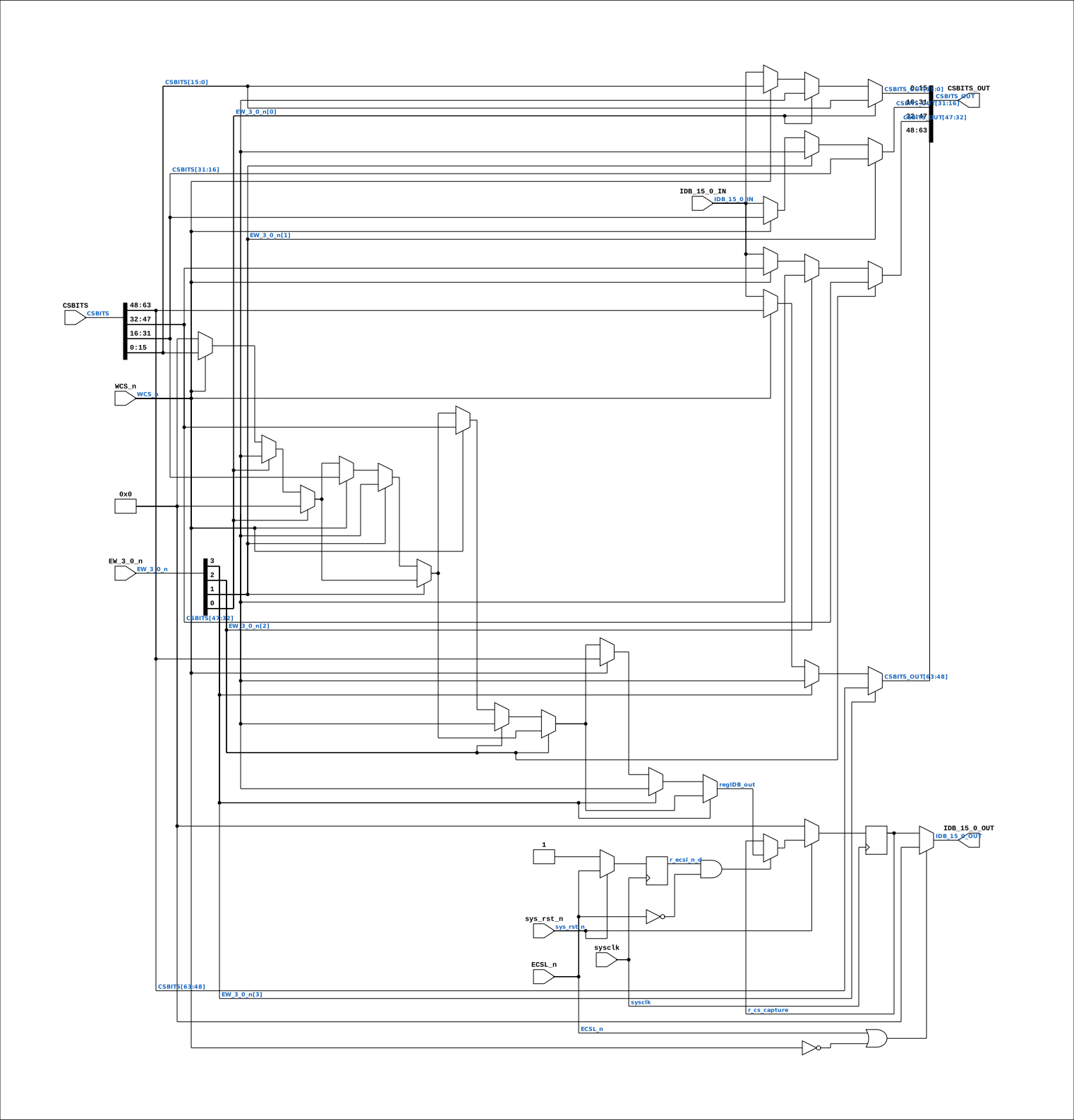
Drawn from the Verilog: the yosys netlist of the Simulation (Verilator) build, instance CORE.CPU_BOARD.CPU.CS.TCV. Sub-modules are boxes (click the picture to open it full size; there every sub-module box links to its page, and every wire shows its Verilog name).
Description
ND120 CPU, MM&M CPU/CS/TCV CS TRANSCEIVERS SHEET 20 of 50 Last reviewed: 14-APRIL-2024 Ronny Hansen
Ports
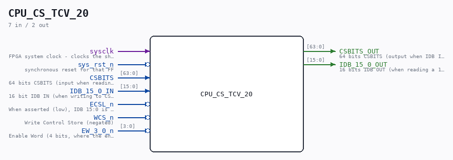
| Direction | Width | Name | Description |
|---|---|---|---|
| input | 1 |
sysclk |
FPGA system clock - clocks the sheet-20 CS capture FF |
| input | 1 |
sys_rst_n (active low) |
synchronous reset for that FF |
| input | [63:0] |
CSBITS |
64 bits CSBITS (input when reading from CSBITS to IDB OUT) |
| output | [63:0] |
CSBITS_OUT |
64 bits CSBITS (output when IDB IN writes a 16 bit part to the CSBITS) |
| input | [15:0] |
IDB_15_0_IN |
16 bit IDB IN (when writing to CSBITS) |
| output | [15:0] |
IDB_15_0_OUT |
16 bits IDB OUT (when reading a 16 bit word from CSBITS) |
| input | 1 |
ECSL_n (active low) |
When asserted (low), IDB 15:0 is connected to IDB 15:0. Source PAL_44305D, CPU_CS_CTL_18. Comment in the PAL source says "ECSL HOLD IN g AND h cycles" |
| input | 1 |
WCS_n (active low) |
Write Control Store (negated) |
| input | [3:0] |
EW_3_0_n (active low) |
Enable Word (4 bits, where the enabled word (0-3) has its bit set to 0. Chooses which 16 bits of the 64 bits CSBITS that is read or written |
Verilog source
Verilog/CPU-BOARD-3202/circuit/CPU_CS_TCV_20.v on GitHub.
Show the Verilog of CPU_CS_TCV_20 (157 lines)
/**************************************************************************
** ND120 CPU, MM&M                                                       **
** CPU/CS/TCV                                                            **
** CS TRANSCEIVERS                                                       **
** SHEET 20 of 50                                                        **
**                                                                       **
** Last reviewed: 14-APRIL-2024                                          **
** Ronny Hansen                                                          **
***************************************************************************/

module CPU_CS_TCV_20 (
    input        sysclk,     //! FPGA system clock - clocks the sheet-20 CS capture FF
    input        sys_rst_n,  //! synchronous reset for that FF
    input [63:0] CSBITS,  //! 64 bits CSBITS (input when reading from CSBITS to IDB OUT)
    output [63:0] CSBITS_OUT,     //! 64 bits CSBITS (output when IDB IN writes a 16 bit part to the CSBITS)

    input  [15:0] IDB_15_0_IN,  //! 16 bit IDB IN (when writing to CSBITS)
    output [15:0] IDB_15_0_OUT, //! 16 bits IDB OUT (when reading a 16 bit word from CSBITS)

    input ECSL_n,                 //! When asserted (low), IDB 15:0 is connected to IDB 15:0. Source PAL_44305D, CPU_CS_CTL_18. Comment in the PAL source says "ECSL HOLD IN g AND h cycles"
    input WCS_n,  //! Write Control Store (negated)
    input [3:0] EW_3_0_n          //! Enable Word (4 bits, where the enabled word (0-3) has its bit set to 0. Chooses which 16 bits of the 64 bits CSBITS that is read or written
);


  /*******************************************************************************
   ** The wires are defined here                                                 **
   *******************************************************************************/
  reg [63:0] regCSBITS;
  reg [15:0] regIDB_out;


  // WCS_n decides is its DIR-ection of the data from CSBITS => IDB or CSBITS <= IDB
  wire DIR;  //  DIR = H (A to B - CSBITS to IDB)  or DIR = L (B to A - IDB to CSBITS)
  assign DIR = WCS_n;

  // Fixed: Initialize all signals to prevent latch inference
  always @(*) begin

    regIDB_out = 16'b0;
    regCSBITS  = CSBITS;  // Default to pass-through input value

    if (EW_3_0_n[0] == 0) begin
      if (DIR) begin
        //regIDB_out = regIDB_out | CSBITS[15:0];
        regIDB_out = CSBITS[15:0];
      end else begin
        regCSBITS[15:0] = IDB_15_0_IN;
      end
    end

    if (EW_3_0_n[1] == 0) begin
      if (DIR) begin
        //regIDB_out = regIDB_out | CSBITS[31:16];
        regIDB_out = CSBITS[31:16];
      end else begin
        regCSBITS[31:16] = IDB_15_0_IN;
      end
    end

    if (EW_3_0_n[2] == 0) begin
      if (DIR) begin
        //regIDB_out = regIDB_out | CSBITS[47:32];
        regIDB_out = CSBITS[47:32];
      end else begin
        regCSBITS[47:32] = IDB_15_0_IN;
      end
    end

    if (EW_3_0_n[3] == 0) begin
      if (DIR) begin
        //regIDB_out = regIDB_out | CSBITS[63:48];
        regIDB_out = CSBITS[63:48];
      end else begin
        regCSBITS[63:48] = IDB_15_0_IN;
      end
    end

  end


  // Write to CSBITS from IDB
  //assign s_csbits_15_0  = (!WCS_n & !EW_3_0_n[0]) ? IDB_15_0_IN : CSBITS[15:0];
  //assign s_csbits_31_16 = (!WCS_n & !EW_3_0_n[1]) ? IDB_15_0_IN : CSBITS[31:16];
  //assign s_csbits_47_32 = (!WCS_n & !EW_3_0_n[2]) ? IDB_15_0_IN : CSBITS[47:32];
  //assign s_csbits_63_48 = (!WCS_n & !EW_3_0_n[3]) ? IDB_15_0_IN : CSBITS[63:48];


  // Write to IDB from CSBITS
  //assign regidb = EW_3_0_n[0] ? 16'b0 : CSBITS[15:0];
  //assign regidb = EW_3_0_n[1] ? 16'b0 : CSBITS[31:16];
  //assign regidb = EW_3_0_n[2] ? 16'b0 : CSBITS[47:32];
  //assign regidb = EW_3_0_n[3] ? 16'b0 : CSBITS[63:48];


  /*****************************************************************************
   ** THE CS OUTPUT CAPTURE (sheet 20, chips 8C and 9C)                        **
   **                                                                          **
   ** The drawing puts TWO 74PCT373 octal latches between the word-select       **
   ** '245s above and the IDB: 9C carries IDB15..IDB8, 8C carries IDB7..IDB0.   **
   ** On BOTH chips the SAME net - ECSL~ - drives pin 11 (C, latch enable) AND  **
   ** pin 1 (/OC, output control). That is the whole point:                     **
   **                                                                          **
   **   ECSL~ = 1 : C high  -> latch transparent, BUT /OC high -> outputs are   **
   **               tri-stated, so the tracking is not observable anywhere.     **
   **   ECSL~ = 0 : C low   -> latch HOLDS, and /OC low -> outputs drive IDB.   **
   **                                                                          **
   ** Because the transparent window never drives the bus, the only behaviour   **
   ** anything can see is: CAPTURE ON THE FALLING EDGE OF ECSL~, then hold that **
   ** value on the IDB for as long as ECSL~ stays low. That is an EDGE-         **
   ** TRIGGERED FLIP-FLOP, not a latch - so this is modelled with a plain       **
   ** posedge-sysclk edge detect. No transparent latch, nothing inferred.       **
   ** (Same reasoning as the AM29C821 conversion: a control signal used as a    **
   ** clock becomes an EDGE-DETECT, never a level.)                             **
   **                                                                          **
   ** WHY IT MATTERS (root cause of TRA CS returning 000000, 08-AUG-2026):      **
   ** this capture was missing entirely - ECSL_n was an unused input port and   **
   ** the read path was a straight combinational mux. During an RWCS microcycle **
   ** PAL_44305D asserts ECSL at cycle state 0101 while EWCA is still on, so    **
   ** LUA still holds the ADCS-latched control-store address and the correct    **
   ** word is on the '245 outputs - that edge is the capture. EWCA then drops   **
   ** at state 1100, MA and LUA move to the microaddress to be EXECUTED (which  **
   ** is what PAL_44307C's MCLK comment describes), the control store re-reads, **
   ** and without this flip-flop the word simply vanished. ECSL stays asserted  **
   ** through to TERM - PAL_44305D's own comments call the two terms "READ      **
   ** CONTROL STORE HOLD" and "HOLD OVERLAP WITH EWCA" - so the captured word   **
   ** is still on the IDB when ALUCLK writes the A register at TERM.            **
   *****************************************************************************/

  reg [15:0] r_cs_capture;
  reg        r_ecsl_n_d;

  always @(posedge sysclk) begin
    if (!sys_rst_n) begin
      r_cs_capture <= 16'b0;
      r_ecsl_n_d   <= 1'b1;
    end else begin
      r_ecsl_n_d <= ECSL_n;
      // falling edge of ECSL~ = the 373s closing = the capture instant
      if (r_ecsl_n_d && !ECSL_n) r_cs_capture <= regIDB_out[15:0];
    end
  end

  // ECSL_n decides if the data should be enabled out (on the IDB bus and the CSBITS output bus).
  // Inside the FPGA a disabled "3-state" driver must drive 0, never z.
  //assign IDB_15_0_OUT = (ECSL_n & !WCS_n) ? 16'b0 : regIDB[15:0];
  assign IDB_15_0_OUT = (ECSL_n | !WCS_n) ? 16'b0 : r_cs_capture;

  //assign CSBITS_OUT[63:0] = (ECSL_n & WCS_n) ? 64'b0 : regCSBITS[63:0];
  //assign CSBITS_OUT[63:0] = (WCS_n) ? 64'b0 : regCSBITS[63:0];
  assign CSBITS_OUT[63:0] = regCSBITS;


endmodule