IO_PANCAL_40
Source: Verilog/CPU-BOARD-3202/circuit/IO_PANCAL_40.v
Where it sits (Simulation): ND120_TOP > ND120_CORE > ND3202D > IO_37 > IO_PANCAL_40
- instance path: CORE.CPU_BOARD.IO.PANCAL
Used in: IO_37 (all tops)
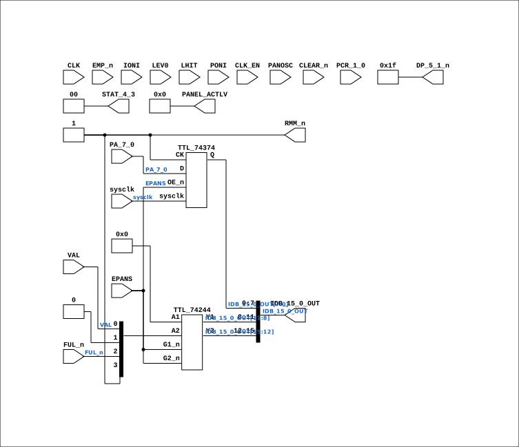
Contains: PANCAL_68705_CLOCK (only on Nexys, MiSTer, MEGA65 R6, MEGA65 R3, QMTECH), TTL_74244, TTL_74374
Module hierarchy - All modules
Schematic
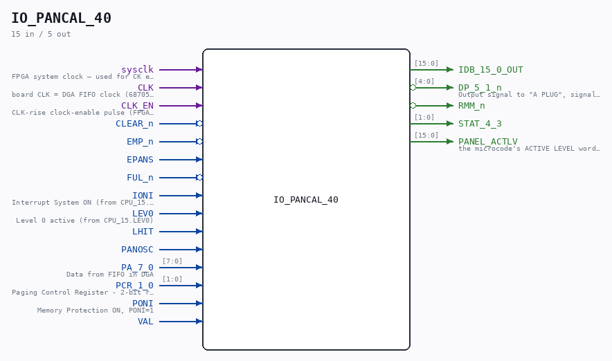
Drawn from the Verilog: the yosys netlist of the Simulation (Verilator) build, instance CORE.CPU_BOARD.IO.PANCAL. Sub-modules are boxes (click the picture to open it full size; there every sub-module box links to its page, and every wire shows its Verilog name).
Description
ND120 CPU, MM&M IO/PANCAL PANEL PROC & CALENDAR SHEET 40 of 50 Last reviewed: 2-FEB-2025 Ronny Hansen
Ports
| Direction | Width | Name | Description |
|---|---|---|---|
| input | 1 |
sysclk |
FPGA system clock — used for CK edge detection in CHIP_32B |
| input | 1 |
CLK |
board CLK = DGA FIFO clock (68705 emulation, latch mode) |
| input | 1 |
CLK_EN |
CLK-rise clock-enable pulse (FPGA_FF_MODE, else 0) |
| input | 1 |
CLEAR_n (active low) |
|
| input | 1 |
EMP_n (active low) |
|
| input | 1 |
EPANS |
|
| input | 1 |
FUL_n (active low) |
|
| input | 1 |
IONI |
Interrupt System ON (from CPU_15.IONI) |
| input | 1 |
LEV0 |
Level 0 active (from CPU_15.LEV0) |
| input | 1 |
LHIT |
|
| input | 1 |
PANOSC |
|
| input | [7:0] |
PA_7_0 |
Data from FIFO in DGA |
| input | [1:0] |
PCR_1_0 |
Paging Control Register - 2-bit register for paging control (from CPU_15.PCR_1_0) |
| input | 1 |
PONI |
Memory Protection ON, PONI=1 |
| input | 1 |
VAL |
|
| output | [15:0] |
IDB_15_0_OUT |
|
| output | [4:0] |
DP_5_1_n (active low) |
Output signal to "A PLUG", signal DP~5_1 "Display signals" (C25,C26, C27, C28, C29) (to ND3202D.DP_5_1_n) |
| output | 1 |
RMM_n (active low) |
|
| output | [1:0] |
STAT_4_3 |
|
| output | [15:0] |
PANEL_ACTLV |
the microcode's ACTIVE LEVEL word (0 without ND120_PANEL_CLOCK) |
Verilog source
Verilog/CPU-BOARD-3202/circuit/IO_PANCAL_40.v on GitHub.
Show the Verilog of IO_PANCAL_40 (305 lines)
/**************************************************************************
** ND120 CPU, MM&M                                                       **
** IO/PANCAL                                                             **
** PANEL PROC & CALENDAR                                                 **
** SHEET 40 of 50                                                        **
**                                                                       **
** Last reviewed: 2-FEB-2025                                             **
** Ronny Hansen                                                          **
***************************************************************************/

// Status (28-AUG-2026): the CLOCK path of the MC68705 + MM58274 is emulated by
// PANCAL_68705_CLOCK when the build defines ND120_PANEL_CLOCK (opt-in: the
// Tang Nano 20K is nearly full, so synth builds must ask for it). Without the
// define this sheet is the old stub: PRES=1, everything else constant, the
// FIFO is never drained and TRR PANC / TRA PANS cannot set or read the time.
// Still not modelled in either build: the DISP1-5 display output and the
// Port D statistics (PCR/PONI/IONI/LHIT/LEV0) - display only, see
// PANCAL_68705_CLOCK.v for what the ROM does with them.

module IO_PANCAL_40 (
    // Input signals
    input       sysclk,   //! FPGA system clock — used for CK edge detection in CHIP_32B
    input       CLK,      //! board CLK = DGA FIFO clock (68705 emulation, latch mode)
    input       CLK_EN,   //! CLK-rise clock-enable pulse (FPGA_FF_MODE, else 0)
    input       CLEAR_n,
    input       EMP_n,
    input       EPANS,
    input       FUL_n,
    input       IONI,     //! Interrupt System ON (from CPU_15.IONI)
    input       LEV0,     //! Level 0 active (from CPU_15.LEV0)
    input       LHIT,
    input       PANOSC,
    input [7:0] PA_7_0,   //! Data from FIFO in DGA
    input [1:0] PCR_1_0,  //! Paging Control Register - 2-bit register for paging control (from CPU_15.PCR_1_0)
    input       PONI,     //! Memory Protection ON, PONI=1
    input       VAL,

    // Output and Input signals
    output [15:0] IDB_15_0_OUT,

    // Output signals
    output [4:0] DP_5_1_n,  //! Output signal to "A PLUG", signal DP~5_1 "Display signals" (C25,C26, C27, C28, C29) (to ND3202D.DP_5_1_n)
    output       RMM_n,
    output [1:0] STAT_4_3,
    output [15:0] PANEL_ACTLV  //! the microcode's ACTIVE LEVEL word (0 without ND120_PANEL_CLOCK)
);

  // There are some unused signals in this module until we have implemented the missing parts..
  /* verilator lint_off UNUSEDSIGNAL */


  /*******************************************************************************
   ** The wires are defined here                                                 **
   *******************************************************************************/
  wire [ 4:0] s_dp_5_1_n;
  wire [ 4:0] s_ground_bus;
  wire [ 4:0] s_stat_4_0;
  wire [ 1:0] s_pcr_1_0;
  wire [15:0] s_idb_15_0_out;
  wire [ 7:0] s_pa_7_0;
  wire        s_ful_n;
  wire        s_clear_n;
  wire        s_poni;
  wire        s_val;
  wire        s_epans;
  wire        s_ioni;
  wire        s_lhit;
  wire        s_lev0;
  wire        s_emp_n;
  wire        s_panos;
  wire        s_rmm_n;
  wire [15:0] s_idb_15_0_chip_out;

  wire        s_pres;
  wire        s_read;

  /*******************************************************************************
   ** Here all input connections are defined                                     **
   *******************************************************************************/
  assign s_pcr_1_0     = PCR_1_0;
  assign s_pa_7_0      = PA_7_0;
  assign s_ful_n       = FUL_n;
  assign s_clear_n     = CLEAR_n;
  assign s_poni        = PONI;
  assign s_val         = VAL;
  assign s_epans       = EPANS;
  assign s_ioni        = IONI;
  assign s_lhit        = LHIT;
  assign s_lev0        = LEV0;
  assign s_emp_n       = EMP_n;
  assign s_panos       = PANOSC;

  /*******************************************************************************
   ** Here all output connections are defined                                    **
   *******************************************************************************/
  assign DP_5_1_n      = s_dp_5_1_n;
  assign IDB_15_0_OUT  = s_idb_15_0_out;
  assign RMM_n         = s_rmm_n;
  assign STAT_4_3[1:0] = s_stat_4_0[4:3];

  /*******************************************************************************
   ** Here all in-lined components are defined                                   **
   *******************************************************************************/

  // Ground
  assign s_ground_bus  = 5'b00000;

  // NOT Gate
  assign s_dp_5_1_n    = ~s_ground_bus;  // Signals coming from 68705 - add in logic later

  // Code to make LINTER not complaing about bits _not_ read because we have not yet implemented MC68705 CPU
  (* keep = "true", DONT_TOUCH = "true" *) wire [8:0] unused_cpu_bits = {s_pcr_1_0, s_poni, s_ioni, s_lhit, s_lev0, s_emp_n, s_panos,s_clear_n};


  /*******************************************************************************
   ** Here all sub-circuits are defined                                          **
   *******************************************************************************/

  wire        s_wmm_n;
  wire [7:0]  s_pa_bus;       // PA7:0 as the 74LS374 sees it: the 68705 drives it
                              // (DDRA=FF) only while it latches an answer byte,
                              // otherwise the DGA FIFO output is on the bus.

  // TTL_74374 CHIP_32B
  TTL_74374 CHIP_32B (
      .sysclk(sysclk),
      .CK(s_wmm_n),  // from 68705 PB0
      .OE_n(s_epans),
      .D(s_pa_bus),
      .Q(s_idb_15_0_chip_out[7:0])
  );


  // TTL_74244 CHIP_33B
  TTL_74244 CHIP_33B (
      // Input
      //        1A4                1A3                  1A2                  1A1
      .A1  ({s_stat_4_0[3], s_stat_4_0[2], s_stat_4_0[1], s_stat_4_0[0]}),
      .G1_n(s_epans),

      //        2A4                2A3                  2A2                  2A1
      .A2  ({s_pres, s_ful_n, s_read, s_val}),
      .G2_n(s_epans),


      // Output
      .Y1({
        s_idb_15_0_chip_out[11],
        s_idb_15_0_chip_out[10],
        s_idb_15_0_chip_out[9],
        s_idb_15_0_chip_out[8]
      }),
      .Y2({
        s_idb_15_0_chip_out[15],
        s_idb_15_0_chip_out[14],
        s_idb_15_0_chip_out[13],
        s_idb_15_0_chip_out[12]
      })
  );

  // Output from chip 32B (IDB 7:0) and cip 33B (IDB 15:8)
  assign s_idb_15_0_out[15:0] = s_idb_15_0_chip_out[15:0];


`ifdef ND120_PANEL_CLOCK
  // ---------------------------------------------------------------------------
  // MC68705U3 + MM58274, clock path (TRR PANC PFUNC 4-7 / TRA PANS).
  // Everything the CPU can observe on this sheet comes out of the emulator:
  // PB0 WMM~, PB3 RMM~, PB5 STAT4, PB6 READ, PC2:0 STAT2:0 and the PA byte.
  // PB4 STAT3 and PB7 (PRES) keep their stub values, see the module header.
  // ---------------------------------------------------------------------------
`ifndef BOARD_CLK_FREQ
  // Same fallback as DECODE_DGA_POW.v: every FPGA build defines the real value.
  `define BOARD_CLK_FREQ 100_000_000
`endif
`ifdef ND120_PANEL_CLOCK_TICK_CYCLES
  // Explicit override: sysclk cycles per "second" of panel time.
  localparam integer PANEL_TICK_CYCLES = `ND120_PANEL_CLOCK_TICK_CYCLES;
`elsif RTC_REAL_PERIOD
  localparam integer PANEL_TICK_CYCLES = `BOARD_CLK_FREQ;
`elsif VERILATOR_SIM
  // Keep the panel second on the SAME time scale as the DGA's simulated 20 ms
  // RTC tick (DECODE_DGA_POW.v: 8192 sysclk, or RTC_SIM_20MS): 50 ticks per
  // second. Software that times the panel clock against the RTC (TPE's
  // "clock is not updated" probe, SINTRAN's clock adjust) then sees a
  // consistent machine, and a simulated second costs 409600 cycles, not 10^8.
`ifdef RTC_SIM_20MS
  localparam integer PANEL_TICK_CYCLES = 50 * `RTC_SIM_20MS;
`else
  localparam integer PANEL_TICK_CYCLES = 50 * 8192;
`endif
`else
  localparam integer PANEL_TICK_CYCLES = `BOARD_CLK_FREQ;
`endif
  // STAT4 hold / missing-byte limit: about 2 ms of sysclk, never below 4096.
  localparam integer PANEL_HOLD_CYCLES = (`BOARD_CLK_FREQ / 500) < 4096 ? 4096 : (`BOARD_CLK_FREQ / 500);

  wire       s_pa_drive;
  wire [7:0] s_pa_out;
  wire [2:0] s_stat_2_0;
  wire       s_stat_4;
  wire [15:0] s_time_halfdays;   // observation only (waveforms / a later host preset)
  wire [15:0] s_time_seconds;
  wire [15:0] s_actlv;

  PANCAL_68705_CLOCK #(
      .TICK_CYCLES(PANEL_TICK_CYCLES),
      .HOLD_CYCLES(PANEL_HOLD_CYCLES),
      .EXEC_CYCLES(64)
  ) CHIP_35C (
      .sysclk  (sysclk),
      .CLEAR_n (s_clear_n),
      .CLK     (CLK),
      .CLK_EN  (CLK_EN),
      .EMP_n   (s_emp_n),
      .PA_IN   (s_pa_7_0),
      .RMM_n   (s_rmm_n),
      .WMM_n   (s_wmm_n),
      .READ    (s_read),
      .STAT4   (s_stat_4),
      .STAT_2_0(s_stat_2_0),
      .PA_OUT  (s_pa_out),
      .PA_DRIVE(s_pa_drive),
      .TIME_HALFDAYS(s_time_halfdays),
      .TIME_SECONDS (s_time_seconds),
      .ACTLV        (s_actlv)
  );
  assign PANEL_ACTLV = s_actlv;
  (* keep = "true", DONT_TOUCH = "true" *) wire [31:0] unused_time_bits = {s_time_halfdays, s_time_seconds};

  assign s_pa_bus   = s_pa_drive ? s_pa_out : s_pa_7_0;

`ifdef ND120_PANEL_CLOCK_TRACE
  // Sim-only: one line per PANS read (EPANS low) with the word the CPU gets.
  reg r_epans_d = 1'b1;
  always @(posedge sysclk) begin
    r_epans_d <= s_epans;
    if (!s_epans && r_epans_d)
      $display("[panel] t=%0t TRA/MI PANS -> %06o (PRES=%0d FUL_n=%0d READ=%0d VAL=%0d STAT=%0d byte=%03o)",
               $time, s_idb_15_0_out, s_idb_15_0_out[15], s_idb_15_0_out[14], s_idb_15_0_out[13],
               s_idb_15_0_out[12], s_idb_15_0_out[11:8], s_idb_15_0_out[7:0]);
  end
`endif
  assign s_stat_4_0 = {s_stat_4, 1'b0, s_stat_2_0};   // STAT3 (PB4) held low
  assign s_pres     = 1;  // PB7=0 on MC68705U3, inverted by 74F04 (13G) -> PRES always 1
`else
  // ---------------------------------------------------------------------------
  // STUB (no ND120_PANEL_CLOCK): the 68705 is absent. Constant port values.
  assign PANEL_ACTLV = 16'd0;   // no panel processor, no ACTLV
  // ---------------------------------------------------------------------------
  assign s_pa_bus = s_pa_7_0;

  // Output signals from the MC68705 - 6805 Embedded CPU

  // *** PORT A ***
  // PA0-PA7 connects to bus signal - s_pa_7_0. Data from the FIFO in the DGA
  // while RMM_n is low; the 68705 drives it while it latches an answer byte.

  // *** PORT B *** (output)
  assign s_stat_4_0 = 5'b00000;

  assign s_pres = 1;  // PB7=0 on MC68705U3, inverted by 74F04 (13G) → PRES always 1
  assign s_read = 0;  // READ signal pb6
  // pb5 =stat4
  // pb4 =stat3
  assign s_rmm_n = 1;  // RMM signal pb3 (not active!)
  // pb2 = roclk_n (RD~ to the MM58274, via PA7:4 = address, PA3:0 = data)
  // pb1 = wrclk_n (WR~ to the MM58274)
  assign s_wmm_n = 1;  // WMM signal pb0 (not active)

  (* keep = "true", DONT_TOUCH = "true" *) wire [1:0] unused_clk_bits = {CLK, CLK_EN};
`endif

  // *** PORT C *** (output)

  // PC0 = STAT0
  // PC1 = STAT1
  // PC2 = STAT2
  // PC3 = DISP1 (to DISPLAY?) goes negated to bus DP_5_1_n)
  // PC4 = DISP2 (to DISPLAY?) goes negated to bus DP_5_1_n)
  // PC5 = DISP3 (to DISPLAY?) goes negated to bus DP_5_1_n)
  // PC6 = DISP4 (to DISPLAY?) goes negated to bus DP_5_1_n)
  // PC7 = DISP5 (to DISPLAY?) goes negated to bus DP_5_1_n)

  // *** PORT D *** (input)
  // PD0 = PCR0
  // PD1 = PCR1
  // PD2 = PONI
  // PD3 = IONI
  // PD4 = LHIT
  // PD5 = LEV0
  // PD6 = gnd
  // PD7 = EMP_n


  // *** OTHER SIGNALS ***
  // TIMER = PANOSC
  // /RESET = CLEAR_n
  // XTAL/EXTAL = connected to 4MHz xtal
  // /INT = VCC (so external interrupt is not used in this design)

endmodule