IO_REG_41
Source: Verilog/CPU-BOARD-3202/circuit/IO_REG_41.v
Where it sits (Simulation): ND120_TOP > ND120_CORE > ND3202D > IO_37 > IO_REG_41
- instance path: CORE.CPU_BOARD.IO.REG_MODULE
Used in: IO_37 (all tops)
Contains: TTL_74244 x2, TTL_74273
Module hierarchy - All modules
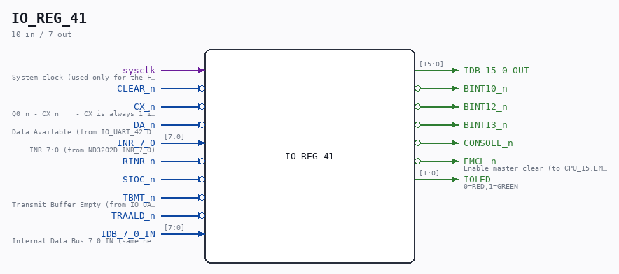
Schematic
Drawn from the Verilog: the yosys netlist of the Simulation (Verilator) build, instance CORE.CPU_BOARD.IO.REG_MODULE. Sub-modules are boxes (click the picture to open it full size; there every sub-module box links to its page, and every wire shows its Verilog name).
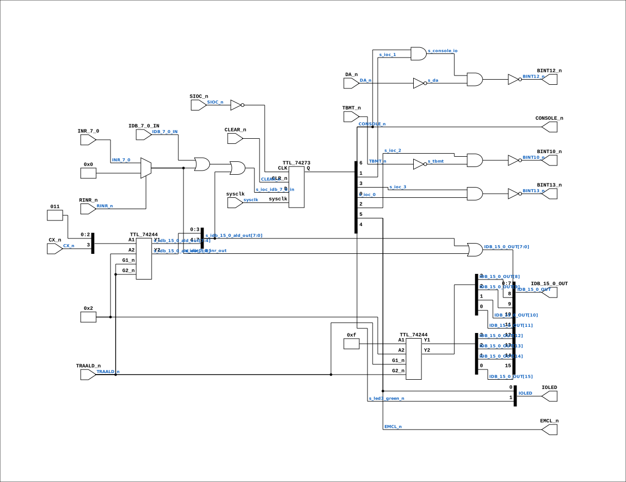
Description
ND120 CPU, MM&M IO/REG IOC, ALD & INR REGS SHEET 41 of 50 Last reviewed: 2-FEB-2025 Ronny Hansen
Ports
| Direction | Width | Name | Description |
|---|---|---|---|
| input | 1 |
sysclk |
System clock (used only for the FF-mode strobe edge-capture) |
| input | 1 |
CLEAR_n (active low) |
|
| input | 1 |
CX_n (active low) |
Q0_n - CX_n - CX is always 1 in the fast version (CX_n = 0) (from PAL_44601B.CX_n) |
| input | 1 |
DA_n (active low) |
Data Available (from IO_UART_42.DA_n) |
| input | [7:0] |
INR_7_0 |
INR 7:0 (from ND3202D.INR_7_0) |
| input | 1 |
RINR_n (active low) |
|
| input | 1 |
SIOC_n (active low) |
|
| input | 1 |
TBMT_n (active low) |
Transmit Buffer Empty (from IO_UART_42.TBMT_n) |
| input | 1 |
TRAALD_n (active low) |
|
| input | [7:0] |
IDB_7_0_IN |
Internal Data Bus 7:0 IN (same net as IO_UART_42.IDB_7_0_IN) |
| output | [15:0] |
IDB_15_0_OUT |
|
| output | 1 |
BINT10_n (active low) |
|
| output | 1 |
BINT12_n (active low) |
|
| output | 1 |
BINT13_n (active low) |
|
| output | 1 |
CONSOLE_n (active low) |
|
| output | 1 |
EMCL_n (active low) |
Enable master clear (to CPU_15.EMCL_n) |
| output | [1:0] |
IOLED |
0=RED,1=GREEN |
Verilog source
Verilog/CPU-BOARD-3202/circuit/IO_REG_41.v on GitHub.
Show the Verilog of IO_REG_41 (352 lines)
/**************************************************************************
** ND120 CPU, MM&M                                                       **
** IO/REG                                                                **
** IOC, ALD & INR REGS                                                   **
** SHEET 41 of 50                                                        **
**                                                                       **
** Last reviewed: 2-FEB-2025                                             **
** Ronny Hansen                                                          **
***************************************************************************/
module IO_REG_41 (
    input       sysclk,  //! System clock (used only for the FF-mode strobe edge-capture)

    // Input signals
    input       CLEAR_n,
    input       CX_n,    //! Q0_n - CX_n    - CX is always 1 in the fast version (CX_n = 0) (from PAL_44601B.CX_n)
    input       DA_n,    //! Data Available (from IO_UART_42.DA_n)
    input [7:0] INR_7_0,  //! INR 7:0 (from ND3202D.INR_7_0)
    input       RINR_n,
    input       SIOC_n,
    input       TBMT_n,  //! Transmit Buffer Empty (from IO_UART_42.TBMT_n)
    input       TRAALD_n,


    // Input and output signals
    input  [ 7:0] IDB_7_0_IN,  //! Internal Data Bus 7:0 IN (same net as IO_UART_42.IDB_7_0_IN)
    output [15:0] IDB_15_0_OUT,

    // Output signals
    output       BINT10_n,
    output       BINT12_n,
    output       BINT13_n,
    output       CONSOLE_n,
    output       EMCL_n,  //! Enable master clear (to CPU_15.EMCL_n)
    output [1:0] IOLED       // 0=RED,1=GREEN
);


  /*******************************************************************************
   ** The wires are defined here                                                 **
   *******************************************************************************/


  wire [ 2:0] s_print_no;
  wire [ 3:0] s_ALD;

  wire [ 7:0] s_inr_7_0;

  wire [ 7:0] s_idb_7_0_in;
  wire [ 7:0] s_ioc_idb_7_0_in;

  wire [15:0] s_idb_15_0_out;
  wire [ 7:0] s_idb_7_0_inr_out;
  wire [15:0] s_idb_15_0_ald_out;


  wire        s_bint10_n;
  wire        s_bint12_n;
  wire        s_bint13_n;
  wire        s_clear_n;
  wire        s_console_io;
  wire        s_cx_n;
  wire        s_da;
  wire        s_ioc_0;
  wire        s_ioc_1;
  wire        s_ioc_2;
  wire        s_ioc_3;
  wire        s_emcl_n;
  wire        s_led3_green_n;
  wire        s_rinr_n;
  wire        s_scons_n;
  wire        s_sioc_n;
  wire        s_strap_5;
  wire        s_strap_6;
  wire        s_strap_7;
  wire        s_strap_8;
  wire        s_strap_9;
  wire        s_tbmt;
  wire        s_traald_n;

  /* verilator lint_off UNUSEDSIGNAL */
  (* keep = "true", DONT_TOUCH = "true" *) wire s_reset;
  /* verilator lint_on UNUSEDSIGNAL */


  /*******************************************************************************
   ** The module functionality is described here                                 **
   *******************************************************************************/

  /*******************************************************************************
   ** Here all input connections are defined                                     **
   *******************************************************************************/
  assign s_inr_7_0[7:0] = INR_7_0;
  assign s_rinr_n = RINR_n;
  assign s_sioc_n = SIOC_n;
  assign s_cx_n = CX_n;
  assign s_tbmt = !TBMT_n;
  assign s_clear_n = CLEAR_n;
  assign s_da = !DA_n;
  assign s_traald_n = TRAALD_n;
  assign s_idb_7_0_in = IDB_7_0_IN;

  /*******************************************************************************
   ** Here all output connections are defined                                    **
   *******************************************************************************/
  assign BINT10_n = s_bint10_n;
  assign BINT12_n = s_bint12_n;
  assign BINT13_n = s_bint13_n;
  assign CONSOLE_n = s_scons_n;
  assign EMCL_n = s_emcl_n;
  assign IDB_15_0_OUT = s_idb_15_0_out[15:0];


  /*******************************************************************************
   ** Here all in-lined components are defined                                   **
   *******************************************************************************/

  assign s_ioc_idb_7_0_in[7:0] = s_idb_7_0_in[7:0] | s_idb_7_0_inr_out[7:0] | s_idb_15_0_ald_out[7:0];


  // PRINT VERSION = 011 FOR VERSION D
  assign s_print_no[2:0] = 3'b011;  // 011 == 3202D


  // Constant for ALD register ECO Fixes // Set to ECO 100-785. Strap on 6,8 and 9
  // Setting a physical strap enables pull low/0 else its pulled high.
  assign s_strap_9 = 1'b0;  // STRAP9 => IDB8
  assign s_strap_8 = 1'b0;  // STRAP8 => IDB9
  assign s_strap_7 = 1'b1;  // STRAP7 => IDB10
  assign s_strap_6 = 1'b0;  // STRAP6 => IDB11
  assign s_strap_5 = 1'b1;  // STRAP5 => IDB12


  // Constant for ALD settings. ALD boot switch (for options, see comment at end of this file)
  // 07-AUG-2026 (Ronny): default boot is the WINCHESTER. Vector 0010 (2) =
  // switch setting 13 in the table below = "Bootstrap load from Winchester
  // disk (500) and run" - block 0 into memory, execution from address 20
  // (note 3). A bare '&' (or the LOAD button) now boots the disc; the paper
  // tape stays reachable explicitly with 400$ / 400&.
  // Previous value: 4'b0100 (switch 11, BPUN load from 400 paper tape).
  assign s_ALD[3:0] = 4'b0010;  //  0010 (2) == bootstrap load Winchester 500, run from 20.


  // CPU BOARD LED: RED (lights while MASTER CLEAR is running) ACTIVE LOW.
  // Active low is MEASURED: the MiSTer port passed these through un-inverted
  // on 31-AUG-2026 and every lamp came out backwards, so its console inverts
  // both (fpga/mister/nd120.sv:511-518) and GREEN lights correctly there.
  // The IOC register comments below say "red LED ON1" / "green LED on1";
  // reading those as active-high and dropping the inversion is exactly the
  // mistake made on 01-SEP-2026. The measurement wins.
  assign IOLED[0] = s_emcl_n;

  // CPU BOARD LED: GREEN (initialisation completed, i.e. the microcode
  // reached MACL2 and the self-test passed) ACTIVE LOW - see above.
  assign IOLED[1] = s_led3_green_n;

  /*******************************************************************************
   ** Here all normal components are defined                                     **
   *******************************************************************************/
  assign s_console_io = s_scons_n & s_ioc_1;
  assign s_bint13_n = ~(s_ioc_3 & s_ioc_0);
  assign s_bint10_n = ~(s_ioc_2 & s_tbmt);
  assign s_bint12_n = ~(s_console_io & s_da);


  /*******************************************************************************
   ** Here all sub-circuits are defined                                          **
   *******************************************************************************/


   // NOTE: CHIP_28A_IOC CLK() signal has been negated to get code to work. This is different than the original drawings

  // P3 (docs/plan-fix-unconstrained-clocks.md): SIOC_n is an IDB write
  // strobe, not a clock. In FF mode the IOC register captures on a
  // sysclk-detected strobe rise instead of clocking on the routed net.
`ifdef FPGA_FF_MODE
  localparam SIOC_CAPTURE = 2;
`else
  localparam SIOC_CAPTURE = 0;
`endif

  TTL_74273 #(.USE_SYSCLK(SIOC_CAPTURE)) CHIP_28A_IOC (
      .sysclk(sysclk),
      .CLK(~s_sioc_n),  // Clock input (in drawings using s_sioc_n, but had to invert to get the correct behaviour)
      .CLR_n(s_clear_n),  // Active low clear input
      .D(s_ioc_idb_7_0_in[7:0]), // 8-bit data input directly from the bus (which is a combination of IDB, ALD and INR)
      .Q({
        s_reset,           // 8-bit output, bit 7 (Q1) - (Reset real time clock.)
        s_scons_n,         // 8-bit output, bit 6 (Q2) - (Set terminal #1 in OPCOM (console), as opposed to normal)
        s_emcl_n,          // 8-bit output, bit 5 (Q3) -> EMCL_n (Enable master clear: red LED ON1)
        s_led3_green_n,    // 8-bit output, bit 4 (Q4) - (Initialisation completed: green LED on1)

        s_ioc_3,  // 8-bit output, bit 3 (Q5) - (clock interrupt generated from RTC trap handler.)
        s_ioc_2,  // 8-bit output, bit 2 (Q6) - (enable output interrupt on level 10, from terminal #1 ->UART transmit buffer empty)
        s_ioc_1,  // 8-bit output, bit 1 (Q7) - (enable input interrupt on level 12, from terminal #1 -> UART data available)
        s_ioc_0   // 8-bit output, bit 0 (Q8) - (enable clock interrupt on level 13.)
      })
  );


`ifdef ND120_IOR_PROBE
  // DIAGNOSTIC (IDENT PL10 hunt, 20-AUG-2026): log IOC control-register loads
  // and BINT10_n edges so the interrupt-enable state at each level-10
  // dispatch is on record. Sim-only, no logic effect.
  reg [7:0] r_iorp_ioc_prev;
  reg       r_iorp_b10_prev;
  always @(posedge sysclk) begin
    if (r_iorp_ioc_prev != {s_reset, s_scons_n, s_emcl_n, s_led3_green_n,
                            s_ioc_3, s_ioc_2, s_ioc_1, s_ioc_0})
      $display("[ior] t=%0t IOC=%b (rst,cons_n,emcl_n,led_n,i3,i2,i1,i0)",
               $time, {s_reset, s_scons_n, s_emcl_n, s_led3_green_n,
                       s_ioc_3, s_ioc_2, s_ioc_1, s_ioc_0});
    if (s_bint10_n != r_iorp_b10_prev)
      $display("[ior] t=%0t BINT10_n=%b (ioc2=%b tbmt=%b)",
               $time, s_bint10_n, s_ioc_2, s_tbmt);
    r_iorp_ioc_prev <= {s_reset, s_scons_n, s_emcl_n, s_led3_green_n,
                        s_ioc_3, s_ioc_2, s_ioc_1, s_ioc_0};
    r_iorp_b10_prev <= s_bint10_n;
  end
`endif

  // TTL_74244 CHIP_24A_INR (simplified..)
  assign s_idb_7_0_inr_out[7:0] = s_rinr_n ? 8'b0 : s_inr_7_0[7:0];

  // IDB bus 7:0 is shared between ALD and INR.. or Z state
  assign s_idb_15_0_out[7:0] = s_idb_15_0_ald_out[7:0] | s_idb_7_0_inr_out[7:0];
  assign s_idb_15_0_out[15:8] = s_idb_15_0_ald_out[15:8];


  // ALD register, STRAP bits  + CX and print version
  TTL_74244 CHIP_27A_STRAP (
      // Input
      //        1A4                1A3                  1A2                  1A1
      .A1  ({s_strap_5, 1'b1, 1'b1, 1'b1}),
      .G1_n(s_traald_n),

      //        2A4                2A3                  2A2                  2A1
      .A2  ({s_strap_9, s_strap_8, s_strap_7, s_strap_6}),
      .G2_n(s_traald_n),


      // Output
      .Y1({
        s_idb_15_0_ald_out[12],
        s_idb_15_0_ald_out[13],
        s_idb_15_0_ald_out[14],
        s_idb_15_0_ald_out[15]
      }),
      .Y2({
        s_idb_15_0_ald_out[8], s_idb_15_0_ald_out[9], s_idb_15_0_ald_out[10], s_idb_15_0_ald_out[11]
      })
  );


  TTL_74244 CHIP_25A_ALD (
      // Input
      //        1A1                1A2                  1A3                  1A4
      .A1  ({s_cx_n, s_print_no[2], s_print_no[1], s_print_no[0]}),
      .G1_n(s_traald_n),

      //        2A1                2A2                  2A3                  2A4
      .A2  ({s_ALD[3], s_ALD[2], s_ALD[1], s_ALD[0]}),
      .G2_n(s_traald_n),


      // Output
      .Y1({
        s_idb_15_0_ald_out[7], s_idb_15_0_ald_out[6], s_idb_15_0_ald_out[5], s_idb_15_0_ald_out[4]
      }),
      .Y2({
        s_idb_15_0_ald_out[3], s_idb_15_0_ald_out[2], s_idb_15_0_ald_out[1], s_idb_15_0_ald_out[0]
      })
  );

`ifdef ND120_INT12_PROBE
  // Sim-only diagnostic (24-AUG TPE deaf-prompt hunt): log the console
  // interrupt enables (IOC bits), DA, and the BINT10/12/13 lines on every
  // change. Shows whether TPE ever enables the console input interrupt
  // (IOC1) and whether BINT12 fires when a character arrives.
  reg [7:0] r_i12_prev;
  always @(posedge sysclk) begin : int12_probe
    reg [7:0] now;
    now = {s_ioc_0, s_ioc_1, s_ioc_2, s_ioc_3, s_da, s_bint10_n, s_bint12_n, s_bint13_n};
    if (now != r_i12_prev)
      $display("[int12] t=%0t ioc0=%b ioc1=%b ioc2=%b ioc3=%b da=%b bint10_n=%b bint12_n=%b bint13_n=%b",
               $time, now[7], now[6], now[5], now[4], now[3], now[2], now[1], now[0]);
    r_i12_prev <= now;
  end
  // log every SIOC strobe with the IDB byte being written to the IOC
  // register - distinguishes "TPE never asks for the input interrupt"
  // from "the FF-mode strobe capture lost bit 1".
  reg r_i12_sioc_prev;
  always @(posedge sysclk) begin
    if (!s_sioc_n && r_i12_sioc_prev)
      $display("[int12] t=%0t SIOC write IDB=%03o", $time, s_ioc_idb_7_0_in);
    r_i12_sioc_prev <= s_sioc_n;
  end
`endif

endmodule


/*

(Mapped from ND-110 and ND-120 microcode (they are identical)

+--------+------------------+-------------------+-----------------------------------------------------------------------
|SWITCH  | ALD VECTOR (hex) | ALD VALUE (octal) | DESCRIPTION
+--------+------------------+-------------------+-----------------------------------------------------------------------
|15      |     x0           | 0                 | (Note 2)
|14      |     x1           | 1560              | Switch setting 14 -  BPUN load from floppy (1560) and run (*3)
|13      |     x2           | 20500             | Bootstrap load from Winchester disk (500) and run (*3)
|12      |     x3           | 21540             | Bootstrap load from SMD disk (1540,) and run (*3)
|11      |     x4           | 400               | BPUN load from paper tape (400) and run (*3)
|10      |     x5           | 1600              | BPUN load from HDLC (1600) and run (*3)
|9       |     x6           | 21560             | Run (*3) (No load)
|8       |     x7           | 0                 | Run (*3) (No load)
|7       |     x8           | 100000            | (Note 2)
|6       |     x9           | 101560            | Binary load from 1560 (SCSI boot use this setting..?)
|5       |     xA           | 120500            | Mass storage from 500
|4       |     xB           | 121540            | Mass storage from 1540 (SMD disk)
|3       |     xC           | 100400            | Binary load from 400 (paper tape reader)
|2       |     xD           | 101600            | Switch setting 2 -  Binary load from 1600 (HDLC)
|1       |     xE           | 121560            |
|0       |     xF           | 100000            |
+--------+------------------+-------------------+-----------------------------------------------------------------------

Note 1: The action will be taken if
      a. $ or & (without preceding value) has been typed on the console in OPCOM mode
      b. The [LOAD] button has been pressed
      c. The power has been restored and the keyswitch in the lock positon, but the standby power has been lost (extended power failure).

Note 2: No load. The CPU is put in STOP made.

Note 3: Run from address 20.

Note 4:
The content of the internal register I12 reflects the ALD settings.

ALD switch settings 8 to 15 specify load and run, settings 2 to 7 specify load only.
ALD settings 4, 5, 12 and 13 specify a bootstrap load from a disk.
All other settings expect BPUN format.

The start address is always the power fail restart address (20).


* Load from an operator specified address
To specify a bootstrap load set bit 13 of the device address to 1 (i.e. if the device address is 1550 enter 21550&)


*/