CPU_CS_CTL_18
Source: Verilog/CPU-BOARD-3202/circuit/CPU_CS_CTL_18.v
Where it sits (Simulation): ND120_TOP > ND120_CORE > ND3202D > CPU_15 > CPU_CS_16 > CPU_CS_CTL_18
- instance path: CORE.CPU_BOARD.CPU.CS.CTL
Used in: CPU_CS_16 (all tops)
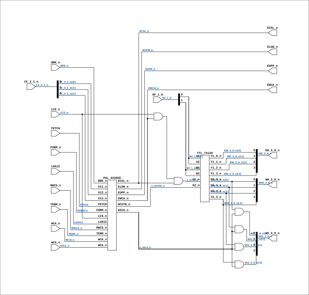
Contains: PAL_44305D, TTL_74139
Module hierarchy - All modules
Schematic
Drawn from the Verilog: the yosys netlist of the Simulation (Verilator) build, instance CORE.CPU_BOARD.CPU.CS.CTL. Sub-modules are boxes (click the picture to open it full size; there every sub-module box links to its page, and every wire shows its Verilog name).
Description
ND120 CPU, MM&M CPU/CS/CTL CS CONTROL SHEET 18 of 50 Last reviewed: 21-APRIL-2024 Ronny Hansen
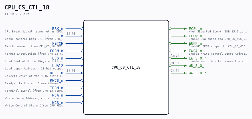
Ports
| Direction | Width | Name | Description |
|---|---|---|---|
| input | 1 |
BRK_n (active low) |
CPU Break Signal (same net as CPU_15.BRK_n) |
| input | [2:0] |
CC_3_1_n (active low) |
Cache control bits 3:1 (from CPU_15.CC_3_1_n) |
| input | 1 |
FETCH |
Fetch command (from CPU_CS_16.FETCH) |
| input | 1 |
FORM_n (active low) |
Format instruction (from CPU_15.FORM_n) |
| input | 1 |
LCS_n (active low) |
Load Control Store (Negated) (from CPU_CS_16.LCS_n) |
| input | 1 |
LUA12 |
Load Upper Address - 13-bit output for upper address bits of control store (same net as CPU_CS_16.LUA_12_0[12]) |
| input | [1:0] |
RF_1_0 |
Selects which of the 4 16 bit's of the microcode to fetch from ROM (from CPU_PROC_32.RF_1_0) |
| input | 1 |
RWCS_n (active low) |
Read/Write Control Store (low=write) (from CPU_CS_16.RWCS_n) |
| input | 1 |
TERM_n (active low) |
Terminal signal (from CPU_15.TERM_n) |
| input | 1 |
WCA_n (active low) |
Write Cache Address, controls writing to the cache address register (from CPU_MMU_24.WCA_n) |
| input | 1 |
WCS_n (active low) |
Write Control Store (from CPU_PROC_32.WCS_n) |
| output | 1 |
ECSL_n (active low) |
When asserted (low), IDB 15:0 is connected to IDB 15:0. (to CPU_CS_TCV_20.ECSL_n) |
| output | 1 |
ELOW_n (active low) |
Enable LOW chips (to CPU_CS_WCS_21_22.ELOW_n) |
| output | 1 |
EUPP_n (active low) |
Enable UPPER chips (to CPU_CS_WCS_21_22.EUPP_n) |
| output | 1 |
EWCA_n (active low) |
Enable Write Control Store Address - Active low signal to enable writing to control store address (to CPU_CS_16.EWCA_n) |
| output | [3:0] |
EW_3_0_n (active low) |
Enable Word (4 bits, where the enabled word (0-3) has its bit set to 0. (to CPU_CS_TCV_20.EW_3_0_n) |
| output | [3:0] |
WU_3_0_n (active low) |
|
| output | [3:0] |
WW_3_0_n (active low) |
Verilog source
Verilog/CPU-BOARD-3202/circuit/CPU_CS_CTL_18.v on GitHub.
Show the Verilog of CPU_CS_CTL_18 (165 lines)
/**************************************************************************
** ND120 CPU, MM&M                                                       **
** CPU/CS/CTL                                                            **
** CS CONTROL                                                            **
** SHEET 18 of 50                                                        **
**                                                                       **
** Last reviewed: 21-APRIL-2024                                          **
** Ronny Hansen                                                          **
***************************************************************************/

module CPU_CS_CTL_18 (
    // Input signals
    input       BRK_n,  //! CPU Break Signal (same net as CPU_15.BRK_n)
    input [2:0] CC_3_1_n,  //! Cache control bits 3:1 (from CPU_15.CC_3_1_n)
    input       FETCH,  //! Fetch command (from CPU_CS_16.FETCH)
    input       FORM_n,  //! Format instruction (from CPU_15.FORM_n)
    input       LCS_n,  //! Load Control Store (Negated) (from CPU_CS_16.LCS_n)
    input       LUA12,  //! Load Upper Address - 13-bit output for upper address bits of control store (same net as CPU_CS_16.LUA_12_0[12])
    input [1:0] RF_1_0,  //! Selects which of the 4 16 bit's of the microcode to fetch from ROM (from CPU_PROC_32.RF_1_0)
    input       RWCS_n,  //! Read/Write Control Store (low=write) (from CPU_CS_16.RWCS_n)
    input       TERM_n,  //! Terminal signal (from CPU_15.TERM_n)
    input       WCA_n,  //! Write Cache Address, controls writing to the cache address register (from CPU_MMU_24.WCA_n)
    input       WCS_n,  //! Write Control Store (from CPU_PROC_32.WCS_n)

    // Output signals
    output       ECSL_n,  //! When asserted (low), IDB 15:0 is connected to IDB 15:0. (to CPU_CS_TCV_20.ECSL_n)
    output       ELOW_n,  //! Enable LOW chips (to CPU_CS_WCS_21_22.ELOW_n)
    output       EUPP_n,  //! Enable UPPER chips (to CPU_CS_WCS_21_22.EUPP_n)
    output       EWCA_n,  //! Enable Write Control Store Address - Active low signal to enable writing to control store address (to CPU_CS_16.EWCA_n)
    output [3:0] EW_3_0_n,  //! Enable Word (4 bits, where the enabled word (0-3) has its bit set to 0. (to CPU_CS_TCV_20.EW_3_0_n)
    output [3:0] WU_3_0_n,
    output [3:0] WW_3_0_n
);


  /*******************************************************************************
   ** The wires are defined here                                                 **
   *******************************************************************************/
  wire [3:0] s_ew_3_0_n;
  wire [3:0] s_wu_3_0_n;
  wire [1:0] s_rf_1_0;
  wire [3:0] s_ww_3_0_n;
  wire [2:0] s_cc_3_1_n;
  wire       s_brk_n;
  wire       s_ecsd_n;
  wire       s_ecsl_n;
  wire       s_elow_n;
  wire       s_eupp_n;
  wire       s_ewca_n;
  wire       s_fetch;
  wire       s_form_n;
  wire       s_lcs_n;
  wire       s_lua12;
  wire       s_rwcs_n;
  wire       s_term_n;
  wire       s_WCA_n;
  wire       s_wcs_n;
  wire       s_wcstb_n;
  wire       s_wica_n;

  /*******************************************************************************
   ** Here all input connections are defined                                     **
   *******************************************************************************/
  assign s_rf_1_0[1:0]   = RF_1_0;
  assign s_cc_3_1_n[2:0] = CC_3_1_n;
  assign s_fetch         = FETCH;
  assign s_wcs_n         = WCS_n;
  assign s_brk_n         = BRK_n;
  assign s_lcs_n         = LCS_n;
  assign s_lua12         = LUA12;
  assign s_term_n        = TERM_n;
  assign s_WCA_n         = WCA_n;
  assign s_form_n        = FORM_n;
  assign s_rwcs_n        = RWCS_n;

  /*******************************************************************************
   ** Here all output connections are defined                                    **
   *******************************************************************************/
  assign ECSL_n          = s_ecsl_n;
  assign ELOW_n          = s_elow_n;
  assign EUPP_n          = s_eupp_n;
  assign EWCA_n          = s_ewca_n;
  assign EW_3_0_n        = s_ew_3_0_n[3:0];
  assign WU_3_0_n        = s_wu_3_0_n[3:0];
  assign WW_3_0_n        = s_ww_3_0_n[3:0];

  /*******************************************************************************
   ** Here all normal components are defined                                     **
   *******************************************************************************/
  // ECSD enables the 74139 that produces EW_3_0_n - the word select telling the
  // CS transceiver WHICH 16-bit slice of the 64-bit control-store word faces the
  // IDB. It must be active for the whole data window in BOTH directions.
  //
  // 07-AUG-2026: ECSL was missing from this enable, and that is why TRA CS
  // (150017) returned 0 - SINTRAN's microcode-revision test
  // (PH-P2-RESTART.NPL: X:=100 ; *150017 ; IF A<<13 -> "Micro-code not loaded.
  // CPU revision too low !!"). Measured in the waveform: during the ACS
  // routine's RWCS word the addressed CS word DID reach the IDB (142001, the
  // low slice of WCS word 0), but only for a single sample - EWCA drops as the
  // cycle enters CC3, EW went to 17 (no slice selected) and the data vanished
  // before the CGA captured it, while ECSL was still holding the read window
  // open ("ECSL HOLD IN g AND h", PAL_44305D). Adding ECSL_n here keeps the
  // slice selected for exactly the window the read is defined over.
  //
  // This can not create a spurious drive: CPU_CS_TCV_20 only puts data on the
  // IDB when ECSL_n is low AND WCS_n is high (read), and only writes CSBITS
  // when WCS_n is low - and ECSL itself requires WCS_n high, so the write
  // direction is untouched. Fails identically in latch and FF mode, so this is
  // an original transcription gap, not a clock-enable artifact.
  assign s_ecsd_n        = s_lcs_n & s_ewca_n & s_ecsl_n;

  // Simplified logic for WU_3_0_n, a NOR chip with negated inputs is in reality an AND chip
  assign s_wu_3_0_n[0]   = s_ww_3_0_n[0] & s_wica_n;
  assign s_wu_3_0_n[1]   = s_ww_3_0_n[1] & s_wica_n;
  assign s_wu_3_0_n[2]   = s_ww_3_0_n[2] & s_wica_n;
  assign s_wu_3_0_n[3]   = s_ww_3_0_n[3] & s_wica_n;


  /*******************************************************************************
   ** Here all sub-circuits are defined                                          **
   *******************************************************************************/

  // Note! EW_3_0_n will only be enbled when ECSL_n is gone high - and the PAL 44305D signal EWCA_n is also high.

  TTL_74139 CHIP_30B (
      .A1(s_rf_1_0[0]),
      .B1(s_rf_1_0[1]),
      .G1_n(s_ecsd_n),
      .Y1_0_n(s_ew_3_0_n[0]),
      .Y1_1_n(s_ew_3_0_n[1]),
      .Y1_2_n(s_ew_3_0_n[2]),
      .Y1_3_n(s_ew_3_0_n[3]),

      .A2(s_rf_1_0[0]),
      .B2(s_rf_1_0[1]),
      .G2_n(s_wcstb_n),
      .Y2_0_n(s_ww_3_0_n[0]),
      .Y2_1_n(s_ww_3_0_n[1]),
      .Y2_2_n(s_ww_3_0_n[2]),
      .Y2_3_n(s_ww_3_0_n[3])
  );

  PAL_44305D PAL_44305_UCSCTL (
      .FORM_n (s_form_n),       //! input FORM_n - I0
      .CC1_n  (s_cc_3_1_n[0]),  //! input CC1_n  - I1 - Cycle Control 1 (b+c+d+e+j+k+l+m)
      .CC2_n  (s_cc_3_1_n[1]),  //! input CC2_n  - I2 - Cycle control 2 (e+f+g+h+i+j+k)
      .CC3_n  (s_cc_3_1_n[2]),  //! input CC3_n  - I3 - Cycle Control 3 (h+i+j+k+l+m+n+o)
      .LCS_n  (s_lcs_n),        //! input LCS_n  - I4 - Load Control Store (negated)
      .RWCS_n (s_rwcs_n),       //! input RWCS_n - I5 - Read/Write Control Store (low=write)
      .WCS_n  (s_wcs_n),        //! input WCS_n  - I6 - Write Control Store (negated)
      .FETCH  (s_fetch),        //! input FETCH  - I7 - Fetch
      .BRK_n  (s_brk_n),        //! input BRK_n  - I8 -
      .TERM_n (s_term_n),       //! input TERM_n - I9 -
      .WICA_n (s_wica_n),       //! output Y0_n - WICA_n
      .WCSTB_n(s_wcstb_n),      //! output Y1_n - WCSTB_n
      .ECSL_n (s_ecsl_n),       //! output B0_n - ECSL_n
      .EWCA_n (s_ewca_n),       //! output B1_n - EWCA_n
      .EUPP_n (s_eupp_n),       //! output B2_n - EUPP_n
      .ELOW_n (s_elow_n),       //! output B3_n - ELOW_n
      .WCA_n  (s_WCA_n),        //! input B4_n WCA_n
      .LUA12  (s_lua12)         //! input B5_n LUA12
  );

endmodule