CPU_MMU_PTIDB_30
Source: Verilog/CPU-BOARD-3202/circuit/CPU_MMU_PTIDB_30.v
Where it sits (Simulation): ND120_TOP > ND120_CORE > ND3202D > CPU_15 > CPU_MMU_24 > CPU_MMU_PTIDB_30
- instance path: CORE.CPU_BOARD.CPU.MMU.PTIDB
Used in: CPU_MMU_24 (all tops)
Contains: no other modules.
Module hierarchy - All modules
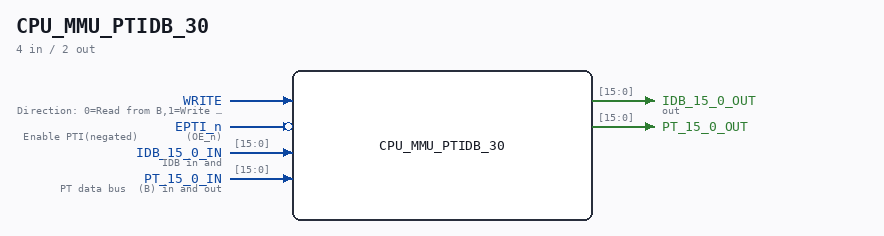
Schematic
Drawn from the Verilog: the yosys netlist of the Simulation (Verilator) build, instance CORE.CPU_BOARD.CPU.MMU.PTIDB. Sub-modules are boxes (click the picture to open it full size; there every sub-module box links to its page, and every wire shows its Verilog name).
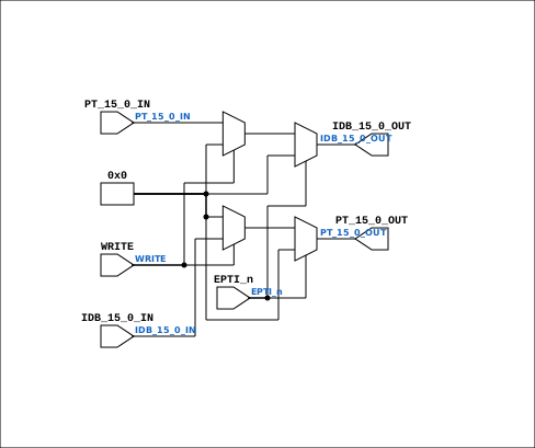
Description
ND120 CPU, MM&M CPU/MMU/PTIDB PT TO IDB SHEET 30 of 50 Last reviewed: 2-FEB-2025 Ronny Hansen
Ports
| Direction | Width | Name | Description |
|---|---|---|---|
| input | 1 |
WRITE |
Direction: 0=Read from B,1=Write to B (DIR) |
| input | 1 |
EPTI_n (active low) |
Enable PTI(negated) (OE_n) |
| input | [15:0] |
IDB_15_0_IN |
IDB in and |
| output | [15:0] |
IDB_15_0_OUT |
out |
| input | [15:0] |
PT_15_0_IN |
PT data bus (B) in and out |
| output | [15:0] |
PT_15_0_OUT |
Verilog source
Verilog/CPU-BOARD-3202/circuit/CPU_MMU_PTIDB_30.v on GitHub.
Show the Verilog of CPU_MMU_PTIDB_30 (51 lines)
/**************************************************************************
** ND120 CPU, MM&M                                                       **
** CPU/MMU/PTIDB                                                         **
** PT TO IDB                                                             **
** SHEET 30 of 50                                                        **
**                                                                       **
** Last reviewed: 2-FEB-2025                                             **
** Ronny Hansen                                                          **
***************************************************************************/

// verilator lint_off ASSIGNDLY

module CPU_MMU_PTIDB_30 (
  input WRITE,  // Direction: 0=Read from B,1=Write to B  (DIR)
  input EPTI_n, // Enable PTI(negated)        (OE_n)

  input  [15:0] IDB_15_0_IN,  // IDB in and
  output [15:0] IDB_15_0_OUT, //             out

  input  [15:0] PT_15_0_IN,  //PT data bus  (B) in and out
  output [15:0] PT_15_0_OUT  //
);

  // This code replaces the original Logisim generated code with a simpler and more efficient implementation
  // It replaces two 74PCT245 chips (8-bit transceiver with 3-state outputs) with one 16 bit identical implementation.

  wire OE_n;
  wire DIR;

  assign OE_n  = EPTI_n;
  assign DIR   = WRITE;


  reg [15:0] A_reg;
  reg [15:0] B_reg;

  always @(*)
  begin
    A_reg = IDB_15_0_IN;
    B_reg = PT_15_0_IN;
  end

  // Drive logic for IDB_15_0 and PT_15_0

  // Set IDB to B value IF DIR=0 (read) else to 3-state
  assign IDB_15_0_OUT = OE_n ? 16'b0 : !DIR ? B_reg : 16'b0;

  // Set PT to A value IF DIR=1 (write) else to 3-state
  assign PT_15_0_OUT  = OE_n ? 16'b0 : DIR ? A_reg : 16'b0;

endmodule