IO_37
Source: Verilog/CPU-BOARD-3202/circuit/IO_37.v
Where it sits (Simulation): ND120_TOP > ND120_CORE > ND3202D > IO_37
- instance path: CORE.CPU_BOARD.IO
Used in: ND3202D (all tops)
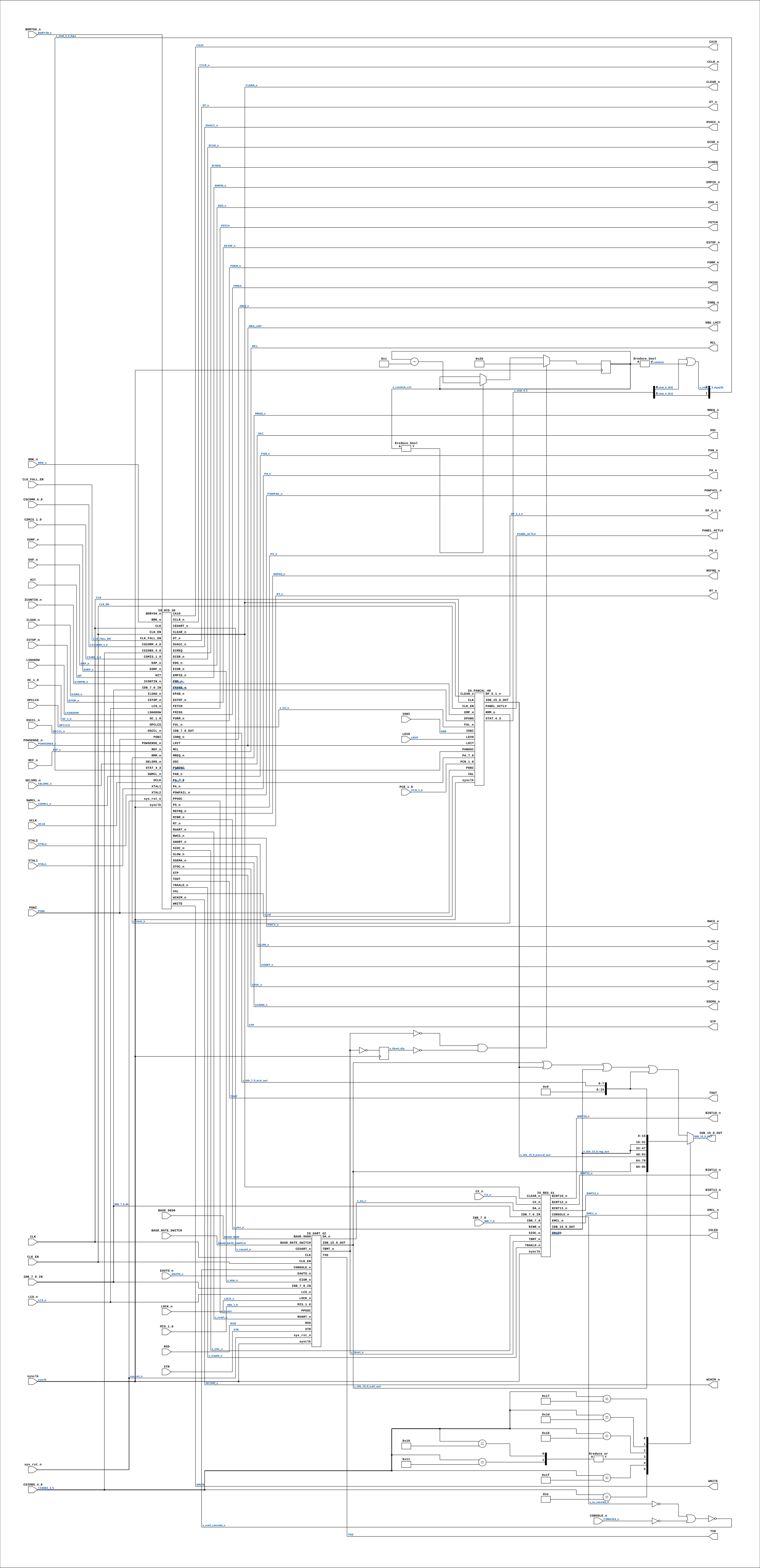
Contains: IO_DCD_38, IO_PANCAL_40, IO_REG_41, IO_UART_42
Module hierarchy - All modules
Schematic
Drawn from the Verilog: the yosys netlist of the Simulation (Verilator) build, instance CORE.CPU_BOARD.IO. Sub-modules are boxes (click the picture to open it full size; there every sub-module box links to its page, and every wire shows its Verilog name).
Description
ND120 CPU, MM&M IO IO TOP LEVEL SHEET 37 of 50 Last reviewed: 22-MAR-2025 Ronny Hansen
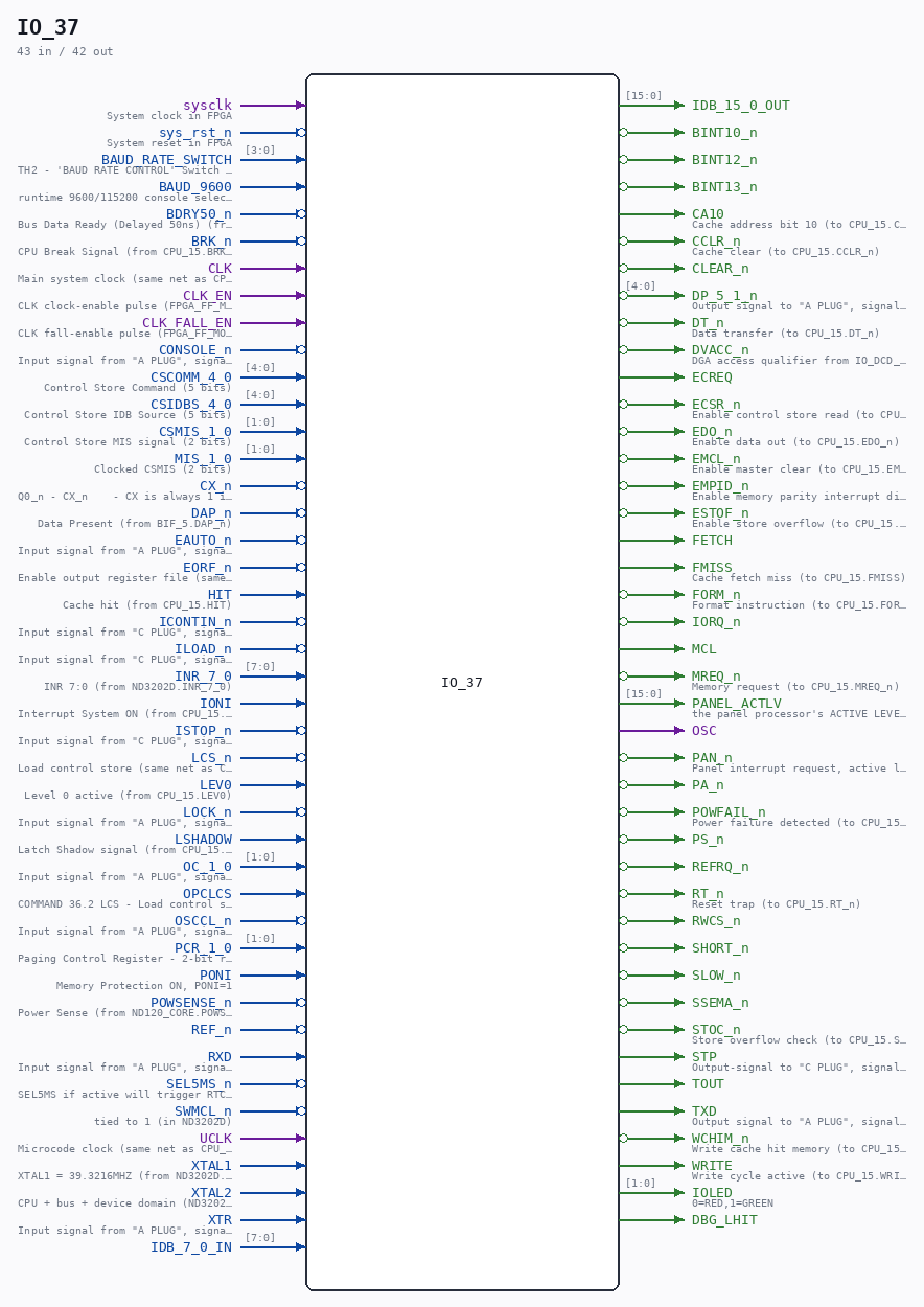
Ports
| Direction | Width | Name | Description |
|---|---|---|---|
| input | 1 |
sysclk |
System clock in FPGA |
| input | 1 |
sys_rst_n (active low) |
System reset in FPGA |
| input | [3:0] |
BAUD_RATE_SWITCH |
TH2 - 'BAUD RATE CONTROL' Switch on the PCB to select baudrate (from ND3202D.BAUD_RATE_SWITCH) |
| input | 1 |
BAUD_9600 |
runtime 9600/115200 console select -> IO_UART_42 -> SC2661 |
| input | 1 |
BDRY50_n (active low) |
Bus Data Ready (Delayed 50ns) (from BIF_5.BDRY50_n) |
| input | 1 |
BRK_n (active low) |
CPU Break Signal (from CPU_15.BRK_n) |
| input | 1 |
CLK |
Main system clock (same net as CPU_15.CLK) |
| input | 1 |
CLK_EN |
CLK clock-enable pulse (FPGA_FF_MODE, else 0) |
| input | 1 |
CLK_FALL_EN |
CLK fall-enable pulse (FPGA_FF_MODE, else 0) |
| input | 1 |
CONSOLE_n (active low) |
Input signal from "A PLUG", signal C21/C30 - CONSOLE_n (from ND3202D.CONSOLE_n) |
| input | [4:0] |
CSCOMM_4_0 |
Control Store Command (5 bits) |
| input | [4:0] |
CSIDBS_4_0 |
Control Store IDB Source (5 bits) |
| input | [1:0] |
CSMIS_1_0 |
Control Store MIS signal (2 bits) |
| input | [1:0] |
MIS_1_0 |
Clocked CSMIS (2 bits) |
| input | 1 |
CX_n (active low) |
Q0_n - CX_n - CX is always 1 in the fast version (CX_n = 0) (from PAL_44601B.CX_n) |
| input | 1 |
DAP_n (active low) |
Data Present (from BIF_5.DAP_n) |
| input | 1 |
EAUTO_n (active low) |
Input signal from "A PLUG", signal C19 - EAUTO_n (from ND3202D.EAUTO_n) |
| input | 1 |
EORF_n (active low) |
Enable output register file (same net as CPU_15.EORF_n) |
| input | 1 |
HIT |
Cache hit (from CPU_15.HIT) |
| input | 1 |
ICONTIN_n (active low) |
Input signal from "C PLUG", signal B15 - CONTINUE_n (from ND3202D.CONTINUE_n) |
| input | 1 |
ILOAD_n (active low) |
Input signal from "C PLUG", signal B12 - LOAD_n (from ND3202D.LOAD_n) |
| input | [7:0] |
INR_7_0 |
INR 7:0 (from ND3202D.INR_7_0) |
| input | 1 |
IONI |
Interrupt System ON (from CPU_15.IONI) |
| input | 1 |
ISTOP_n (active low) |
Input signal from "C PLUG", signal B16 - STOP_n (from ND3202D.STOP_n) |
| input | 1 |
LCS_n (active low) |
Load control store (same net as CPU_15.LCS_n) |
| input | 1 |
LEV0 |
Level 0 active (from CPU_15.LEV0) |
| input | 1 |
LOCK_n (active low) |
Input signal from "A PLUG", signal B12 - LOCK_n (from ND3202D.LOCK_n) |
| input | 1 |
LSHADOW |
Latch Shadow signal (from CPU_15.LSHADOW) |
| input | [1:0] |
OC_1_0 |
Input signal from "A PLUG", signal C6 (OC0) and A6 (OC1) => (TO IO OC_1_0) (from ND3202D.OC_1_0) |
| input | 1 |
OPCLCS |
COMMAND 36.2 LCS - Load control store from PROM and perform a Master Clear (from CPU_15.OPCLCS) |
| input | 1 |
OSCCL_n (active low) |
Input signal from "A PLUG", signal B3 - OSCCL_n => (TO IO OSCCL_n) (from ND3202D.OSCCL_n) |
| input | [1:0] |
PCR_1_0 |
Paging Control Register - 2-bit register for paging control (from CPU_15.PCR_1_0) |
| input | 1 |
PONI |
Memory Protection ON, PONI=1 |
| input | 1 |
POWSENSE_n (active low) |
Power Sense (from ND120_CORE.POWSENSE_n) |
| input | 1 |
REF_n (active low) |
|
| input | 1 |
RXD |
Input signal from "A PLUG", signal C8 - RXD (to the UART RXD) (from ND3202D.RXD) |
| input | 1 |
SEL5MS_n (active low) |
SEL5MS if active will trigger RTC after 5 ms, not 20ms) (from ND3202D.SEL5MS_n) |
| input | 1 |
SWMCL_n (active low) |
tied to 1 (in ND3202D) |
| input | 1 |
UCLK |
Microcode clock (same net as CPU_15.UCLK) |
| input | 1 |
XTAL1 |
XTAL1 = 39.3216MHZ (from ND3202D.CLOCK_1) |
| input | 1 |
XTAL2 |
CPU + bus + device domain (ND3202D sysclk/CLOCK_1/CLOCK_2) (from ND120_CORE.clk_cpu) |
| input | 1 |
XTR |
Input signal from "A PLUG", signal B4/C23 - XTR => (TO IO XTR) (from ND3202D.XTR) |
| input | [7:0] |
IDB_7_0_IN |
|
| output | [15:0] |
IDB_15_0_OUT |
|
| output | 1 |
BINT10_n (active low) |
|
| output | 1 |
BINT12_n (active low) |
|
| output | 1 |
BINT13_n (active low) |
|
| output | 1 |
CA10 |
Cache address bit 10 (to CPU_15.CA10) |
| output | 1 |
CCLR_n (active low) |
Cache clear (to CPU_15.CCLR_n) |
| output | 1 |
CLEAR_n (active low) |
|
| output | [4:0] |
DP_5_1_n (active low) |
Output signal to "A PLUG", signal DP~5_1 "Display signals" (C25,C26, C27, C28, C29) (to ND3202D.DP_5_1_n) |
| output | 1 |
DT_n (active low) |
Data transfer (to CPU_15.DT_n) |
| output | 1 |
DVACC_n (active low) |
DGA access qualifier from IO_DCD_38, on towards CPU_15/CPU_MMU_24 - not the CGA's VACC |
| output | 1 |
ECREQ |
|
| output | 1 |
ECSR_n (active low) |
Enable control store read (to CPU_15.ECSR_n) |
| output | 1 |
EDO_n (active low) |
Enable data out (to CPU_15.EDO_n) |
| output | 1 |
EMCL_n (active low) |
Enable master clear (to CPU_15.EMCL_n) |
| output | 1 |
EMPID_n (active low) |
Enable memory parity interrupt disable (to CPU_15.EMPID_n) |
| output | 1 |
ESTOF_n (active low) |
Enable store overflow (to CPU_15.ESTOF_n) |
| output | 1 |
FETCH |
|
| output | 1 |
FMISS |
Cache fetch miss (to CPU_15.FMISS) |
| output | 1 |
FORM_n (active low) |
Format instruction (to CPU_15.FORM_n) |
| output | 1 |
IORQ_n (active low) |
|
| output | 1 |
MCL |
|
| output | 1 |
MREQ_n (active low) |
Memory request (to CPU_15.MREQ_n) |
| output | [15:0] |
PANEL_ACTLV |
the panel processor's ACTIVE LEVEL word (IO_PANCAL_40) |
| output | 1 |
OSC |
|
| output | 1 |
PAN_n (active low) |
Panel interrupt request, active low (from IO_DCD_38.PAN_n) |
| output | 1 |
PA_n (active low) |
|
| output | 1 |
POWFAIL_n (active low) |
Power failure detected (to CPU_15.POWFAIL_n) |
| output | 1 |
PS_n (active low) |
|
| output | 1 |
REFRQ_n (active low) |
|
| output | 1 |
RT_n (active low) |
Reset trap (to CPU_15.RT_n) |
| output | 1 |
RWCS_n (active low) |
|
| output | 1 |
SHORT_n (active low) |
|
| output | 1 |
SLOW_n (active low) |
|
| output | 1 |
SSEMA_n (active low) |
|
| output | 1 |
STOC_n (active low) |
Store overflow check (to CPU_15.STOC_n) |
| output | 1 |
STP |
Output-signal to "C PLUG", signal B14 RUN~ (driven by Stop flip-flop: low while CPU is running) (to ND3202D.RUN_n) |
| output | 1 |
TOUT |
|
| output | 1 |
TXD |
Output signal to "A PLUG", signal A10 (D2N) and C7 (TXD) (from the UART TXD) (to ND3202D.TXD) |
| output | 1 |
WCHIM_n (active low) |
Write cache hit memory (to CPU_15.WCHIM_n) |
| output | 1 |
WRITE |
Write cycle active (to CPU_15.WRITE) |
| output | [1:0] |
IOLED |
0=RED,1=GREEN |
| output | 1 |
DBG_LHIT |
Verilog source
Verilog/CPU-BOARD-3202/circuit/IO_37.v on GitHub.
Show the Verilog of IO_37 (576 lines)
/**************************************************************************
** ND120 CPU, MM&M **
** IO **
** IO TOP LEVEL **
** SHEET 37 of 50 **
** **
** Last reviewed: 22-MAR-2025 **
** Ronny Hansen **
***************************************************************************/
module IO_37(
input sysclk, // System clock in FPGA
input sys_rst_n, // System reset in FPGA
input [3:0] BAUD_RATE_SWITCH, //! TH2 - 'BAUD RATE CONTROL' Switch on the PCB to select baudrate (from ND3202D.BAUD_RATE_SWITCH)
input BAUD_9600, //! runtime 9600/115200 console select -> IO_UART_42 -> SC2661
input BDRY50_n, //! Bus Data Ready (Delayed 50ns) (from BIF_5.BDRY50_n)
input BRK_n, //! CPU Break Signal (from CPU_15.BRK_n)
input CLK, //! Main system clock (same net as CPU_15.CLK)
input CLK_EN, //! CLK clock-enable pulse (FPGA_FF_MODE, else 0)
input CLK_FALL_EN, //! CLK fall-enable pulse (FPGA_FF_MODE, else 0)
input CONSOLE_n, //! Input signal from "A PLUG", signal C21/C30 - CONSOLE_n (from ND3202D.CONSOLE_n)
input [4:0] CSCOMM_4_0, //! Control Store Command (5 bits)
input [4:0] CSIDBS_4_0, //! Control Store IDB Source (5 bits)
input [1:0] CSMIS_1_0, //! Control Store MIS signal (2 bits)
input [1:0] MIS_1_0, //! Clocked CSMIS (2 bits)
input CX_n, //! Q0_n - CX_n - CX is always 1 in the fast version (CX_n = 0) (from PAL_44601B.CX_n)
input DAP_n, //! Data Present (from BIF_5.DAP_n)
input EAUTO_n, //! Input signal from "A PLUG", signal C19 - EAUTO_n (from ND3202D.EAUTO_n)
input EORF_n, //! Enable output register file (same net as CPU_15.EORF_n)
input HIT, //! Cache hit (from CPU_15.HIT)
input ICONTIN_n, //! Input signal from "C PLUG", signal B15 - CONTINUE_n (from ND3202D.CONTINUE_n)
input ILOAD_n, //! Input signal from "C PLUG", signal B12 - LOAD_n (from ND3202D.LOAD_n)
input [7:0] INR_7_0, //! INR 7:0 (from ND3202D.INR_7_0)
input IONI, //! Interrupt System ON (from CPU_15.IONI)
input ISTOP_n, //! Input signal from "C PLUG", signal B16 - STOP_n (from ND3202D.STOP_n)
input LCS_n, //! Load control store (same net as CPU_15.LCS_n)
input LEV0, //! Level 0 active (from CPU_15.LEV0)
input LOCK_n, //! Input signal from "A PLUG", signal B12 - LOCK_n (from ND3202D.LOCK_n)
input LSHADOW, //! Latch Shadow signal (from CPU_15.LSHADOW)
input [1:0] OC_1_0, //! Input signal from "A PLUG", signal C6 (OC0) and A6 (OC1) => (TO IO OC_1_0) (from ND3202D.OC_1_0)
input OPCLCS, //! COMMAND 36.2 LCS - Load control store from PROM and perform a Master Clear (from CPU_15.OPCLCS)
input OSCCL_n, //! Input signal from "A PLUG", signal B3 - OSCCL_n => (TO IO OSCCL_n) (from ND3202D.OSCCL_n)
input [1:0] PCR_1_0, //! Paging Control Register - 2-bit register for paging control (from CPU_15.PCR_1_0)
input PONI, //! Memory Protection ON, PONI=1
input POWSENSE_n, //! Power Sense (from ND120_CORE.POWSENSE_n)
input REF_n,
input RXD, //! Input signal from "A PLUG", signal C8 - RXD (to the UART RXD) (from ND3202D.RXD)
input SEL5MS_n, //! SEL5MS if active will trigger RTC after 5 ms, not 20ms) (from ND3202D.SEL5MS_n)
input SWMCL_n, //! tied to 1 (in ND3202D)
input UCLK, //! Microcode clock (same net as CPU_15.UCLK)
input XTAL1, //! XTAL1 = 39.3216MHZ (from ND3202D.CLOCK_1)
input XTAL2, //! CPU + bus + device domain (ND3202D sysclk/CLOCK_1/CLOCK_2) (from ND120_CORE.clk_cpu)
input XTR, //! Input signal from "A PLUG", signal B4/C23 - XTR => (TO IO XTR) (from ND3202D.XTR)
// Input and Output signals
input [7:0] IDB_7_0_IN,
output [15:0] IDB_15_0_OUT,
/*******************************************************************************
** The outputs are defined here **
*******************************************************************************/
output BINT10_n,
output BINT12_n,
output BINT13_n,
output CA10, //! Cache address bit 10 (to CPU_15.CA10)
output CCLR_n, //! Cache clear (to CPU_15.CCLR_n)
output CLEAR_n,
output [4:0] DP_5_1_n, //! Output signal to "A PLUG", signal DP~5_1 "Display signals" (C25,C26, C27, C28, C29) (to ND3202D.DP_5_1_n)
output DT_n, //! Data transfer (to CPU_15.DT_n)
output DVACC_n, //! DGA access qualifier from IO_DCD_38, on towards CPU_15/CPU_MMU_24 - not the CGA's VACC
output ECREQ,
output ECSR_n, //! Enable control store read (to CPU_15.ECSR_n)
output EDO_n, //! Enable data out (to CPU_15.EDO_n)
output EMCL_n, //! Enable master clear (to CPU_15.EMCL_n)
output EMPID_n, //! Enable memory parity interrupt disable (to CPU_15.EMPID_n)
output ESTOF_n, //! Enable store overflow (to CPU_15.ESTOF_n)
output FETCH,
output FMISS, //! Cache fetch miss (to CPU_15.FMISS)
output FORM_n, //! Format instruction (to CPU_15.FORM_n)
output IORQ_n,
output MCL,
output MREQ_n, //! Memory request (to CPU_15.MREQ_n)
output [15:0] PANEL_ACTLV, //! the panel processor's ACTIVE LEVEL word (IO_PANCAL_40)
output OSC,
output PAN_n, //! Panel interrupt request, active low (from IO_DCD_38.PAN_n)
output PA_n,
output POWFAIL_n, //! Power failure detected (to CPU_15.POWFAIL_n)
output PS_n,
output REFRQ_n,
output RT_n, //! Reset trap (to CPU_15.RT_n)
output RWCS_n,
output SHORT_n,
output SLOW_n,
output SSEMA_n,
output STOC_n, //! Store overflow check (to CPU_15.STOC_n)
output STP, //! Output-signal to "C PLUG", signal B14 RUN~ (driven by Stop flip-flop: low while CPU is running) (to ND3202D.RUN_n)
output TOUT,
output TXD, //! Output signal to "A PLUG", signal A10 (D2N) and C7 (TXD) (from the UART TXD) (to ND3202D.TXD)
output WCHIM_n, //! Write cache hit memory (to CPU_15.WCHIM_n)
output WRITE, //! Write cycle active (to CPU_15.WRITE)
output [1:0] IOLED, // 0=RED,1=GREEN
//! LHIT - "Load Hit", the cache hit the panel actually displays. It is
//! generated in the DGA (DECODE_DGA_COMM.v:60) and consumed here by
//! IO_PANCAL_40, where it lands on the MC68705's Port D bit 4
//! (IO_PANCAL_40.v:195) - the same port that carries LEV0 on bit 5.
//! Brought out so the on-screen panel can show the same signal the real
//! fascia did, rather than the raw comparator output from the cache.
output DBG_LHIT
);
/*******************************************************************************
** The wires are defined here **
*******************************************************************************/
(* mark_debug = "true", DONT_TOUCH = "true" *) wire [15:0] s_idb_15_0_uart_out;
(* mark_debug = "true", DONT_TOUCH = "true" *) wire [15:0] s_idb_15_0_pancal_out;
(* mark_debug = "true", DONT_TOUCH = "true" *) wire [15:0] s_idb_15_0_reg_out;
wire [7:0] s_idb_7_0_in;
wire [7:0] s_pa_7_0;
wire [1:0] s_oc_1_0;
wire [1:0] s_stat_4_3;
wire [1:0] s_stat_4_3_dga;
wire [4:0] s_cscomm_4_0;
wire [4:0] s_dp_5_1_n;
(* mark_debug = "true", DONT_TOUCH = "true" *) wire [4:0] s_csidbs_4_0;
wire [1:0] s_pcr_1_0;
wire [1:0] s_mis_1_0;
wire [1:0] s_csmis_1_0;
wire [7:0] s_inr_7_0;
wire s_traald_n;
wire s_osc;
wire s_eauto_n;
wire s_write;
wire s_emcl_n;
wire s_pposc;
wire s_sioc_n;
wire s_xtal2;
wire s_eior_n;
wire s_tbmt_n;
wire s_bint12_n;
wire s_pan_n;
wire s_iorq_n;
wire s_ps_n;
wire s_ecreq;
wire s_ioni;
wire s_swmcl_n;
wire s_rinr_n;
wire s_ceuart_n;
wire s_lcs_n;
wire s_refrq_n;
wire s_epans_n;
wire s_ref_n;
wire s_uclk;
wire s_stoc_n;
wire s_da_n;
wire s_empid_n;
wire s_dvacc_n;
wire s_form_n;
wire s_pa_n;
wire s_ca10;
wire s_iload_n;
wire s_ruart_n;
wire s_powfail_n;
wire s_xtal1;
wire s_mcl;
wire s_lev0;
wire s_osccl_n;
wire s_dap_n;
wire s_poni;
wire s_ssema_n;
wire s_lhit;
assign DBG_LHIT = s_lhit;
wire s_rwcs_n;
wire s_fetch;
wire s_tout;
wire s_rmm_n;
wire s_hit;
wire s_emp_n;
wire s_bdry50_n;
wire s_cx_n;
wire s_lock_n;
wire s_ecsr_n;
wire s_eorf_n;
wire s_istop_n;
wire s_stp;
wire s_cclr_n;
wire s_estof_n;
wire s_slow_n;
wire s_powsense_n;
wire s_icontin_n;
wire s_clear_n;
wire s_dt_n;
wire s_console_n;
wire s_io_console_n;
wire s_uart_console_n;
wire s_bint10_n;
wire s_bint13_n;
wire s_fmiss;
wire s_mreq_n;
wire s_rt_n;
wire s_ful_n;
wire s_val;
wire s_edo_n;
wire s_rxd;
wire s_txd;
wire s_lshadow;
wire s_sel5ms_n;
wire s_panosc;
wire s_brk_n;
wire s_opclcs;
wire s_xtr;
wire s_clk;
wire s_short_n;
wire s_wchim_n;
(* mark_debug = "true", DONT_TOUCH = "true" *) wire [7:0] s_idb_7_0_dcd_out; // output from DGA module (submodule dga_pow)
/*******************************************************************************
** Here all input connections are defined **
*******************************************************************************/
assign s_cscomm_4_0[4:0] = CSCOMM_4_0;
assign s_csidbs_4_0[4:0] = CSIDBS_4_0;
assign s_csmis_1_0[1:0] = CSMIS_1_0;
assign s_mis_1_0[1:0] = MIS_1_0;
assign s_idb_7_0_in[7:0] = IDB_7_0_IN[7:0];
assign s_inr_7_0[7:0] = INR_7_0[7:0];
assign s_oc_1_0[1:0] = OC_1_0;
assign s_pcr_1_0[1:0] = PCR_1_0;
assign s_eauto_n = EAUTO_n;
assign s_xtal2 = XTAL2;
assign s_ioni = IONI;
assign s_swmcl_n = SWMCL_n;
assign s_lcs_n = LCS_n;
assign s_ref_n = REF_n;
assign s_uclk = UCLK;
assign s_iload_n = ILOAD_n;
assign s_xtal1 = XTAL1;
assign s_lev0 = LEV0;
assign s_osccl_n = OSCCL_n;
assign s_dap_n = DAP_n;
assign s_poni = PONI;
assign s_hit = HIT;
assign s_bdry50_n = BDRY50_n;
assign s_cx_n = CX_n;
assign s_lock_n = LOCK_n;
assign s_eorf_n = EORF_n;
assign s_istop_n = ISTOP_n;
assign s_powsense_n = POWSENSE_n;
assign s_icontin_n = ICONTIN_n;
assign s_rxd = RXD;
assign s_lshadow = LSHADOW;
assign s_sel5ms_n = SEL5MS_n;
assign s_brk_n = BRK_n;
assign s_opclcs = OPCLCS;
assign s_xtr = XTR;
assign s_clk = CLK;
assign s_console_n = CONSOLE_n;
/*******************************************************************************
** Here all output connections are defined **
*******************************************************************************/
assign BINT10_n = s_bint10_n;
assign BINT12_n = s_bint12_n;
assign BINT13_n = s_bint13_n;
assign CA10 = s_ca10;
assign CCLR_n = s_cclr_n;
assign CLEAR_n = s_clear_n;
assign DP_5_1_n = s_dp_5_1_n[4:0];
assign DT_n = s_dt_n;
assign DVACC_n = s_dvacc_n;
assign ECREQ = s_ecreq;
assign ECSR_n = s_ecsr_n;
assign EDO_n = s_edo_n;
assign EMCL_n = s_emcl_n;
assign EMPID_n = s_empid_n;
assign ESTOF_n = s_estof_n;
assign FETCH = s_fetch;
assign FMISS = s_fmiss;
assign FORM_n = s_form_n;
// IDB source MUX — selects exactly one source based on CSIDBS.
// Replaces the OR-bus which caused contamination: non-selected sources
// with stale OE_n timing leaked bits into the read value.
// CSIDBS is from registered microcode bits, stable during the step.
reg [15:0] s_idb_mux;
always @(*) begin
case (s_csidbs_4_0)
5'o16: s_idb_mux = s_idb_15_0_uart_out; // IOR (UART status)
5'o37: s_idb_mux = s_idb_15_0_uart_out; // UART data read
5'o20, 5'o21: s_idb_mux = s_idb_15_0_pancal_out; // MIPANS / MAPANS
5'o26: s_idb_mux = s_idb_15_0_reg_out; // ALD (auto load descriptor)
5'o35: s_idb_mux = s_idb_15_0_reg_out; // RINR (installation number)
5'o27: s_idb_mux = {8'b0, s_idb_7_0_dcd_out}; // EPAN (panel vector, bits 3:0)
default: s_idb_mux = s_idb_15_0_uart_out // fallback: OR all (preserves legacy behavior
| s_idb_15_0_pancal_out // for any CSIDBS code not yet mapped)
| s_idb_15_0_reg_out
| {8'b0, s_idb_7_0_dcd_out};
endcase
end
assign IDB_15_0_OUT[15:0] = s_idb_mux;
assign IORQ_n = s_iorq_n;
assign MCL = s_mcl;
assign MREQ_n = s_mreq_n;
assign OSC = s_osc;
assign PAN_n = s_pan_n;
assign PA_n = s_pa_n;
assign POWFAIL_n = s_powfail_n;
assign PS_n = s_ps_n;
assign REFRQ_n = s_refrq_n;
assign RT_n = s_rt_n;
assign RWCS_n = s_rwcs_n;
assign SHORT_n = s_short_n;
assign SLOW_n = s_slow_n;
assign SSEMA_n = s_ssema_n;
assign STOC_n = s_stoc_n;
assign STP = s_stp;
assign TOUT = s_tout;
assign TXD = s_txd;
assign WCHIM_n = s_wchim_n;
assign WRITE = s_write;
/*******************************************************************************
** Here all sub-circuits are defined **
*******************************************************************************/
// Console output kick: stand-in for the (not yet implemented) MC68705 panel
// processor raising STAT3 (panel attention). Each time the UART transmit
// holding register drains (TBMT 0->1, a character handed to the shifter),
// pulse STAT3 towards the DGA. The DGA's original PRQ edge detector
// (DECODE_DGA_IDBS, A282/A283) latches it into a panel-request interrupt,
// whose microcode vector (PRQ: at o2340 -> MOPC) sends the NEXT pending
// console character immediately. Result: OPCOM output streams at character
// rate instead of one character per 20 ms RTC tick, without touching the
// RTC/MS20 timekeeping path.
// The pulse is a short stretch (32 sysclk, enough for the CLK1-sampled edge
// detector) and is fed ONLY to the DGA STAT3 input (s_stat_4_3_dga); the
// PANCAL MIPANS/MAPANS readout keeps its own (zero) STAT bits, so the
// microcode never sees a synthetic panel-message flag on the IDB.
reg [5:0] s_conkick_cnt = 6'd0;
reg s_tbmt_dly = 1'b0;
wire s_conkick = (s_conkick_cnt != 6'd0);
always @(posedge sysclk) begin
s_tbmt_dly <= ~s_tbmt_n;
if (!s_tbmt_n && !s_tbmt_dly)
s_conkick_cnt <= 6'd32;
else if (s_conkick_cnt != 6'd0)
s_conkick_cnt <= s_conkick_cnt - 6'd1;
end
assign s_stat_4_3_dga[1] = s_stat_4_3[1];
// FAITHFUL PANEL BEHAVIOUR (default): STAT3 is driven ONLY by real panel
// activity (IO_PANCAL). The real MC68705U3 is a command/response slave: it
// raises STAT3/PRQ only as the tail of an LDPANC/EPANS panel transaction,
// holds it LOW at cold start, and is not even wired to the console UART - so
// it NEVER pulses STAT3 on console output (firmware+sheet-40 verified, see
// fpga/tang-nano-20k/ANALYSIS-cga-intr-masked-grant-root-cause.md sec 3e/6).
// The old "conkick" pulsed STAT3 once per console TX char to speed OPCOM
// output; that manufactured PRQ->PAN edges the real chip never generates
// (incl. at cold start), which the CGA_INTR/CGA_TRAP INTRQN lag then
// mis-dispatched as a phantom macro interrupt -> PIL=10. It is now OPT-IN.
// ND120_FORCE_FPGA_STAT3 (01-SEP-2026): take the FPGA branch even in a
// simulator build. Without it a sim run is NOT a like-for-like reference
// for anything touching the panel or interrupts: the sim adds a STAT3 pulse
// from console traffic that NO FPGA board has, and this file's own comment
// says that pulse "only turns fatal with real FPGA timing". Needed to tell a
// genuine MiSTer fault from a sim-vs-FPGA difference every board shares.
`ifdef ND120_FORCE_FPGA_STAT3
assign s_stat_4_3_dga[0] = s_stat_4_3[0];
`elsif ND120_CONKICK_CONSOLE_SPEEDUP
assign s_stat_4_3_dga[0] = s_stat_4_3[0] | s_conkick;
`elsif VERILATOR_SIM
// Pure-sim builds (runSim / sim, VERILATOR_SIM): keep the console-output
// pacing so the console-timing golden/gates pass. In zero-delay sim the
// stale-INTRQN lag never lands on an instruction fetch, so the un-faithful
// STAT3 pulse is harmless here (it only turns fatal with real FPGA timing).
assign s_stat_4_3_dga[0] = s_stat_4_3[0] | s_conkick;
`else
// FPGA SYNTHESIS (Tang/Basys3): FAITHFUL - STAT3 driven only by real panel
// activity, never by console traffic, matching the real MC68705U3. This is
// what removes the phantom-level-10 wedge on silicon.
assign s_stat_4_3_dga[0] = s_stat_4_3[0];
/* verilator lint_off UNUSEDSIGNAL */
wire unused_conkick = s_conkick;
/* verilator lint_on UNUSEDSIGNAL */
`endif
// Or together console_n signal from IO_REG and from Port A.
// Negate "console_n" to get "console" - that way OR will work as expected.
assign s_uart_console_n = ~(!s_io_console_n | !s_console_n);
IO_REG_41 REG_MODULE (.sysclk(sysclk),
.BINT10_n(s_bint10_n),
.BINT12_n(s_bint12_n),
.BINT13_n(s_bint13_n),
.CLEAR_n(s_clear_n),
.CONSOLE_n(s_io_console_n),
.CX_n(s_cx_n),
.DA_n(s_da_n),
.EMCL_n(s_emcl_n),
.IDB_7_0_IN(s_idb_7_0_in[7:0]),
.IDB_15_0_OUT(s_idb_15_0_reg_out[15:0]),
.INR_7_0(s_inr_7_0[7:0]),
.RINR_n(s_rinr_n),
.SIOC_n(s_sioc_n),
.TBMT_n(s_tbmt_n),
.TRAALD_n(s_traald_n),
.IOLED(IOLED[1:0]));
IO_PANCAL_40 PANCAL
(
.sysclk(sysclk),
.CLK(s_clk), // DGA FIFO clock, for the 68705 clock emulation
.CLK_EN(CLK_EN), // (ND120_PANEL_CLOCK builds; unused otherwise)
.CLEAR_n(s_clear_n),
.DP_5_1_n(s_dp_5_1_n[4:0]),
.EMP_n(s_emp_n),
.EPANS(s_epans_n),
.FUL_n(s_ful_n),
.IDB_15_0_OUT(s_idb_15_0_pancal_out[15:0]),
.IONI(s_ioni),
.LEV0(s_lev0),
.LHIT(s_lhit),
.PANOSC(s_panosc),
.PA_7_0(s_pa_7_0[7:0]),
.PCR_1_0(s_pcr_1_0[1:0]),
.PONI(s_poni),
.RMM_n(s_rmm_n),
.STAT_4_3(s_stat_4_3[1:0]),
.VAL(s_val),
.PANEL_ACTLV(PANEL_ACTLV)
);
IO_UART_42 UART
(
.sysclk(sysclk), // System clock in FPGA
.sys_rst_n(sys_rst_n), // System reset in FPGA
.CLK_EN(CLK_EN),
// Input signals
.CEUART_n(s_ceuart_n),
.CLK(s_clk),
.CONSOLE_n(s_uart_console_n),
.EAUTO_n(s_eauto_n),
.EIOR_n(s_eior_n),
.LCS_n(s_lcs_n),
.LOCK_n(s_lock_n),
.MIS_1_0(s_mis_1_0[1:0]),
.PPOSC(s_pposc),
.RUART_n(s_ruart_n),
.XTR(s_xtr),
// RS232 RX/TX signals
.RXD(s_rxd),
.TXD(s_txd),
// Baud dare settings
.BAUD_RATE_SWITCH(BAUD_RATE_SWITCH),
.BAUD_9600(BAUD_9600),
// Input and output signals
.IDB_7_0_IN(s_idb_7_0_in[7:0]),
.IDB_15_0_OUT(s_idb_15_0_uart_out[15:0]),
// Output signals
.DA_n(s_da_n),
.TBMT_n(s_tbmt_n)
);
IO_DCD_38 DCD
(
.sysclk(sysclk), // System clock in FPGA
.sys_rst_n(sys_rst_n), // System reset in FPGA
.CLK_EN(CLK_EN),
.CLK_FALL_EN(CLK_FALL_EN),
.BDRY50_n(s_bdry50_n),
.BRK_n(s_brk_n),
.CA10(s_ca10),
.CCLR_n(s_cclr_n),
.CEUART_n(s_ceuart_n),
.CLEAR_n(s_clear_n),
.CLK(s_clk),
.CSCOMM_4_0(s_cscomm_4_0[4:0]),
.CSIDBS_4_0(s_csidbs_4_0[4:0]),
.CSMIS_1_0(s_csmis_1_0[1:0]),
.DAP_n(s_dap_n),
.DT_n(s_dt_n),
.DVACC_n(s_dvacc_n),
.ECREQ(s_ecreq),
.ECSR_n(s_ecsr_n),
.EDO_n(s_edo_n),
.EIOR_n(s_eior_n),
.EMPID_n(s_empid_n),
.EMP_n(s_emp_n),
.EORF_n(s_eorf_n),
/* verilator lint_off PINMISSING */
//.EPAN_n(s_epan_n), // <== EPAN NOT CONNECTED (maybe read from PAL?)
.EPAN_n(), //EPAN is unused
/* verilator lint_on PINMISSING */
.EPANS_n(s_epans_n),
.ESTOF_n(s_estof_n),
.FETCH(s_fetch),
.FMISS(s_fmiss),
.FORM_n(s_form_n),
.FUL_n(s_ful_n),
.HIT(s_hit),
.ICONTIN_n(s_icontin_n),
.IDB_7_0_IN(s_idb_7_0_in[7:0]),
.IDB_7_0_OUT(s_idb_7_0_dcd_out[7:0]),
.ILOAD_n(s_iload_n),
.IORQ_n(s_iorq_n),
.ISTOP_n(s_istop_n),
.LCS_n(s_lcs_n),
.LHIT(s_lhit),
.LSHADOW(s_lshadow),
.MCL(s_mcl),
.MREQ_n(s_mreq_n),
.OC_1_0(s_oc_1_0[1:0]),
.OPCLCS(s_opclcs),
.OSC(s_osc),
.OSCCL_n(s_osccl_n),
.PANOSC(s_panosc),
.PAN_n(s_pan_n),
.PA_7_0(s_pa_7_0[7:0]),
.PA_n(s_pa_n),
.PONI(s_poni),
.POWFAIL_n(s_powfail_n),
.POWSENSE_n(s_powsense_n),
.PPOSC(s_pposc),
.PS_n(s_ps_n),
.REFRQ_n(s_refrq_n),
.REF_n(s_ref_n),
.RINR_n(s_rinr_n),
.RMM_n(s_rmm_n),
.RT_n(s_rt_n),
.RUART_n(s_ruart_n),
.RWCS_n(s_rwcs_n),
.SEL5MS_n(s_sel5ms_n),
.SHORT_n(s_short_n),
.SIOC_n(s_sioc_n),
.SLOW_n(s_slow_n),
.SSEMA_n(s_ssema_n),
.STAT_4_3(s_stat_4_3_dga[1:0]), // STAT3 includes the console output kick (see s_conkick above)
.STOC_n(s_stoc_n),
.STP(s_stp),
.SWMCL_n(s_swmcl_n),
.TOUT(s_tout),
.TRAALD_n(s_traald_n),
.UCLK(s_uclk),
.VAL(s_val),
.WCHIM_n(s_wchim_n),
.WRITE(s_write),
.XTAL1(s_xtal1),
.XTAL2(s_xtal2)
);
endmodule