MEM_RAM_49
Source: Verilog/CPU-BOARD-3202/circuit/MEM_RAM_49.v
Hierarchy: not instantiated by any of the 9 build tops (elaborated by yosys).
Module hierarchy - All modules
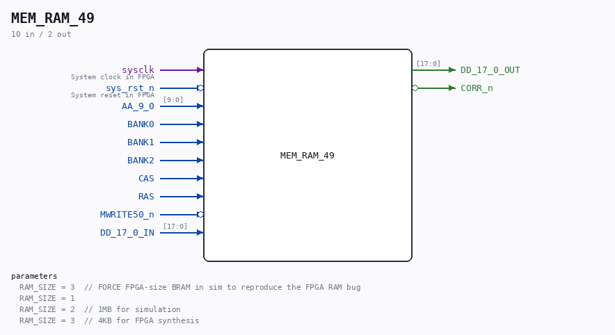
Schematic
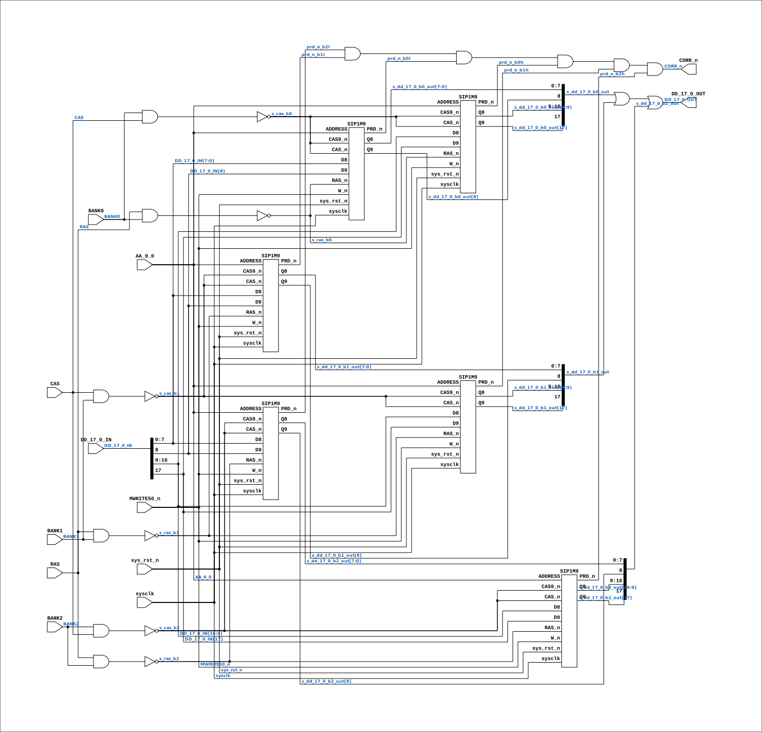
Drawn from the Verilog: no build top uses this module, so it was elaborated from its own file with no defines and default parameters. Sub-modules are boxes (click the picture to open it full size; there every sub-module box links to its page, and every wire shows its Verilog name).
Description
ND120 CPU, MM&M MEM/RAM LOCAL RAM SHEET 49 of 50 Last reviewed: 2-FEB-2025 Ronny Hansen
Parameters
| Parameter | Default |
|---|---|
RAM_SIZE |
3 // FORCE FPGA-size BRAM in sim to reproduce the FPGA RAM bug |
RAM_SIZE |
1 |
RAM_SIZE |
2 // 1MB for simulation |
RAM_SIZE |
3 // 4KB for FPGA synthesis |
Ports
| Direction | Width | Name | Description |
|---|---|---|---|
| input | 1 |
sysclk |
System clock in FPGA |
| input | 1 |
sys_rst_n (active low) |
System reset in FPGA |
| input | [9:0] |
AA_9_0 |
|
| input | 1 |
BANK0 |
|
| input | 1 |
BANK1 |
|
| input | 1 |
BANK2 |
|
| input | 1 |
CAS |
|
| input | 1 |
RAS |
|
| input | 1 |
MWRITE50_n (active low) |
|
| input | [17:0] |
DD_17_0_IN |
|
| output | [17:0] |
DD_17_0_OUT |
|
| output | 1 |
CORR_n (active low) |
Verilog source
Verilog/CPU-BOARD-3202/circuit/MEM_RAM_49.v on GitHub.
Show the Verilog of MEM_RAM_49 (292 lines)
/**************************************************************************
** ND120 CPU, MM&M                                                       **
** MEM/RAM                                                               **
** LOCAL RAM                                                             **
** SHEET 49 of 50                                                        **
**                                                                       **
** Last reviewed: 2-FEB-2025                                             **
** Ronny Hansen                                                          **
***************************************************************************/


// TODO: Add real memory chips, refactor DD_17_0 IN AND OUT signals.
// Or even better, refactor to use one continious RAM in FPGA chip, and use BANK bits as a way to select which bank to use.
// Alternative: Use BLOCK ram to give 64KB/128KB - enough to run test code.

module MEM_RAM_49 #(
    // RAM size configuration: 0=disabled, 1=64KB, 2=1MB, 3=4KB
    // Default to 3 (4KB) for FPGA synthesis, override to 2 (1MB) for Verilator
`ifdef VERILATOR_SIM
  `ifdef FORCE_SMALL_RAM
    parameter integer RAM_SIZE = 3  // FORCE FPGA-size BRAM in sim to reproduce the FPGA RAM bug
  `elsif ND120_SIM_RAM_64K
    // 64K words per chip. Added 29-AUG-2026 so the TPE test programs can be
    // run in Verilator in a bearable time: TPE initialises ALL memory before
    // RUN, one progress '>' per bank, and at ~270k sim cycles/s the 1M-word
    // default takes hours. The cache diagnostic needs very little memory.
    // Build with EXTRA_VDEFINES="-DND120_SIM_RAM_64K" (runSim Makefile).
    parameter integer RAM_SIZE = 1
  `else
    parameter integer RAM_SIZE = 2  // 1MB for simulation
  `endif
`else
    parameter integer RAM_SIZE = 3  // 4KB for FPGA synthesis
`endif
)(

    // Input signals
    input sysclk,    // System clock in FPGA
    input sys_rst_n, // System reset in FPGA

    input [9:0] AA_9_0,
    input       BANK0,
    input       BANK1,
    input       BANK2,

    input CAS,
    input RAS,

    input MWRITE50_n,

    // IN and OUT signals
    input  [17:0] DD_17_0_IN,
    output [17:0] DD_17_0_OUT,

    // Output signals
    output CORR_n
);


  /*******************************************************************************
   ** The wires are defined here                                                 **
   *******************************************************************************/

  wire [ 9:0] s_address;
  wire        s_ras;
  wire        s_cas;
  wire        s_mwrite50_n;
  wire [17:0] s_dd_17_0_in;  // common input signals


  // output
  wire [17:0] s_dd_17_0_out;  // shared output signal depending on bank
  wire        s_corr_n;

  // BANK0
  wire [17:0] s_dd_17_0_b0_out;  // DD out from bank 0
  wire        s_bank0;
  wire        s_ras_b0;
  wire        s_cas_b0;

  wire        prd_n_b0l;
  wire        prd_n_b0h;


  // BANK1
  wire [17:0] s_dd_17_0_b1_out;  // DD out from bank 1
  wire        s_bank1;
  wire        s_ras_b1;
  wire        s_cas_b1;

  wire        prd_n_b1l;
  wire        prd_n_b1h;

  // BANK2
  wire [17:0] s_dd_17_0_b2_out;  // DD out from bank 2
  wire        s_bank2;
  wire        s_ras_b2;
  wire        s_cas_b2;

  wire        prd_n_b2l;
  wire        prd_n_b2h;


  /*******************************************************************************
   ** The module functionality is described here                                 **
   *******************************************************************************/

  /*******************************************************************************
   ** Here all input connections are defined                                     **
   *******************************************************************************/
  assign s_address[9:0] = AA_9_0;

  assign s_bank0 = BANK0;
  assign s_bank2 = BANK2;
  assign s_bank1 = BANK1;

  assign s_ras = RAS;
  assign s_cas = CAS;

  assign s_mwrite50_n = MWRITE50_n;
  assign s_dd_17_0_in = DD_17_0_IN;

  /*******************************************************************************
   ** Here all output connections are defined                                    **
   *******************************************************************************/
  assign CORR_n = s_corr_n;
  assign DD_17_0_OUT = s_dd_17_0_out[17:0];

  /*******************************************************************************
   ** Here all normal components are defined                                     **
   *******************************************************************************/

  // or together all 3 banks
  assign s_dd_17_0_out = s_dd_17_0_b0_out | s_dd_17_0_b1_out | s_dd_17_0_b2_out;

  assign s_ras_b0 = ~(s_ras & s_bank0);
  assign s_cas_b0 = ~(s_bank0 & s_cas);


  assign s_ras_b1 = ~(s_ras & s_bank1);
  assign s_cas_b1 = ~(s_cas & s_bank1);

  assign s_ras_b2 = ~(s_ras & s_bank2);
  assign s_cas_b2 = ~(s_bank2 & s_cas);

  // Calculate CORR ? (in the doc for these RAM chips it seems this pin is not connected..)
  assign s_corr_n = (prd_n_b2l & prd_n_b1l & prd_n_b0l & prd_n_b0h & prd_n_b1h & prd_n_b2h);

  /*******************************************************************************
   ** Here all sub-circuits are defined                                          **
   *******************************************************************************/

  // **************** BANK 0 ****************

// TODO: Make the ram size definition working based on FPGA board.
// Configure RAM size for 3202D board.
// .ramSize: 0=disabled, 1=64KWord, 2=1Mword, 3=4KWord
//
// Note: There seems to be some problems detecting correct RAMSIZE as there is no INRQ defined for undefined RAM.
// Maybe the solution is to trigger RAM parity error..
//
// VIVADO FIX: Use RAM_SIZE parameter (default 3=4KB for FPGA, 2=1MB for Verilator)
// 6MB exceeds device BRAM capacity for synthesis.
// For production with external memory, use RAM_SIZE=2.

  localparam integer RamSize = RAM_SIZE;  // Use parameter: 3 (4KB) for FPGA, 2 (1MB) for Verilator

  SIP1M9  #(.ramSize(RamSize)) CHIP_15H
  (
    .sysclk(sysclk),
    .sys_rst_n(sys_rst_n),

    .ADDRESS(s_address[9:0]),
    .CAS9_n (s_cas_b0),
    .CAS_n  (s_cas_b0),
    .RAS_n  (s_ras_b0),

    .D8(s_dd_17_0_in[7:0]),
    .Q8(s_dd_17_0_b0_out[7:0]),
    .PRD_n(prd_n_b0l),

    .D9(s_dd_17_0_in[8]),
    .Q9(s_dd_17_0_b0_out[8]),

    .W_n(s_mwrite50_n)
  );

  SIP1M9 #(.ramSize(RamSize)) CHIP_15J (
      .sysclk(sysclk),
      .sys_rst_n(sys_rst_n),

      .ADDRESS(s_address[9:0]),
      .CAS9_n (s_cas_b0),
      .CAS_n  (s_cas_b0),
      .RAS_n  (s_ras_b0),

      .D8(s_dd_17_0_in[16:9]),
      .Q8(s_dd_17_0_b0_out[16:9]),
      .PRD_n(prd_n_b0h),

      .D9(s_dd_17_0_in[17]),
      .Q9(s_dd_17_0_b0_out[17]),

      .W_n(s_mwrite50_n)
  );

  // **************** BANK 1 ****************

  SIP1M9 #(.ramSize(RamSize)) CHIP_15K (
      .sysclk(sysclk),
      .sys_rst_n(sys_rst_n),

      .ADDRESS(s_address[9:0]),
      .CAS9_n (s_cas_b1),
      .CAS_n  (s_cas_b1),
      .RAS_n  (s_ras_b1),

      .D8(s_dd_17_0_in[7:0]),
      .Q8(s_dd_17_0_b1_out[7:0]),
      .PRD_n(prd_n_b1l),

      .D9(s_dd_17_0_in[8]),
      .Q9(s_dd_17_0_b1_out[8]),

      .W_n(s_mwrite50_n)
  );

  SIP1M9 #(.ramSize(RamSize)) CHIP_15L (
      .sysclk(sysclk),
      .sys_rst_n(sys_rst_n),

      .ADDRESS(s_address[9:0]),
      .CAS9_n (s_cas_b1),
      .CAS_n  (s_cas_b1),
      .RAS_n  (s_ras_b1),

      .D8(s_dd_17_0_in[16:9]),
      .Q8(s_dd_17_0_b1_out[16:9]),

      .PRD_n(prd_n_b1h),
      .D9(s_dd_17_0_in[17]),
      .Q9(s_dd_17_0_b1_out[17]),

      .W_n(s_mwrite50_n)
  );


  // **************** BANK 2 ****************

  SIP1M9 #(.ramSize(RamSize)) CHIP_15M (
      .sysclk(sysclk),
      .sys_rst_n(sys_rst_n),

      .ADDRESS(s_address[9:0]),
      .CAS9_n (s_cas_b2),
      .CAS_n  (s_cas_b2),
      .RAS_n  (s_ras_b2),

      .D8(s_dd_17_0_in[7:0]),
      .Q8(s_dd_17_0_b2_out[7:0]),

      .PRD_n(prd_n_b2l),
      .D9(s_dd_17_0_in[8]),
      .Q9(s_dd_17_0_b2_out[8]),

      .W_n(s_mwrite50_n)
  );


  SIP1M9 #(.ramSize(RamSize)) CHIP_15N (
      .sysclk(sysclk),
      .sys_rst_n(sys_rst_n),

      .ADDRESS(s_address[9:0]),
      .CAS9_n (s_cas_b2),
      .CAS_n  (s_cas_b2),
      .RAS_n  (s_ras_b2),

      .D8(s_dd_17_0_in[16:9]),
      .Q8(s_dd_17_0_b2_out[16:9]),

      .PRD_n(prd_n_b2h),
      .D9(s_dd_17_0_in[17]),
      .Q9(s_dd_17_0_b2_out[17]),

      .W_n(s_mwrite50_n)
  );


endmodule