BIF_BCTL_6
Source: Verilog/CPU-BOARD-3202/circuit/BIF_BCTL_6.v
Where it sits (Simulation): ND120_TOP > ND120_CORE > ND3202D > BIF_5 > BIF_BCTL_6
- instance path: CORE.CPU_BOARD.BIF.BCTL
Used in: BIF_5 (all tops)
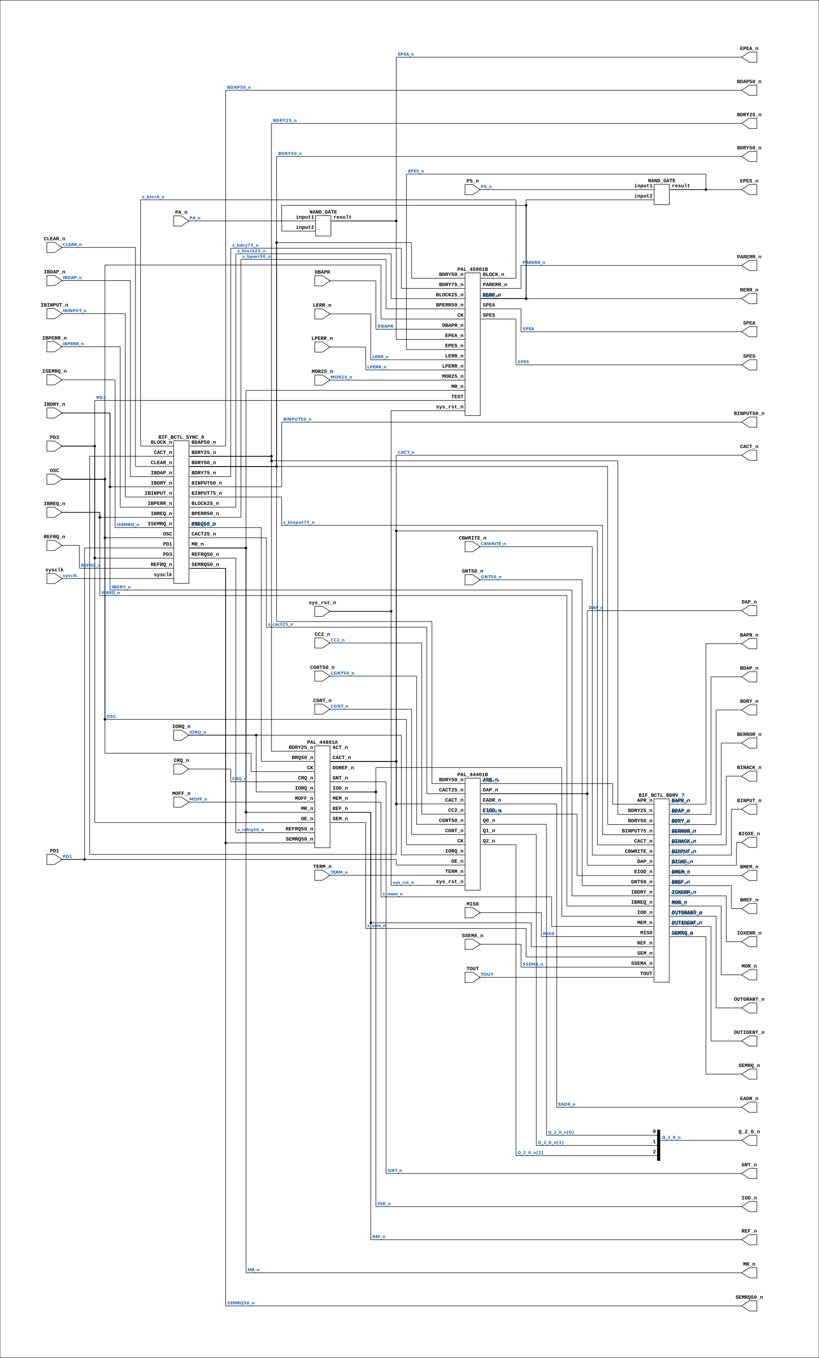
Contains: BIF_BCTL_BDRV_7, BIF_BCTL_SYNC_8, NAND_GATE x2, PAL_44401B, PAL_44801A, PAL_45001B
Module hierarchy - All modules
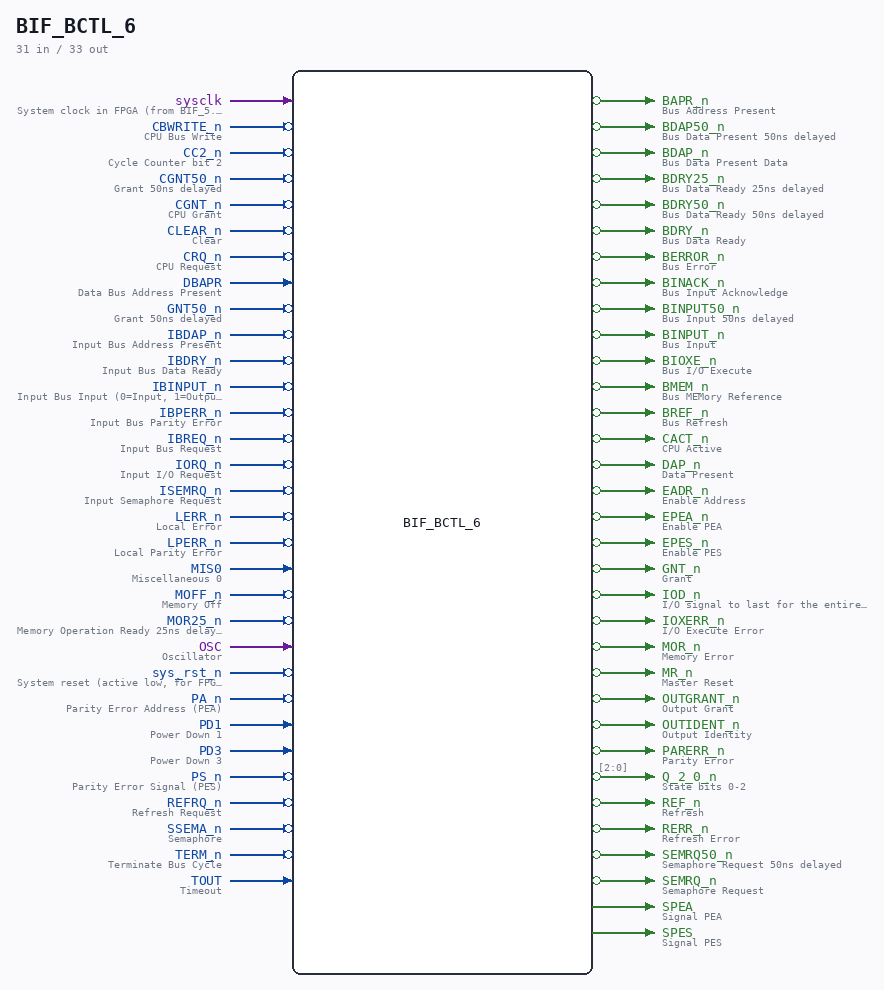
Schematic
Drawn from the Verilog: the yosys netlist of the Simulation (Verilator) build, instance CORE.CPU_BOARD.BIF.BCTL. Sub-modules are boxes (click the picture to open it full size; there every sub-module box links to its page, and every wire shows its Verilog name).
Description
ND120 CPU, MM&M BIF/BCTL BIF CONTROL SHEET 6 of 50 Last reviewed: 22-MAR-2025 Ronny Hansen
Ports
| Direction | Width | Name | Description |
|---|---|---|---|
| input | 1 |
sysclk |
System clock in FPGA (from BIF_5.sysclk) |
| input | 1 |
CBWRITE_n (active low) |
CPU Bus Write |
| input | 1 |
CC2_n (active low) |
Cycle Counter bit 2 |
| input | 1 |
CGNT50_n (active low) |
Grant 50ns delayed |
| input | 1 |
CGNT_n (active low) |
CPU Grant |
| input | 1 |
CLEAR_n (active low) |
Clear |
| input | 1 |
CRQ_n (active low) |
CPU Request |
| input | 1 |
DBAPR |
Data Bus Address Present |
| input | 1 |
GNT50_n (active low) |
Grant 50ns delayed |
| input | 1 |
IBDAP_n (active low) |
Input Bus Address Present |
| input | 1 |
IBDRY_n (active low) |
Input Bus Data Ready |
| input | 1 |
IBINPUT_n (active low) |
Input Bus Input (0=Input, 1=Output) |
| input | 1 |
IBPERR_n (active low) |
Input Bus Parity Error |
| input | 1 |
IBREQ_n (active low) |
Input Bus Request |
| input | 1 |
IORQ_n (active low) |
Input I/O Request |
| input | 1 |
ISEMRQ_n (active low) |
Input Semaphore Request |
| input | 1 |
LERR_n (active low) |
Local Error |
| input | 1 |
LPERR_n (active low) |
Local Parity Error |
| input | 1 |
MIS0 |
Miscellaneous 0 |
| input | 1 |
MOFF_n (active low) |
Memory Off |
| input | 1 |
MOR25_n (active low) |
Memory Operation Ready 25ns delayed |
| input | 1 |
OSC |
Oscillator |
| input | 1 |
sys_rst_n (active low) |
System reset (active low, for FPGA synthesis) |
| input | 1 |
PA_n (active low) |
Parity Error Address (PEA) |
| input | 1 |
PD1 |
Power Down 1 |
| input | 1 |
PD3 |
Power Down 3 |
| input | 1 |
PS_n (active low) |
Parity Error Signal (PES) |
| input | 1 |
REFRQ_n (active low) |
Refresh Request |
| input | 1 |
SSEMA_n (active low) |
Semaphore |
| input | 1 |
TERM_n (active low) |
Terminate Bus Cycle |
| input | 1 |
TOUT |
Timeout |
| output | 1 |
BAPR_n (active low) |
Bus Address Present |
| output | 1 |
BDAP50_n (active low) |
Bus Data Present 50ns delayed |
| output | 1 |
BDAP_n (active low) |
Bus Data Present Data |
| output | 1 |
BDRY25_n (active low) |
Bus Data Ready 25ns delayed |
| output | 1 |
BDRY50_n (active low) |
Bus Data Ready 50ns delayed |
| output | 1 |
BDRY_n (active low) |
Bus Data Ready |
| output | 1 |
BERROR_n (active low) |
Bus Error |
| output | 1 |
BINACK_n (active low) |
Bus Input Acknowledge |
| output | 1 |
BINPUT50_n (active low) |
Bus Input 50ns delayed |
| output | 1 |
BINPUT_n (active low) |
Bus Input |
| output | 1 |
BIOXE_n (active low) |
Bus I/O Execute |
| output | 1 |
BMEM_n (active low) |
Bus MEMory Reference |
| output | 1 |
BREF_n (active low) |
Bus Refresh |
| output | 1 |
CACT_n (active low) |
CPU Active |
| output | 1 |
DAP_n (active low) |
Data Present |
| output | 1 |
EADR_n (active low) |
Enable Address |
| output | 1 |
EPEA_n (active low) |
Enable PEA |
| output | 1 |
EPES_n (active low) |
Enable PES |
| output | 1 |
GNT_n (active low) |
Grant |
| output | 1 |
IOD_n (active low) |
I/O signal to last for the entire bus cycle |
| output | 1 |
IOXERR_n (active low) |
I/O Execute Error |
| output | 1 |
MOR_n (active low) |
Memory Error |
| output | 1 |
MR_n (active low) |
Master Reset |
| output | 1 |
OUTGRANT_n (active low) |
Output Grant |
| output | 1 |
OUTIDENT_n (active low) |
Output Identity |
| output | 1 |
PARERR_n (active low) |
Parity Error |
| output | [2:0] |
Q_2_0_n (active low) |
State bits 0-2 |
| output | 1 |
REF_n (active low) |
Refresh |
| output | 1 |
RERR_n (active low) |
Refresh Error |
| output | 1 |
SEMRQ50_n (active low) |
Semaphore Request 50ns delayed |
| output | 1 |
SEMRQ_n (active low) |
Semaphore Request |
| output | 1 |
SPEA |
Signal PEA |
| output | 1 |
SPES |
Signal PES |
Verilog source
Verilog/CPU-BOARD-3202/circuit/BIF_BCTL_6.v on GitHub.
Show the Verilog of BIF_BCTL_6 (463 lines)
/**************************************************************************
** ND120 CPU, MM&M                                                       **
** BIF/BCTL                                                              **
** BIF CONTROL                                                           **
** SHEET 6 of 50                                                         **
**                                                                       **
** Last reviewed: 22-MAR-2025                                            **
** Ronny Hansen                                                          **
***************************************************************************/

module BIF_BCTL_6 (
    input sysclk,             //! System clock in FPGA (from BIF_5.sysclk)
    input CBWRITE_n,  //! CPU Bus Write
    input CC2_n,      //! Cycle Counter bit 2
    input CGNT50_n,   //! Grant 50ns delayed
    input CGNT_n,     //! CPU Grant
    input CLEAR_n,    //! Clear
    input CRQ_n,      //! CPU Request
    input DBAPR,      //! Data Bus Address Present
    input GNT50_n,    //! Grant 50ns delayed
    input IBDAP_n,    //! Input Bus Address Present
    input IBDRY_n,    //! Input Bus Data Ready
    input IBINPUT_n,  //! Input Bus Input (0=Input, 1=Output)
    input IBPERR_n,   //! Input Bus Parity Error
    input IBREQ_n,    //! Input Bus Request
    input IORQ_n,     //! Input I/O Request
    input ISEMRQ_n,   //! Input Semaphore Request
    input LERR_n,     //! Local Error
    input LPERR_n,    //! Local Parity Error
    input MIS0,       //! Miscellaneous 0
    input MOFF_n,     //! Memory Off
    input MOR25_n,    //! Memory Operation Ready 25ns delayed
    input OSC,        //! Oscillator
    input sys_rst_n,  //! System reset (active low, for FPGA synthesis)
    input PA_n,       //! Parity Error Address (PEA)
    input PD1,        //! Power Down 1
    input PD3,        //! Power Down 3
    input PS_n,       //! Parity Error Signal (PES)
    input REFRQ_n,    //! Refresh Request
    input SSEMA_n,    //! Semaphore
    input TERM_n,     //! Terminate Bus Cycle
    input TOUT,       //! Timeout

    output       BAPR_n,      //! Bus Address Present
    output       BDAP50_n,    //! Bus Data Present 50ns delayed
    output       BDAP_n,      //! Bus Data Present Data
    output       BDRY25_n,    //! Bus Data Ready 25ns delayed
    output       BDRY50_n,    //! Bus Data Ready 50ns delayed
    output       BDRY_n,      //! Bus Data Ready
    output       BERROR_n,    //! Bus Error
    output       BINACK_n,    //! Bus Input Acknowledge
    output       BINPUT50_n,  //! Bus Input 50ns delayed
    output       BINPUT_n,    //! Bus Input
    output       BIOXE_n,     //! Bus I/O Execute
    output       BMEM_n,      //! Bus MEMory Reference
    output       BREF_n,      //! Bus Refresh
    output       CACT_n,      //! CPU Active
    output       DAP_n,       //! Data Present
    output       EADR_n,      //! Enable Address
    output       EPEA_n,      //! Enable PEA
    output       EPES_n,      //! Enable PES
    output       GNT_n,       //! Grant
    output       IOD_n,       //! I/O signal to last for the entire bus cycle
    output       IOXERR_n,    //! I/O Execute Error
    output       MOR_n,       //! Memory Error
    output       MR_n,        //! Master Reset
    output       OUTGRANT_n,  //! Output Grant
    output       OUTIDENT_n,  //! Output Identity
    output       PARERR_n,    //! Parity Error
    output [2:0] Q_2_0_n,     //! State bits 0-2
    output       REF_n,       //! Refresh
    output       RERR_n,      //! Refresh Error
    output       SEMRQ50_n,   //! Semaphore Request 50ns delayed
    output       SEMRQ_n,     //! Semaphore Request
    output       SPEA,        //! Signal PEA
    output       SPES         //! Signal PES
);

  /*******************************************************************************
   ** The wires are defined here                                                 **
   *******************************************************************************/
  wire [2:0] s_q_2_0_n;
  wire       s_term_n;
  wire       s_moff_n;
  wire       s_pd1;
  wire       s_iorq_n;
  wire       s_dbapr;
  wire       s_clear_n;
  wire       s_ibdap_n;
  wire       s_ibperr_n;
  wire       s_ibreq_n;
  wire       s_gnt50_n;
  wire       s_ibdry_n;
  wire       s_cc2_n;
  wire       s_cgnt_n;
  wire       s_mor25_n;
  wire       s_refrq_n;
  wire       s_crq_n;
  wire       s_tout;
  wire       s_ibinput_n;
  wire       s_ps_n;
  wire       s_cgnt50_n;
  wire       s_lperr_n;
  wire       s_isemrq_n;
  wire       s_ssema_n;
  wire       s_pa_n;
  wire       s_osc;
  wire       s_lerr_n;
  wire       s_mis0;
  wire       s_pd3;
  wire       s_cbwrite_n;
  wire       s_bdry50_n;
  wire       s_apr_n;
  wire       s_bapr_n;
  wire       s_bdap50_n;
  wire       s_bdap_n;
  wire       s_bdry25_n;
  wire       s_bdry_n;
  wire       s_berror_n;
  wire       s_binack_n;
  wire       s_binput50_n;
  wire       s_binput_n;
  wire       s_bioxe_n;
  wire       s_bmem_n;
  wire       s_bref_n;
  wire       s_cact_n;
  wire       s_dap_n;
  wire       s_eadr_n;
  wire       s_epea_n;
  wire       s_epes_n;
  wire       s_gnt_n;
  wire       s_iod_n;
  wire       s_ioxerr_n;
  wire       s_mor_n;
  wire       s_mr_n;
  wire       s_outgrant_n;
  wire       s_outident_n;
  wire       s_parerr_n;
  wire       s_ref_n;
  wire       s_rerr_n;
  wire       s_semrq50_n;
  wire       s_semrq_n;
  wire       s_spea;
  wire       s_spes;
  wire       s_binput75_n;
  wire       s_block_n;
  wire       s_bperr50_n;
  wire       s_block25_n;
  wire       s_bdry75_n;
  wire       s_mem_n;
  wire       s_cact25_n;
  wire       s_eiod_n;
  wire       s_brq50_n;
  wire       s_refrq50_n;
  wire       s_sem_n;

  /*******************************************************************************
   ** Here all input connections are defined                                     **
   *******************************************************************************/
  assign s_term_n    = TERM_n;
  assign s_moff_n    = MOFF_n;
  assign s_pd1       = PD1;
  assign s_iorq_n    = IORQ_n;
  assign s_dbapr     = DBAPR;
  assign s_clear_n   = CLEAR_n;
  assign s_ibdap_n   = IBDAP_n;
  assign s_ibperr_n  = IBPERR_n;
  assign s_ibreq_n   = IBREQ_n;
  assign s_gnt50_n   = GNT50_n;
  assign s_ibdry_n   = IBDRY_n;
  assign s_cc2_n     = CC2_n;
  assign s_cgnt_n    = CGNT_n;
  assign s_mor25_n   = MOR25_n;
  assign s_refrq_n   = REFRQ_n;
  assign s_crq_n     = CRQ_n;
  assign s_tout      = TOUT;
  assign s_ibinput_n = IBINPUT_n;
  assign s_ps_n      = PS_n;
  assign s_cgnt50_n  = CGNT50_n;
  assign s_lperr_n   = LPERR_n;
  assign s_isemrq_n  = ISEMRQ_n;
  assign s_ssema_n   = SSEMA_n;
  assign s_pa_n      = PA_n;
  assign s_osc       = OSC;
  assign s_lerr_n    = LERR_n;
  assign s_mis0      = MIS0;
  assign s_pd3       = PD3;
  assign s_cbwrite_n = CBWRITE_n;

  /*******************************************************************************
   ** Here all output connections are defined                                    **
   *******************************************************************************/
  assign BAPR_n      = s_bapr_n;
  assign BDAP50_n    = s_bdap50_n;
  assign BDAP_n      = s_bdap_n;
  assign BDRY25_n    = s_bdry25_n;
  assign BDRY50_n    = s_bdry50_n;
  assign BDRY_n      = s_bdry_n;
  assign BERROR_n    = s_berror_n;
  assign BINACK_n    = s_binack_n;
  assign BINPUT50_n  = s_binput50_n;
  assign BINPUT_n    = s_binput_n;
  assign BIOXE_n     = s_bioxe_n;
  assign BMEM_n      = s_bmem_n;
  assign BREF_n      = s_bref_n;
  assign CACT_n      = s_cact_n;
  assign DAP_n       = s_dap_n;
  assign EADR_n      = s_eadr_n;
  assign EPEA_n      = s_epea_n;
  assign EPES_n      = s_epes_n;
  assign GNT_n       = s_gnt_n;
  assign IOD_n       = s_iod_n;
  assign IOXERR_n    = s_ioxerr_n;
  assign MOR_n       = s_mor_n;
  assign MR_n        = s_mr_n;  //! Master Reset (negated)
  assign OUTGRANT_n  = s_outgrant_n;
  assign OUTIDENT_n  = s_outident_n;
  assign PARERR_n    = s_parerr_n;
  assign Q_2_0_n     = s_q_2_0_n[2:0];
  assign REF_n       = s_ref_n;
  assign RERR_n      = s_rerr_n;
  assign SEMRQ50_n   = s_semrq50_n;
  assign SEMRQ_n     = s_semrq_n;
  assign SPEA        = s_spea;
  assign SPES        = s_spes;

  /*******************************************************************************
   ** Here all normal components are defined                                     **
   *******************************************************************************/
  NAND_GATE #(
      .BubblesMask(2'b11)
  ) GATES_1 (
      .input1(s_ps_n),
      .input2(s_rerr_n),
      .result(s_epes_n)
  );

  NAND_GATE #(
      .BubblesMask(2'b11)
  ) GATES_2 (
      .input1(s_pa_n),
      .input2(s_rerr_n),
      .result(s_epea_n)
  );

  /*******************************************************************************
   ** Here all sub-circuits are defined                                          **
   *******************************************************************************/

  /*
   * Bus arbitration PAL for the ND120 CPU system.
   * Handles arbitration between CPU requests, I/O requests, refresh requests, and semaphore requests.
   * Takes inputs like CPU request (CRQ_n), I/O request (IORQ_n), bus request (BRQ50_n), refresh request (REFRQ50_n),
   * and semaphore request (SEMRQ50_n) to generate appropriate grant and control signals.
   * Outputs include semaphore control (SEM_n), refresh control (REF_n), I/O data control (IOD_n),
   * bus grant (GNT_n) and CPU active (CACT_n) signals to coordinate bus access.
   * Uses a clock input (CK) and output enable (OE_n) to control timing of state changes.
   */
  PAL_44801A PAL_44801_UBARB (
      .CK  (s_osc),  // Clock signal
      .OE_n(s_pd3),  // OUTPUT ENABLE (active-low) for Q0-Q5

      .CRQ_n    (s_crq_n),      // I0 - CRQ_n
      .IORQ_n   (s_iorq_n),     // I1 - IORQ_n
      .MR_n     (s_mr_n),       // I2 - MR_n
      .BRQ50_n  (s_brq50_n),    // I3 - BRQ50_n
      .REFRQ50_n(s_refrq50_n),  // I4 - REFRQ50_n
      .BDRY25_n (s_bdry25_n),   // I5 - BDRY25_n
      .SEMRQ50_n(s_semrq50_n),  // I6 - SEMRQ50_n
      .MOFF_n   (s_moff_n),     // I7 - MOFF_n

      .SEM_n  (s_sem_n),   // Q0_n - SEM_n
      .ACT_n  (),          // Q1_n - ACT_n (n.c.)
      .DOREF_n(),          // Q2_n - DOREF_n (n.c.)
      .MEM_n  (s_mem_n),   // Q3_n - MEM_n
      .REF_n  (s_ref_n),   // Q4_n - REF_n
      .IOD_n  (s_iod_n),   // Q5_n - IOD_n
      .GNT_n  (s_gnt_n),   // Q6_n - GNT_n
      .CACT_n (s_cact_n)   // Q7_n - CACT_n
  );

  /*
   * Bus timing control PAL for the ND120 CPU system.
   * Manages bus cycle timing and control signal generation based on CPU activity,
   * bus data ready, and grant signals. Generates state bits (Q0-Q2) to track bus
   * cycle phases and control signals for address present (APR_n), data present (DAP_n),
   * I/O data enable (EIOD_n) and address enable (EADR_n). Uses delayed versions of
   * control signals (CACT25_n, BDRY50_n, CGNT50_n) for proper timing relationships.
   */
  PAL_44401B PAL_44401_UBTIM (
      .CK  (s_osc),
      .sys_rst_n(sys_rst_n),
      .OE_n(s_pd1),

      .CC2_n   (s_cc2_n),     // I0
      .CACT_n  (s_cact_n),    // I1
      .CACT25_n(s_cact25_n),  // I2
      .BDRY50_n(s_bdry50_n),  // I3
      .CGNT_n  (s_cgnt_n),    // I4
      .CGNT50_n(s_cgnt50_n),  // I5
      .TERM_n  (s_term_n),    // I6
      .IORQ_n  (s_iorq_n),    // I7

      .Q0_n(s_q_2_0_n[0]),  // Q0_n
      .Q1_n(s_q_2_0_n[1]),  // Q1_n
      .Q2_n(s_q_2_0_n[2]),  // Q2_n
      //.Q3_n(),                 // Q3_n (not connected, no signal)

      .APR_n (s_apr_n),   // B0_n
      .DAP_n (s_dap_n),   // B1_n
      .EIOD_n(s_eiod_n),  // B2_n
      .EADR_n(s_eadr_n)   // B3_n
  );

  /*
   * Bus parity and error handling PAL for the ND120 CPU system.
   * Monitors bus timing signals and error conditions to detect parity errors
   * and other faults during data transfers. Generates error signals (PARERR_n, RERR_n)
   * and control signals (SPEA, SPES) to handle error conditions. Also provides
   * bus blocking capability (BLOCK_n) and local error reporting (LERR_n).
   * Includes test functionality and interfaces with memory operation ready signals.
   */
  PAL_45001B PAL_45001_UBPAR (
      .CK       (s_osc),        // Clock (added for FPGA synthesis)
      .sys_rst_n(sys_rst_n),    // System reset (for FPGA synthesis)

      .BDRY50_n (s_bdry50_n),   // I0 - BDRY50_n Bus Data Ready 50ns delayed
      .BDRY75_n (s_bdry75_n),   // I1 - BDRY75_n Bus Data Ready 75ns delayed
      .BLOCK25_n(s_block25_n),  // I2 - BLOCK25_n Block 25ns delayed
      .BPERR50_n(s_bperr50_n),  // I3 - BPERR50_n Bus Parity Error 50ns delayed
      .DBAPR_n  (s_dbapr),      // I4 - DBAPR_n Data Bus Address Present (input)
      .MOR25_n  (s_mor25_n),    // I5 - MOR25_n Memory Error 25ns delayed
      .LPERR_n  (s_lperr_n),    // I6 - LPERR_n Local Parity Error
      .MR_n     (s_mr_n),       // I7 - MR_n Master Reset
      .EPES_n   (s_epes_n),     // I8 - EPES_n Enable Parity Error Status Word (read)
      .EPEA_n   (s_epea_n),     // I9 - EPEA_n Enable Parity Error Address (read)

      .SPEA(s_spea),  // Y0_n (OUT Only) Strobe Parity Error Address (PEA) (write)
      .SPES(s_spes),  // Y1_n (OUT ONLY) Strobe Parity Error Status Word (PES) (write)

      .BLOCK_n (s_block_n),   // B0_n - BLOCK_n (out) Block signal for PES and PEA strobe
      .PARERR_n(s_parerr_n),  // B1_n - PARERR_n (out) Parity Error signal from bus and local memory
      .RERR_n  (s_rerr_n),    // B2_n - RERR_n (out) Refresh Error signal
      //.B3_n(),              // B3_n - (n.c.)
      .TEST    (s_pd3),       // B4_n - TEST
      .LERR_n  (s_lerr_n)     // B5_n - LERR_n (out) Local Error signal
  );

`ifdef PESDBG
  // Issue-F probe (inert unless -DPESDBG): log every change on the SLOW links
  // of the PES/PEA capture-freeze-readback chain around PAL 45001B (freeze,
  // error latches, readback strobes), plus pulse COUNTS for the fast SPEA/SPES
  // capture strobes, to find which link stays dead during PAGING test 11
  // (PES/PEA read back 0). Counts keep the log under the size cap - SPEA fires
  // every bus cycle by design after the strobe fix.
  reg [8:0] r_pesdbg_d = 9'b111111111;
  reg r_spea_d = 1'b0, r_spes_d = 1'b0;
  reg [31:0] r_spea_cnt = 0, r_spes_cnt = 0;
  wire [8:0] s_pesdbg_now = {s_rerr_n, s_block_n, s_mor25_n, s_ps_n, s_pa_n,
                             s_epes_n, s_epea_n, s_parerr_n, s_lerr_n};
  always @(posedge s_osc) begin
    if (s_spea && !r_spea_d) r_spea_cnt <= r_spea_cnt + 1;
    if (s_spes && !r_spes_d) r_spes_cnt <= r_spes_cnt + 1;
    r_spea_d <= s_spea;
    r_spes_d <= s_spes;
    if (s_pesdbg_now != r_pesdbg_d)
      $display("[pes] rerr_n=%b block_n=%b mor25_n=%b ps_n=%b pa_n=%b epes_n=%b epea_n=%b parerr_n=%b lerr_n=%b speaN=%0d spesN=%0d",
               s_rerr_n, s_block_n, s_mor25_n, s_ps_n, s_pa_n,
               s_epes_n, s_epea_n, s_parerr_n, s_lerr_n, r_spea_cnt, r_spes_cnt);
    r_pesdbg_d <= s_pesdbg_now;
  end
`endif


  /*
   * Bus driver module for the ND120 CPU bus interface.
   * Handles bus signal generation and timing for data transfers.
   * Takes various control signals like address present, CPU active, and memory signals
   * as inputs to generate properly timed bus control signals.
   * Manages bus handshaking through data ready/present signals, handles I/O operations,
   * memory access, semaphore requests, and error conditions.
   * Provides multiple delayed versions of key signals for proper bus timing.
   */
  BIF_BCTL_BDRV_7 BDRV (
      // Input signals
      .APR_n      (s_apr_n),      // Address Present
      .BDRY25_n   (s_bdry25_n),   // Bus Data Ready (25ns delayed)
      .BDRY50_n   (s_bdry50_n),   // Bus Data Ready (50ns delayed)
      .BINPUT75_n (s_binput75_n), // Bus Input (75ns delayed)
      .CACT_n     (s_cact_n),     // CPU Active
      .CBWRITE_n  (s_cbwrite_n),  // CPU Bus Write
      .DAP_n      (s_dap_n),      // Data Present
      .EIOD_n     (s_eiod_n),     // Enable I/O Data
      .GNT50_n    (s_gnt50_n),    // Grant (50ns delayed)
      .IBDRY_n    (s_ibdry_n),    // Input Bus Data Ready
      .IBREQ_n    (s_ibreq_n),    // Input Bus Request
      .IOD_n      (s_iod_n),      // IO D signal
      .MEM_n      (s_mem_n),      // Memory
      .MIS0       (s_mis0),       // Microcode Misc 0 bit
      .REF_n      (s_ref_n),      // Refresh
      .SEM_n      (s_sem_n),      // Semaphore
      .SSEMA_n    (s_ssema_n),    // Semaphore
      .TOUT       (s_tout),       // Timeout

      // Output signals
      .BAPR_n     (s_bapr_n),      // Bus Address Present
      .BDAP_n     (s_bdap_n),      // Bus Data Present
      .BDRY_n     (s_bdry_n),      // Bus Data Ready
      .BERROR_n   (s_berror_n),    // Bus Error
      .BINACK_n   (s_binack_n),    // Bus Input Acknowledge
      .BINPUT_n   (s_binput_n),    // Bus Input
      .BIOXE_n    (s_bioxe_n),     // Bus I/O Execute
      .BMEM_n     (s_bmem_n),      // Bus Memory
      .BREF_n     (s_bref_n),      // Bus Refresh
      .IOXERR_n   (s_ioxerr_n),    // I/O Execute Error
      .MOR_n      (s_mor_n),       // Memory Error
      .OUTGRANT_n (s_outgrant_n),  // Output Grant
      .OUTIDENT_n (s_outident_n),  // Output Identify
      .SEMRQ_n    (s_semrq_n)      // Semaphore Request
  );


  /*
   * Synchronization module for the ND120 CPU bus interface.
   * Handles timing and synchronization of various bus control signals.
   * Generates delayed versions of key bus signals (25ns, 50ns, 75ns)
   * for proper bus timing and handshaking.
   * Also handles reset, refresh and CPU active signal synchronization.
   */
  BIF_BCTL_SYNC_8 SYNC (
      .sysclk(sysclk),
      // Inputs
      .CLEAR_n  (s_clear_n),    // Clear signal
      .IBDAP_n  (s_ibdap_n),    // Input Bus Data Present
      .IBDRY_n  (s_ibdry_n),    // Input Bus Data Ready
      .IBINPUT_n(s_ibinput_n),  // Input Bus Input
      .IBPERR_n (s_ibperr_n),   // Input Bus Parity Error
      .IBREQ_n  (s_ibreq_n),    // Input Bus Request
      .ISEMRQ_n (s_isemrq_n),   // Input Semaphore Request
      .MR_n     (s_mr_n),       // Master Reset
      .OSC      (s_osc),        // Oscillator
      .PD1      (s_pd1),        // Pull-down 1
      .PD3      (s_pd3),        // Pull-down 3
      .REFRQ_n  (s_refrq_n),    // Refresh Request

      // Outputs
      .BDAP50_n  (s_bdap50_n),    // Bus Data Present (50ns delayed)
      .BDRY25_n  (s_bdry25_n),    // Bus Data Ready (25ns delayed)
      .BDRY50_n  (s_bdry50_n),    // Bus Data Ready (50ns delayed)
      .BDRY75_n  (s_bdry75_n),    // Bus Data Ready (75ns delayed)
      .BINPUT50_n(s_binput50_n),  // Bus Input (50ns delayed)
      .BINPUT75_n(s_binput75_n),  // Bus Input (75ns delayed)
      .BLOCK25_n (s_block25_n),   // Block (25ns delayed)
      .BLOCK_n   (s_block_n),     // Block
      .BPERR50_n (s_bperr50_n),   // Bus Parity Error (50ns delayed)
      .BREQ50_n  (s_brq50_n),     // Bus Request (50ns delayed)
      .CACT25_n  (s_cact25_n),    // CPU Active (25ns delayed)
      .CACT_n    (s_cact_n),      // CPU Active
      .REFRQ50_n (s_refrq50_n),   // Refresh Request (50ns delayed)
      .SEMRQ50_n (s_semrq50_n)    // Semaphore Request (50ns delayed)
  );

endmodule