PAL_45001B
Source: Verilog/PAL/PAL_45001B.v
Where it sits (Simulation): ND120_TOP > ND120_CORE > ND3202D > BIF_5 > BIF_BCTL_6 > PAL_45001B
- instance path: CORE.CPU_BOARD.BIF.BCTL.PAL_45001_UBPAR
Used in: BIF_BCTL_6 (all tops)
Contains: no other modules.
Module hierarchy - All modules
Schematic
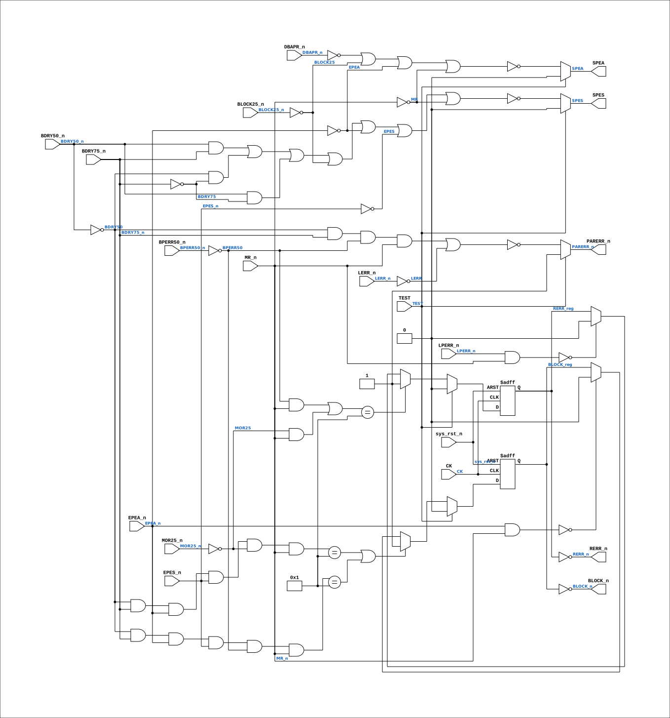
Drawn from the Verilog: the yosys netlist of the Simulation (Verilator) build, instance CORE.CPU_BOARD.BIF.BCTL.PAL_45001_UBPAR. Sub-modules are boxes (click the picture to open it full size; there every sub-module box links to its page, and every wire shows its Verilog name).
Description
ND120 PALASM CODE CONVERTED TO VERILOG Component PAL 45001B Last reviewed: 14-DEC-2024 Ronny Hansen
Ports
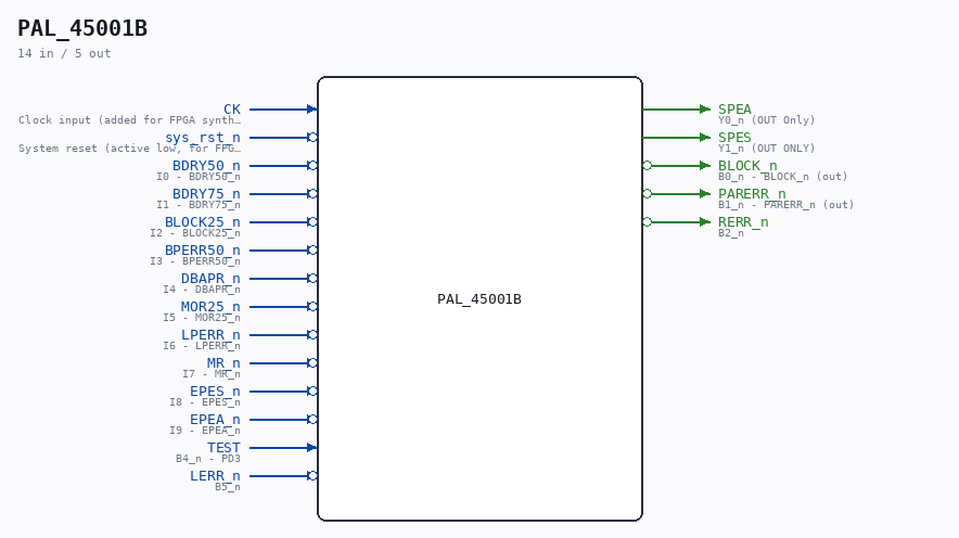
| Direction | Width | Name | Description |
|---|---|---|---|
| input | 1 |
CK |
Clock input (added for FPGA synthesis) |
| input | 1 |
sys_rst_n (active low) |
System reset (active low, for FPGA synthesis) |
| input | 1 |
BDRY50_n (active low) |
I0 - BDRY50_n |
| input | 1 |
BDRY75_n (active low) |
I1 - BDRY75_n |
| input | 1 |
BLOCK25_n (active low) |
I2 - BLOCK25_n |
| input | 1 |
BPERR50_n (active low) |
I3 - BPERR50_n |
| input | 1 |
DBAPR_n (active low) |
I4 - DBAPR_n |
| input | 1 |
MOR25_n (active low) |
I5 - MOR25_n |
| input | 1 |
LPERR_n (active low) |
I6 - LPERR_n |
| input | 1 |
MR_n (active low) |
I7 - MR_n |
| input | 1 |
EPES_n (active low) |
I8 - EPES_n |
| input | 1 |
EPEA_n (active low) |
I9 - EPEA_n |
| output | 1 |
SPEA |
Y0_n (OUT Only) |
| output | 1 |
SPES |
Y1_n (OUT ONLY) |
| output | 1 |
BLOCK_n (active low) |
B0_n - BLOCK_n (out) |
| output | 1 |
PARERR_n (active low) |
B1_n - PARERR_n (out) |
| output | 1 |
RERR_n (active low) |
B2_n |
| input | 1 |
TEST |
B4_n - PD3 |
| input | 1 |
LERR_n (active low) |
B5_n |
Verilog source
Verilog/PAL/PAL_45001B.v on GitHub.
Show the Verilog of PAL_45001B (161 lines)
/**********************************************************************************************************
** ND120 PALASM CODE CONVERTED TO VERILOG                                                                **
**                                                                                                       **
** Component PAL 45001B                                                                                  **
**                                                                                                       **
** Last reviewed: 14-DEC-2024                                                                            **
** Ronny Hansen                                                                                          **
***********************************************************************************************************/

// PAL16L8
// JLB/CJTC 11AUG86
// 45001B, 8D, BPAR

// PCB 3202D sheet 6:
//

// PAL 16L8
// 10 INPUT only pins (I0-I9)
// 2 OUT only pins (Y0-Y1) and 6 IN or OUT pins (B0-B5)
//
// PAL16RL8 (https://rocelec.widen.net/view/pdf/c6dwcslffz/VANTS00080-1.pdf)

// NOTE: PAL16L8 is purely combinational in the original hardware.
// Clock input added for FPGA synthesis to eliminate latch inference.

module PAL_45001B (
    input CK,         //! Clock input (added for FPGA synthesis)
    input sys_rst_n,  //! System reset (active low, for FPGA synthesis)

    input BDRY50_n,   //! I0 - BDRY50_n
    input BDRY75_n,   //! I1 - BDRY75_n
    input BLOCK25_n,  //! I2 - BLOCK25_n
    input BPERR50_n,  //! I3 - BPERR50_n
    input DBAPR_n,    //! I4 - DBAPR_n
    input MOR25_n,    //! I5 - MOR25_n
    input LPERR_n,    //! I6 - LPERR_n
    input MR_n,       //! I7 - MR_n
    input EPES_n,     //! I8 - EPES_n
    input EPEA_n,     //! I9 - EPEA_n


    output SPEA,  //! Y0_n (OUT Only)
    output SPES,  //! Y1_n (OUT ONLY)

    output BLOCK_n,   //! B0_n - BLOCK_n (out)
    output PARERR_n,  //! B1_n - PARERR_n (out)
    output RERR_n,    //! B2_n
    //inout B3_n,     //! B3_n - (n.c.)
    input  TEST,      //! B4_n - PD3
    input  LERR_n     //! B5_n
);


  // Creating non-negated wires for active-low inputs
  wire BDRY50 = ~BDRY50_n;
  wire BDRY75 = ~BDRY75_n;
  wire BLOCK25 = ~BLOCK25_n;
  wire BPERR50 = ~BPERR50_n;
  wire MOR25 = ~MOR25_n;
  wire MR = ~MR_n;
  wire EPES = ~EPES_n;
  wire EPEA = ~EPEA_n;
  wire LERR = ~LERR_n;


  // STROBE PARITY ERROR STATUS WORD
  // PALASM 45001B: /SPES = ... + BLOCK25 + ... - the strobe stops once the
  // BLOCK freeze is ACTIVE. The old BLOCK25_n literal inverted the freeze
  // (SPES could never fire before an error).
  assign SPES = TEST ? 1'b0 :
            ~(
                (BDRY50_n & BDRY75_n  )
              | (BDRY50   & BDRY75    )
              | (BDRY50_n & BDRY75    )
              | ( BLOCK25             )
              | ( EPEA                )
              | ( EPES                )
              | ( MR                  )
);

  // STROBE PARITY ERROR ADDRESS
  // PALASM 45001B: /SPEA = /DBAPR + BLOCK25 + EPEA + MR. The DBAPR pin is
  // ACTIVE-HIGH in the PALASM pin list (the port name _n is a misnomer; the
  // board wires the active-high delayed BAPR from 44304E here), so /DBAPR is
  // the port inverted - and the last literal is MR, not MR_n. With the old
  // literals SPEA was stuck at 0 and the PES/PEA address registers never
  // captured anything (PAGING test 11 read them back as all zero).
  assign SPEA = TEST ? 1'b0 : ~((~DBAPR_n) | (BLOCK25) | (EPEA) | (MR));

  // PARITY ERROR SIGNALS FROM BUS AND LOCAL MEMORY
  assign PARERR_n = TEST ? 1'b1 : ~((BDRY50 & BDRY75_n & BPERR50 & MR_n) | (LERR));


  reg BLOCK_reg;
  reg RERR_reg;

`ifdef USE_TRANSPARENT_LATCHES
  // Transparent latch (original behavior for simulation)
  /* verilator lint_off LATCH */
  always @(*) begin
    if (TEST) BLOCK_reg = 1'b0;
    else if ( ((BDRY50 & BDRY75_n & EPEA_n & EPES_n & MOR25 & MR_n)==1)  | ((BDRY50 & BDRY75_n & EPEA_n & EPES_n & BPERR50 & MR_n) == 1) )
      BLOCK_reg = 1'b1;
    else if ((EPEA_n & MR_n) == 0)
      BLOCK_reg = 0;

    if (TEST) RERR_reg = 1'b0;
    else if (((BPERR50 & MR_n)
        | (MOR25 & MR_n)
        ) == 1)
      RERR_reg = 1;
    else if ((LPERR_n & MR_n) == 0)
      RERR_reg = 0;
  end
  /* verilator lint_on LATCH */
`else
  // Edge-triggered flip-flop (FPGA synthesis)
  always @(posedge CK or negedge sys_rst_n) begin
    if (!sys_rst_n) begin
      BLOCK_reg <= 1'b0;
      RERR_reg <= 1'b0;
    end else begin
      if (TEST) BLOCK_reg <= 1'b0;
      else if ( ((BDRY50 & BDRY75_n & EPEA_n & EPES_n & MOR25 & MR_n)==1)  | ((BDRY50 & BDRY75_n & EPEA_n & EPES_n & BPERR50 & MR_n) == 1) )
        BLOCK_reg <= 1'b1;
      else if ((EPEA_n & MR_n) == 0)
        BLOCK_reg <= 0;

      if (TEST) RERR_reg <= 1'b0;
      else if (((BPERR50 & MR_n)
          | (MOR25 & MR_n)
          ) == 1)
        RERR_reg <= 1;
      else if ((LPERR_n & MR_n) == 0)
        RERR_reg <= 0;
    end
  end
`endif

  assign BLOCK_n = ~BLOCK_reg;
  assign RERR_n  = ~RERR_reg;


endmodule

/*
DESCRIPTION

; 260387 CJTC: NEED TO USE DELAYED BAPR (DBAPR) INSTEAD OF /BAPR IN
;       PRODUCING SPEA. POLARITY CHANGE.

; 260387 JLB: BLOCK SIGNAL MUST NOT BE PRODUCED ON LOCAL MEMORY ERROR.
; IT WILL ONLY BE UNLOCKED ON PEA READ FROM REMOTE ERROR PEA.
; 260387 JLB: PERR HANDLING CHANGED.
; 070487 JLB: RERR MUST LATCH UP ON MOR ALSO.

; 180587 M3202B
; 090887 B JLB: TEST MODE FOR C-PRINT.

*/