PAL_44904B
Source: Verilog/PAL/PAL_44904B.v
Where it sits (Simulation): ND120_TOP > ND120_CORE > ND3202D > MEM_43 > MEM_ADEC_45 > PAL_44904B
- instance path: CORE.CPU_BOARD.MEM.ADEC.PAL_44904_UMSIZE
Used in: MEM_ADEC_45 (all tops)
Contains: no other modules.
Module hierarchy - All modules
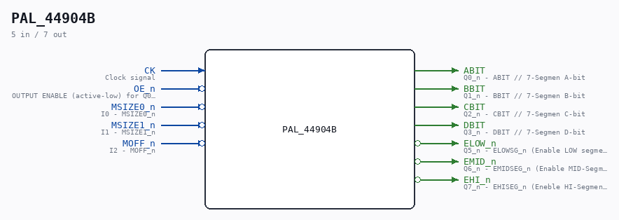
Schematic
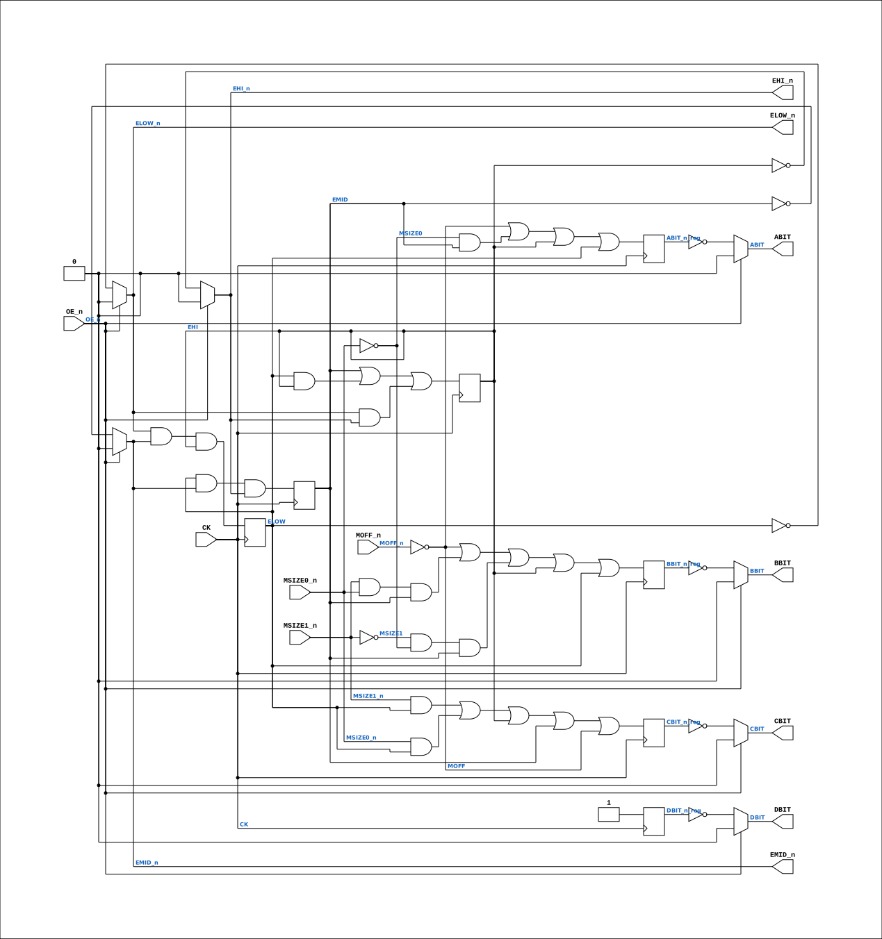
Drawn from the Verilog: the yosys netlist of the Simulation (Verilator) build, instance CORE.CPU_BOARD.MEM.ADEC.PAL_44904_UMSIZE. Sub-modules are boxes (click the picture to open it full size; there every sub-module box links to its page, and every wire shows its Verilog name).
Description
ND120 PALASM CODE CONVERTED TO VERILOG Component PAL 44904B Last reviewed: 2-FEB-2025 Ronny Hansen
Ports
| Direction | Width | Name | Description |
|---|---|---|---|
| input | 1 |
CK |
Clock signal |
| input | 1 |
OE_n (active low) |
OUTPUT ENABLE (active-low) for Q0-Q5 |
| input | 1 |
MSIZE0_n (active low) |
I0 - MSIZE0_n |
| input | 1 |
MSIZE1_n (active low) |
I1 - MSIZE1_n |
| input | 1 |
MOFF_n (active low) |
I2 - MOFF_n |
| output | 1 |
ABIT |
Q0_n - ABIT // 7-Segmen A-bit |
| output | 1 |
BBIT |
Q1_n - BBIT // 7-Segmen B-bit |
| output | 1 |
CBIT |
Q2_n - CBIT // 7-Segmen C-bit |
| output | 1 |
DBIT |
Q3_n - DBIT // 7-Segmen D-bit |
| output | 1 |
ELOW_n (active low) |
Q5_n - ELOWSG_n (Enable LOW segment) |
| output | 1 |
EMID_n (active low) |
Q6_n - EMIDSEG_n (Enable MID-Segment) |
| output | 1 |
EHI_n (active low) |
Q7_n - EHISEG_n (Eneble HI-Segment) |
Verilog source
Verilog/PAL/PAL_44904B.v on GitHub.
Show the Verilog of PAL_44904B (128 lines)
/**********************************************************************************************************
** ND120 PALASM CODE CONVERTED TO VERILOG                                                                **
**                                                                                                       **
** Component PAL 44904B                                                                                  **
**                                                                                                       **
** Last reviewed: 2-FEB-2025                                                                             **
** Ronny Hansen                                                                                          **
***********************************************************************************************************/


// PAL16R8
// CJTC 180587
// 44904B,7G,SIZEIND

//  RAM SIZE INDICATOR
//  Sheet 45 of 3202D

// PAL16R8 FAMILY
// PAL16R8 has 8 flip-flips, 8 inputs and 8 outputs (negated from flip-flops with 3-state support)

// https://rocelec.widen.net/view/pdf/c6dwcslffz/VANTS00080-1.pdf


// PCB 3202D sheet 45:
//
// PAL input signal PD4 is connected to PAL OE_n pin
//     output signal Q from CHIP 2D is connected to PAL CK pin (RLRQ signal)


module PAL_44904B (
    input CK,   //! Clock signal
    input OE_n, //! OUTPUT ENABLE (active-low) for Q0-Q5

    input MSIZE0_n,  //! I0 - MSIZE0_n
    input MSIZE1_n,  //! I1 - MSIZE1_n
    input MOFF_n,    //! I2 - MOFF_n
    //input i3,      //! I3 - (n.c.)
    //input i4,      //! I4 - (n.c.)
    //input i5,      //! I5 - (n.c.)
    //input i6,      //! I6 - (n.c.)
    //input i7,      //! I7 - (n.c.)

    output ABIT,    //! Q0_n - ABIT // 7-Segmen A-bit
    output BBIT,    //! Q1_n - BBIT // 7-Segmen B-bit
    output CBIT,    //! Q2_n - CBIT // 7-Segmen C-bit
    output DBIT,    //! Q3_n - DBIT // 7-Segmen D-bit
    //output Q4_n,  //! Q4_n - (n.c.)
    output ELOW_n,  //! Q5_n - ELOWSG_n (Enable LOW segment)
    output EMID_n,  //! Q6_n - EMIDSEG_n (Enable MID-Segment)
    output EHI_n    //! Q7_n - EHISEG_n (Eneble HI-Segment)

    //,output wire [3:0]  Q  // Enable to Debug to watch the value of Q change
);

  // negated input signals (not used signals are commented out)
  wire MSIZE0 = ~MSIZE0_n;
  wire MSIZE1 = ~MSIZE1_n;
  wire MOFF = ~MOFF_n;


  // Internal registers (for state-holding variables)
  reg EHI_reg, EMID_reg, ELOW_reg;
  reg ABIT_n_reg, BBIT_n_reg, CBIT_n_reg, DBIT_n_reg;

  // Internal wires
  wire EHI = EHI_reg;
  wire EMID = EMID_reg;
  wire ELOW = ELOW_reg;


  //**** Sequential logic triggered on the rising edge of CLK ****
  always @(posedge CK) begin


    // MEMORY SIZE INDICATOR FOR 0, 2, 4 OR 6 MB MEMORY ARRAYS

    EHI_reg    <= EMID | (ELOW & EHI) | (ELOW_n & EHI_n);  // Enable digit 3


    EMID_reg   <= ELOW & EMID_n & EHI_n;  // Enable digit 2

    ELOW_reg   <= ELOW_n & EMID_n & EHI;  // Enable digit 1

    ABIT_n_reg <= MOFF | (MSIZE0 & EMID) | EHI | ELOW;

    BBIT_n_reg <= MOFF | (MSIZE1_n & MSIZE0_n & EMID) | (MSIZE1 & MSIZE0 & EMID) | EHI | ELOW;

    CBIT_n_reg <= (MSIZE1_n & ELOW) | (MSIZE0_n & ELOW) | EHI | EMID | MOFF;

    DBIT_n_reg <= 1'b1;  // VCC, always high


  end

  // Tri-state control for Q outputs
  // Assigning outputs with three-state logic controlled by OE_n

  assign ABIT   = OE_n ? 1'b0 : ~ABIT_n_reg;  // Q0_n
  assign BBIT   = OE_n ? 1'b0 : ~BBIT_n_reg;  // Q1_n
  assign CBIT   = OE_n ? 1'b0 : ~CBIT_n_reg;  // Q2_n
  assign DBIT   = OE_n ? 1'b0 : ~DBIT_n_reg;  // Q3_n
                                              // Q4_n
  assign EHI_n  = OE_n ? 1'b0 : ~EHI_reg;  // Q5_n
  assign EMID_n = OE_n ? 1'b0 : ~EMID_reg;  // Q6_n
  assign ELOW_n = OE_n ? 1'b0 : ~ELOW_reg;  // Q7_n


endmodule

/*

DESCRIPTION

                MEMORY SIZE     S1  S0
                -----------     --  --
                    2MB          F   F
                    4MB          F   T
                    6MB          T   F
                    1MB          T   T


DIGIT ENABLE BITS : ELOW --> EMID --> EHI

; 170687 CJTC/JLB: ADDED 1MB INDICATION.
*/