MEM_43
Source: Verilog/CPU-BOARD-3202/circuit/MEM_43.v
Where it sits (Simulation): ND120_TOP > ND120_CORE > ND3202D > MEM_43
- instance path: CORE.CPU_BOARD.MEM
Used in: ND3202D (all tops)
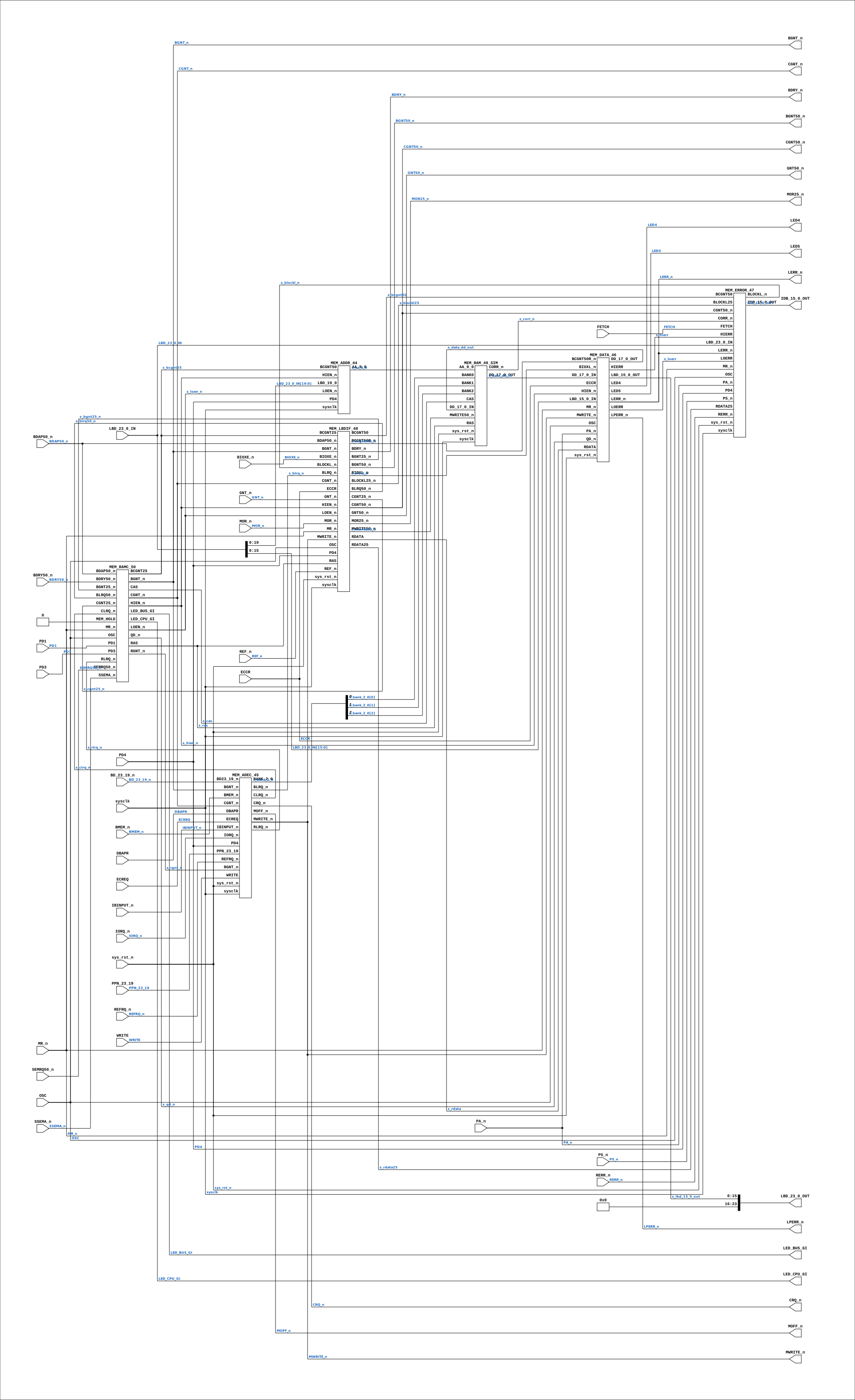
Contains: MEM_ADDR_44, MEM_ADEC_45, MEM_DATA_46, MEM_ERROR_47, MEM_LBDIF_48, MEM_RAM_49_BLOCKRAM (only on Basys3, Cmod), MEM_RAM_49_DDR2 (only on Nexys, MEGA65 R3), MEM_RAM_49_SDRAM (only on Tang, MiSTer, MEGA65 R6, QMTECH), MEM_RAM_49_SIM (only on Simulation), MEM_RAMC_50
Module hierarchy - All modules
Schematic
Drawn from the Verilog: the yosys netlist of the Simulation (Verilator) build, instance CORE.CPU_BOARD.MEM. Sub-modules are boxes (click the picture to open it full size; there every sub-module box links to its page, and every wire shows its Verilog name).
Description
ND120 CPU, MM&M MEM MEMORY TOP LEVEL SHEET 43 of 50 Last reviewed: 22-MAR-2025 Ronny Hansen
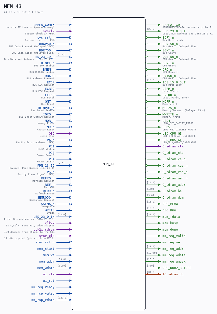
Ports
| Direction | Width | Name | Description |
|---|---|---|---|
| input | 1 |
ERRFA_CONTX |
console TX line in (probe arming) |
| output | 1 |
ERRFA_TXD |
SINTRAN ERRFATAL evidence probe TX (MEM_RAM_49_BLOCKRAM) |
| input | 1 |
sysclk |
System clock in FPGA |
| input | 1 |
sys_rst_n (active low) |
System reset in FPGA |
| input | 1 |
BDAP50_n (active low) |
BUS DAta Present (Delayed 50ns) |
| input | 1 |
BDRY50_n (active low) |
BUS Data ReadY (Delayed 50ns) |
| input | [4:0] |
BD_23_19_n (active low) |
Bus Data and Address (bits 23:19 negated) |
| input | 1 |
BIOXE_n (active low) |
BUS IOX Enable |
| input | 1 |
BMEM_n (active low) |
BUS MEMORY Enable |
| input | 1 |
DBAPR |
BUS Address Present |
| input | 1 |
ECCR |
BUS ECC Request |
| input | 1 |
ECREQ |
BUS ECC Request |
| input | 1 |
FETCH |
Bus Fetch |
| input | 1 |
GNT_n (active low) |
Bus Grant |
| input | 1 |
IBINPUT_n (active low) |
Bus Input Enable |
| input | 1 |
IORQ_n (active low) |
Bus Input/Output Request |
| input | 1 |
MOR_n (active low) |
Memory Error |
| input | 1 |
MR_n (active low) |
Master Reset |
| input | 1 |
OSC |
Oscillator |
| input | 1 |
PA_n (active low) |
Parity Error Address (PEA) |
| input | 1 |
PD1 |
Power Down 1 |
| input | 1 |
PD3 |
Power Down 3 |
| input | 1 |
PD4 |
Power Down 4 |
| input | [4:0] |
PPN_23_19 |
Physical Page Number Bits 23:19 |
| input | 1 |
PS_n (active low) |
Parity Error Signal (PES) |
| input | 1 |
REFRQ_n (active low) |
Refresh Request |
| input | 1 |
REF_n (active low) |
Refresh |
| input | 1 |
RERR_n (active low) |
Refresh Error |
| input | 1 |
SEMRQ50_n (active low) |
Semaphore Request |
| input | 1 |
SSEMA_n (active low) |
Semaphore |
| input | 1 |
WRITE |
Write |
| input | [23:0] |
LBD_23_0_IN |
Local Bus Address and Data 23:0 (IN) - Address and Data for RAM |
| output | [23:0] |
LBD_23_0_OUT |
Local Bus Address and Data 23:0 (OUT) - Data from from RAM (15:0) |
| output | 1 |
BDRY_n (active low) |
Bus Data Ready |
| output | 1 |
BGNT50_n (active low) |
Bus Grant (Delayed 50ns) |
| output | 1 |
BGNT_n (active low) |
Bus Grant |
| output | 1 |
CGNT50_n (active low) |
CPU Grant (Delayed 50ns) |
| output | 1 |
CGNT_n (active low) |
CPU Grant |
| output | 1 |
CRQ_n (active low) |
CPU Request |
| output | 1 |
GNT50_n (active low) |
CPU Grant (Delayed 50ns) |
| output | [15:0] |
IDB_15_0_OUT |
Bus Data 15:0 |
| output | 1 |
LERR_n (active low) |
Local Error |
| output | 1 |
LPERR_n (active low) |
Local Parity Error |
| output | 1 |
MOFF_n (active low) |
Memory Off |
| output | 1 |
MOR25_n (active low) |
Memory Request (Delayed 25ns) |
| output | 1 |
MWRITE_n (active low) |
Memory Write |
| output | 1 |
LED4 |
LED4_RED_PARITY_ERROR |
| output | 1 |
LED5 |
LED5_RED_DISABLE_PARITY |
| output | 1 |
LED_CPU_GI |
LED_CPU_GRANT_INDICATOR |
| output | 1 |
LED_BUS_GI |
LED_BUS_GRANT_INDICATOR |
| input | 1 |
clk2x |
2x sysclk, same PLL, edge-aligned |
| input | 1 |
clk2x_sdram |
180 degrees from clk2x, to the SDRAM chip |
| output | 1 |
O_sdram_clk |
|
| output | 1 |
O_sdram_cke |
|
| output | 1 |
O_sdram_cs_n (active low) |
|
| output | 1 |
O_sdram_cas_n (active low) |
|
| output | 1 |
O_sdram_ras_n (active low) |
|
| output | 1 |
O_sdram_wen_n (active low) |
|
| inout | [31:0] |
IO_sdram_dq |
|
| output | [10:0] |
O_sdram_addr |
|
| output | [1:0] |
O_sdram_ba |
|
| output | [3:0] |
O_sdram_dqm |
|
| output | [15:0] |
DBG_MEMW |
|
| output | [15:0] |
DBG_PGW |
|
| input | 1 |
stor_clk |
27 MHz crystal (pin 4) (from ND120_TANG20K_TOP.sys_clk) |
| input | 1 |
stor_rst_n (active low) |
|
| input | 1 |
mem_start |
|
| input | 1 |
mem_we |
|
| input | [19:0] |
mem_addr |
|
| input | [31:0] |
mem_wdata |
|
| output | [31:0] |
mem_rdata |
|
| output | 1 |
mem_busy |
|
| output | 1 |
mem_done |
|
| input | 1 |
ui_clk |
|
| input | 1 |
ui_rst |
|
| output | 1 |
mm_req_valid |
|
| output | 1 |
mm_req_we |
|
| output | [26:0] |
mm_req_addr |
|
| output | [127:0] |
mm_req_wdata |
|
| output | [15:0] |
mm_req_wmask |
|
| input | 1 |
mm_req_ready |
|
| input | 1 |
mm_rsp_valid |
|
| input | [127:0] |
mm_rsp_rdata |
|
| output | [7:0] |
DBG_DDR2_BRIDGE |
Verilog source
Verilog/CPU-BOARD-3202/circuit/MEM_43.v on GitHub.
Show the Verilog of MEM_43 (716 lines)
/**************************************************************************
** ND120 CPU, MM&M **
** MEM **
** MEMORY TOP LEVEL **
** SHEET 43 of 50 **
** **
** Last reviewed: 22-MAR-2025 **
** Ronny Hansen **
***************************************************************************/
module MEM_43 (
`ifdef ND120_ERRFA_PROBE
input ERRFA_CONTX, // console TX line in (probe arming)
output ERRFA_TXD, // SINTRAN ERRFATAL evidence probe TX (MEM_RAM_49_BLOCKRAM)
`endif
// Input signals
input sysclk, // System clock in FPGA
input sys_rst_n, // System reset in FPGA
input BDAP50_n, //! BUS DAta Present (Delayed 50ns)
input BDRY50_n, //! BUS Data ReadY (Delayed 50ns)
input [4:0] BD_23_19_n, //! Bus Data and Address (bits 23:19 negated)
input BIOXE_n, //! BUS IOX Enable
input BMEM_n, //! BUS MEMORY Enable
input DBAPR, //! BUS Address Present
input ECCR, //! BUS ECC Request
input ECREQ, //! BUS ECC Request
input FETCH, //! Bus Fetch
input GNT_n, //! Bus Grant
input IBINPUT_n, //! Bus Input Enable
input IORQ_n, //! Bus Input/Output Request
input MOR_n, //! Memory Error
input MR_n, //! Master Reset
input OSC, //! Oscillator
input PA_n, //! Parity Error Address (PEA)
input PD1, //! Power Down 1
input PD3, //! Power Down 3
input PD4, //! Power Down 4
input [4:0] PPN_23_19, //! Physical Page Number Bits 23:19
input PS_n, //! Parity Error Signal (PES)
input REFRQ_n, //! Refresh Request
input REF_n, //! Refresh
input RERR_n, //! Refresh Error
input SEMRQ50_n, //! Semaphore Request
input SSEMA_n, //! Semaphore
input WRITE, //! Write
input [23:0] LBD_23_0_IN, //! Local Bus Address and Data 23:0 (IN) - Address and Data for RAM
output [23:0] LBD_23_0_OUT, //! Local Bus Address and Data 23:0 (OUT) - Data from from RAM (15:0)
// Output signals
output BDRY_n, //! Bus Data Ready
output BGNT50_n, //! Bus Grant (Delayed 50ns)
output BGNT_n, //! Bus Grant
output CGNT50_n, //! CPU Grant (Delayed 50ns)
output CGNT_n, //! CPU Grant
output CRQ_n, //! CPU Request
output GNT50_n, //! CPU Grant (Delayed 50ns)
output [15:0] IDB_15_0_OUT, //! Bus Data 15:0
output LERR_n, //! Local Error
output LPERR_n, //! Local Parity Error
output MOFF_n, //! Memory Off
output MOR25_n, //! Memory Request (Delayed 25ns)
output MWRITE_n, //! Memory Write
output LED4, //! LED4_RED_PARITY_ERROR
output LED5, //! LED5_RED_DISABLE_PARITY
output LED_CPU_GI, //! LED_CPU_GRANT_INDICATOR
output LED_BUS_GI // LED_BUS_GRANT_INDICATOR
`ifdef MAIN_RAM_SDRAM
// SDRAM main-memory backend (Tang Nano 20K): the sheet-49 RAM is replaced
// by MEM_RAM_49_SDRAM, which needs a 2x clock pair and the SDRAM device
// pins threaded to the top level. Absent in Verilator/Basys3 builds.
,
input clk2x, //! 2x sysclk, same PLL, edge-aligned
input clk2x_sdram, //! 180 degrees from clk2x, to the SDRAM chip
output O_sdram_clk,
output O_sdram_cke,
output O_sdram_cs_n,
output O_sdram_cas_n,
output O_sdram_ras_n,
output O_sdram_wen_n,
inout [31:0] IO_sdram_dq,
output [10:0] O_sdram_addr,
output [ 1:0] O_sdram_ba,
output [ 3:0] O_sdram_dqm,
// Write-path debug: raw signal bus for the on-chip capture (see top)
output [15:0] DBG_MEMW,
//! SDRAM-bridge page-write watch (24-AUG zero-page campaign): every access
//! to physical rows 1016..1023 in both banks, taken AT THE BRIDGE.
output [15:0] DBG_PGW
`ifdef ND_STORAGE_PORT
// nd_storage device port, passed straight down to MEM_RAM_49_SDRAM (which
// forces the leading address 1, so device traffic physically cannot reach
// the CPU's half of the chip). stor_clk is its OWN domain - the backend
// toggle-CDCs it into clk2x. See MEM_RAM_49_SDRAM.v section 5.2.
,
input wire stor_clk, //! 27 MHz crystal (pin 4) (from ND120_TANG20K_TOP.sys_clk)
input wire stor_rst_n,
input wire mem_start,
input wire mem_we,
input wire [19:0] mem_addr,
input wire [31:0] mem_wdata,
output wire [31:0] mem_rdata,
output wire mem_busy,
output wire mem_done
`endif
`endif
`ifdef MAIN_RAM_DDR2
// DDR2 main-memory backend (Nexys 4 DDR): the sheet-49 RAM is replaced by
// MEM_RAM_49_DDR2 (BRAM cache in front of the MIG, reached through
// nd_ddr2_arb at the board top). The ui_clk-domain client port is
// threaded to the top level. MEM_HOLD never leaves this sheet - it
// freezes the two control PALs inside MEM_RAMC_50 on a cache miss.
,
input wire ui_clk,
input wire ui_rst,
output wire mm_req_valid,
output wire mm_req_we,
output wire [ 26:0] mm_req_addr,
output wire [127:0] mm_req_wdata,
output wire [ 15:0] mm_req_wmask,
input wire mm_req_ready,
input wire mm_rsp_valid,
input wire [127:0] mm_rsp_rdata,
output wire [ 7:0] DBG_DDR2_BRIDGE
`endif
);
/*******************************************************************************
** The wires are defined here **
*******************************************************************************/
wire [ 2:0] s_bank_2_0;
wire [ 4:0] s_bus_bd;
`ifdef MAIN_RAM_DDR2
wire s_mem_hold; // cache-miss cycle stretch from MEM_RAM_49_DDR2
`else
wire s_mem_hold = 1'b0;
`endif
wire [ 4:0] s_bus_ppn;
wire [ 9:0] s_aa_9_0;
wire [15:0] s_idb_15_0_out;
wire [17:0] s_data_dd_in;
wire [17:0] s_data_dd_out;
wire [17:0] s_ram_dd_17_0_in; // INPUT TO MEM_DATA
wire [17:0] s_ram_dd_17_0_out; // OUTPUT FROM MEM_DATA
wire [23:0] s_lbd_23_0_in; // RAM DATA 16 bits and ADDRESS 24 bits
wire [15:0] s_lbd_15_0_out; // RAM DATA 16 bits
wire s_bcgnt50;
wire s_bcgnt50r_n;
wire s_bdap50_n;
wire s_bdry;
wire s_bdry50_n;
wire s_bgnt_n;
wire s_bgnt25_n;
wire s_bcgnt25;
wire s_bgnt50_n;
wire s_bioxe_n;
wire s_bioxl_n;
wire s_blockl_n;
wire s_blockl25;
wire s_blrq_n;
wire s_blrq50_n;
wire s_bmem_n;
wire s_cas;
wire s_cgnt_n;
wire s_cgnt25_n;
wire s_cgnt50_n;
wire s_clrq_n;
wire s_corr_n;
wire s_crq_n;
wire s_dbapr;
wire s_eccr;
wire s_ecreq;
wire s_fetch;
wire s_gnt_n;
wire s_gnt50_n;
wire s_hien_n;
wire s_hierr;
wire s_ibinput_n;
wire s_iorq_n;
wire s_lerr_n;
wire s_loen_n;
wire s_loerr;
wire s_lperr_n;
wire s_moff_n;
wire s_mor_n;
wire s_mor25_n;
wire s_mr_n;
wire s_mwrite_n;
wire s_mwrite50_n;
wire s_osc;
wire s_pa_n;
wire s_pd1;
wire s_pd3;
wire s_pd4;
wire s_ps_n;
wire s_qd_n;
wire s_ras;
wire s_rdata;
wire s_rdata25;
wire s_ref_n;
wire s_refrq_n;
wire s_rerr_n;
wire s_rgnt_n;
wire s_rlrq_n;
wire s_semreq50_n;
wire s_ssema_n;
wire s_write;
/*******************************************************************************
** Here all input connections are defined **
*******************************************************************************/
assign s_bus_bd[4:0] = BD_23_19_n;
assign s_bus_ppn[4:0] = PPN_23_19;
assign s_lbd_23_0_in[23:0] = LBD_23_0_IN[23:0];
assign s_ibinput_n = IBINPUT_n;
assign s_pd3 = PD3;
assign s_dbapr = DBAPR;
assign s_ref_n = REF_n;
assign s_pa_n = PA_n;
assign s_iorq_n = IORQ_n;
assign s_ecreq = ECREQ;
assign s_pd1 = PD1;
assign s_semreq50_n = SEMRQ50_n;
assign s_gnt_n = GNT_n;
assign s_ssema_n = SSEMA_n;
assign s_ps_n = PS_n;
assign s_bmem_n = BMEM_n;
assign s_bioxe_n = BIOXE_n;
assign s_bdry50_n = BDRY50_n;
assign s_bdap50_n = BDAP50_n;
assign s_eccr = ECCR;
assign s_mor_n = MOR_n;
assign s_mr_n = MR_n;
assign s_refrq_n = REFRQ_n;
assign s_rerr_n = RERR_n;
assign s_osc = OSC;
assign s_fetch = FETCH;
assign s_pd4 = PD4;
assign s_write = WRITE;
/*******************************************************************************
** Here all output connections are defined **
*******************************************************************************/
assign BDRY_n = s_bdry;
assign BGNT50_n = s_bgnt50_n;
assign BGNT_n = s_bgnt_n;
assign CGNT50_n = s_cgnt50_n;
assign CGNT_n = s_cgnt_n;
assign CRQ_n = s_crq_n;
assign GNT50_n = s_gnt50_n;
assign IDB_15_0_OUT = s_idb_15_0_out[15:0];
assign LERR_n = s_lerr_n;
// The 74LS112 local-parity-error flip-flop (8J, sheet 46 region F6) was
// computed and then thrown away by the `| 1`, so LPERR~ could never go
// active. Restored - see the note in MEM_DATA_46.v about why memory
// classifies as Mpm 5 rather than Local when nothing can report an error.
assign LPERR_n = s_lperr_n;
assign MOFF_n = s_moff_n;
assign MOR25_n = s_mor25_n;
assign MWRITE_n = s_mwrite_n;
assign LBD_23_0_OUT = {8'b00000000, s_lbd_15_0_out};
/*******************************************************************************
** Here all internal busses are connected **
*******************************************************************************/
assign s_data_dd_in = s_ram_dd_17_0_out;
assign s_ram_dd_17_0_in = s_data_dd_out;
/*******************************************************************************
** Here all sub-circuits are defined **
*******************************************************************************/
/*
* Memory address decoder for the ND120 CPU system.
* Decodes the address bus and generates the address for the memory module.
* Also handles the memory control signals and error handling.
*/
MEM_ADEC_45 ADEC
(
.sysclk(sysclk),
.sys_rst_n(sys_rst_n),
// Inputs
.BGNT_n(s_bgnt_n),
.BMEM_n(s_bmem_n),
.CGNT_n(s_cgnt_n),
.DBAPR(s_dbapr),
.ECREQ(s_ecreq),
.IBINPUT_n(s_ibinput_n),
.IORQ_n(s_iorq_n),
.PD4(s_pd4),
.REFRQ_n(s_refrq_n),
.RGNT_n(s_rgnt_n),
.WRITE(s_write),
.BD23_19_n(s_bus_bd[4:0]),
.PPN_23_19(s_bus_ppn[4:0]),
// Outputs
.BANK_2_0(s_bank_2_0[2:0]),
.BLRQ_n(s_blrq_n),
.CLRQ_n(s_clrq_n),
.CRQ_n(s_crq_n),
.MOFF_n(s_moff_n),
.MWRITE_n(s_mwrite_n),
.RLRQ_n(s_rlrq_n)
);
/*
* Memory local bus interface for the ND120 CPU system.
* Handles the local bus interface and memory control signals.
*/
MEM_LBDIF_48 LBDIF (
.sysclk(sysclk),
// Input signals
.BDAP50_n(s_bdap50_n),
.BGNT25_n(s_bgnt25_n),
.BGNT50_n(s_bgnt50_n),
.BGNT_n(s_bgnt_n),
.BIOXE_n(s_bioxe_n),
.BLRQ50_n(s_blrq50_n),
.BLRQ_n(s_blrq_n),
.CGNT25_n(s_cgnt25_n),
.CGNT50_n(s_cgnt50_n),
.CGNT_n(s_cgnt_n),
.ECCR(s_eccr),
.GNT50_n(s_gnt50_n),
.GNT_n(s_gnt_n),
.MOR_n(s_mor_n),
.MR_n(s_mr_n),
.MWRITE_n(s_mwrite_n),
.OSC(s_osc),
.sys_rst_n(sys_rst_n),
.PD4(s_pd4),
.REF_n(s_ref_n),
// Output signals
.BCGNT25(s_bcgnt25),
.BCGNT50(s_bcgnt50),
.BCGNT50R_n(s_bcgnt50r_n),
.BDRY_n(s_bdry),
.BIOXL_n(s_bioxl_n),
.BLOCKL25_n(s_blockl25),
.BLOCKL_n(s_blockl_n),
.HIEN_n(s_hien_n),
.LOEN_n(s_loen_n),
.MOR25_n(s_mor25_n),
.MWRITE50_n(s_mwrite50_n),
.RAS(s_ras),
.RDATA(s_rdata),
.RDATA25(s_rdata25)
);
/*
* Memory data handling module for the ND120 CPU system.
* Handles data transfer between the memory and the CPU.
*/
MEM_DATA_46 DATA (
.OSC(s_osc), // Clock (added for FPGA synthesis)
.sys_rst_n(sys_rst_n), // System reset (for FPGA synthesis)
// Input signals
.BCGNT50R_n(s_bcgnt50r_n),
.BIOXL_n(s_bioxl_n),
.DD_17_0_IN(s_data_dd_in[17:0]),
.ECCR(s_eccr),
.HIEN_n(s_hien_n),
.LBD_15_0_IN(s_lbd_23_0_in[15:0]),
.MR_n(s_mr_n),
.MWRITE_n(s_mwrite_n),
.PA_n(s_pa_n),
.QD_n(s_qd_n),
.RDATA(s_rdata),
// Output signals
.DD_17_0_OUT(s_data_dd_out[17:0]),
.HIERR(s_hierr),
.LBD_15_0_OUT(s_lbd_15_0_out[15:0]),
.LED4(LED4),
.LED5(LED5),
.LERR_n(s_lerr_n),
.LOERR(s_loerr),
.LPERR_n(s_lperr_n)
);
/*
* Memory error handling module for the ND120 CPU system.
* Handles memory error detection and reporting.
*/
MEM_ERROR_47 ERROR (
// Clock and reset (added for FPGA synthesis)
.sysclk(sysclk),
.OSC(s_osc),
.sys_rst_n(sys_rst_n),
// Input signals
.BCGNT50(s_bcgnt50),
.BLOCKL25(s_blockl25),
.BLOCKL_n(s_blockl_n),
.CGNT50_n(s_cgnt50_n),
.CORR_n(s_corr_n),
.FETCH(s_fetch),
.LBD_23_0_IN(s_lbd_23_0_in[23:0]),
.MR_n(s_mr_n),
.PA_n(s_pa_n),
.PD4(s_pd4),
.PS_n(s_ps_n),
.RDATA25(s_rdata25),
.RERR_n(s_rerr_n),
// Output signals
.HIERR(s_hierr),
.IDB_15_0_OUT(s_idb_15_0_out[15:0]),
.LERR_n(s_lerr_n),
.LOERR(s_loerr)
);
/*
* Memory RAM control module for the ND120 CPU system.
* Handles memory control signals and error handling.
*/
MEM_RAMC_50 RAMC (
// Input signals
.BDAP50_n(s_bdap50_n),
.BDRY50_n(s_bdry50_n),
.BCGNT25(s_bcgnt25),
.BGNT25_n(s_bgnt25_n),
.BGNT_n(s_bgnt_n),
.BLRQ50_n(s_blrq50_n),
.CAS(s_cas),
.CGNT25_n(s_cgnt25_n),
.CGNT_n(s_cgnt_n),
.CLRQ_n(s_clrq_n),
.HIEN_n(s_hien_n),
.LOEN_n(s_loen_n),
.MR_n(s_mr_n),
.OSC(s_osc),
.PD1(s_pd1),
.PD3(s_pd3),
.QD_n(s_qd_n),
.RAS(s_ras),
.RGNT_n(s_rgnt_n),
.RLRQ_n(s_rlrq_n),
.SEMRQ50_n(s_semreq50_n),
.SSEMA_n(s_ssema_n),
.MEM_HOLD(s_mem_hold),
// Output signals
.LED_CPU_GI(LED_CPU_GI),
.LED_BUS_GI(LED_BUS_GI)
);
/*
* Memory address decoder for the ND120 CPU system.
* Decodes the address bus and generates the address for the memory module.
* Also handles the memory control signals and error handling.
*/
MEM_ADDR_44 ADDR (
.sysclk(sysclk),
// Input signals
.BCGNT50(s_bcgnt25), // Need to latch address earlier before it goes away. Thats why this is changed to BCGNT25 (Ronny 7.12.2024)
.HIEN_n(s_hien_n),
.LBD_19_0(s_lbd_23_0_in[19:0]),
.LOEN_n(s_loen_n),
.PD4(s_pd4),
// Output signals
.AA_9_0(s_aa_9_0[9:0])
);
/*
* Top level memory module for the ND120 CPU system.
* Handles memory operations and interfaces with the system bus.
* Provides memory access, control and error handling functionality.
*/
`ifdef MAIN_RAM_SDRAM
// Raw write-path signal bus for the top-level capture engine.
// v4: bridge-FSM focus (v3 proved AA row/col + BANK0 + write mode are all
// correct at the bridge inputs, so the break is inside the bridge or the
// SDRAM controller - watch commands issue and data_ready come back).
// Bits [7:6] are 0 here; ND3202D overlays wdec (trigger) and WRITE.
wire [7:0] s_dbg_bridge;
assign DBG_MEMW = {s_dbg_bridge[7:0], // [15:8] bridge: {bstate[2:0],
// wr, rd, data_ready, have_data, busy}
2'b00, // [7:6] (wdec, WRITE in ND3202D)
s_bank_2_0[0], // [5] BANK0
s_mwrite50_n, // [4]
s_dbapr, // [3]
s_ecreq, // [2]
s_cas, // [1]
s_ras}; // [0]
// Tang Nano 20K: sheet-49 RAM implemented on the embedded 8 MB SDRAM
// (fpga/tang-nano-20k/sdram-bridge/MEM_RAM_49_SDRAM.v; same interface,
// 2 banks = 4 MB, self-scheduled refresh - see docs/nd120-dram-memory.md)
MEM_RAM_49_SDRAM RAM (
.sysclk(sysclk),
.sys_rst_n(sys_rst_n),
// Input signals
.AA_9_0(s_aa_9_0[9:0]),
.BANK0(s_bank_2_0[0]),
.BANK1(s_bank_2_0[1]),
.BANK2(s_bank_2_0[2]),
.CAS(s_cas),
.CORR_n(s_corr_n),
.DD_17_0_IN(s_ram_dd_17_0_in[17:0]),
.MWRITE50_n(s_mwrite50_n),
.RAS(s_ras),
// Output signals
.DD_17_0_OUT(s_ram_dd_17_0_out[17:0]),
// SDRAM backend (threaded to the board top)
.clk2x(clk2x),
.clk2x_sdram(clk2x_sdram),
.O_sdram_clk(O_sdram_clk),
.O_sdram_cke(O_sdram_cke),
.O_sdram_cs_n(O_sdram_cs_n),
.O_sdram_cas_n(O_sdram_cas_n),
.O_sdram_ras_n(O_sdram_ras_n),
.O_sdram_wen_n(O_sdram_wen_n),
.IO_sdram_dq(IO_sdram_dq),
.DBG_BRIDGE(s_dbg_bridge),
.DBG_PGW(DBG_PGW),
.O_sdram_addr(O_sdram_addr),
.O_sdram_ba(O_sdram_ba),
.O_sdram_dqm(O_sdram_dqm)
`ifdef ND_STORAGE_PORT
,
.stor_clk (stor_clk),
.stor_rst_n(stor_rst_n),
.mem_start (mem_start),
.mem_we (mem_we),
.mem_addr (mem_addr),
.mem_wdata (mem_wdata),
.mem_rdata (mem_rdata),
.mem_busy (mem_busy),
.mem_done (mem_done)
`endif
);
`elsif MAIN_RAM_DDR2
// Nexys 4 DDR: sheet-49 RAM implemented as a BRAM cache in front of the
// 128 MiB DDR2 (fpga/nexys4ddr/ddr2/MEM_RAM_49_DDR2.v; same interface,
// BANK0+BANK2 = 4 MB like the Tang, BANK1 absent). A cache miss freezes
// the two control PALs (MEM_HOLD) until the line arrives - the CPU waits
// via CGNTCACT_n, DMA via BDRY_n; see the module header for the proof.
`ifndef ND120_DDR2_CACHE_BITS
`define ND120_DDR2_CACHE_BITS 14
`endif
MEM_RAM_49_DDR2 #(
.CACHE_IDX_BITS(`ND120_DDR2_CACHE_BITS)
) RAM (
.sysclk(sysclk),
.sys_rst_n(sys_rst_n),
.AA_9_0(s_aa_9_0[9:0]),
.BANK0(s_bank_2_0[0]),
.BANK1(s_bank_2_0[1]),
.BANK2(s_bank_2_0[2]),
.CAS(s_cas),
.RAS(s_ras),
.MWRITE50_n(s_mwrite50_n),
.DD_17_0_IN(s_ram_dd_17_0_in[17:0]),
.DD_17_0_OUT(s_ram_dd_17_0_out[17:0]),
.CORR_n(s_corr_n),
.MEM_HOLD(s_mem_hold),
// DDR2 client port, threaded to the board top (nd_ddr2_arb)
.ui_clk(ui_clk),
.ui_rst(ui_rst),
.mm_req_valid(mm_req_valid),
.mm_req_we(mm_req_we),
.mm_req_addr(mm_req_addr),
.mm_req_wdata(mm_req_wdata),
.mm_req_wmask(mm_req_wmask),
.mm_req_ready(mm_req_ready),
.mm_rsp_valid(mm_rsp_valid),
.mm_rsp_rdata(mm_rsp_rdata),
.DBG_BRIDGE(DBG_DDR2_BRIDGE)
);
`elsif MAIN_RAM_BLOCKRAM
// FPGA block-RAM backend: one clean synchronous BRAM instead of the six
// emulated SIP1M9 chips (MEM_RAM_49_BLOCKRAM.v). Default 3 banks x 4K words
// (Basys3 xc7a35t budget); boards with more BRAM override the words-per-bank
// exponent with ND120_BLOCKRAM_ADDR_BITS (Nexys 4 DDR sets 15 = 32K words
// per bank in fpga/nexys4ddr/build.tcl).
`ifndef ND120_BLOCKRAM_ADDR_BITS
`define ND120_BLOCKRAM_ADDR_BITS 12
`endif
// Bank slots the array is declared with: 4 (default, unchanged for every
// proven build) or 3 (MiSTer: only banks 0-2 exist, and the fourth slot
// is what kept a 64K-word bank from fitting the Cyclone V; a 32K-word bank
// wraps addresses >= 0o100000 and is the LIST-FILE-NAMES runaway of
// 24-AUG-2026 - Verilog/docs/nd120-facts.md).
`ifndef ND120_BLOCKRAM_BANK_SLOTS
`define ND120_BLOCKRAM_BANK_SLOTS 4
`endif
MEM_RAM_49_BLOCKRAM #(
.BANK_ADDR_BITS(`ND120_BLOCKRAM_ADDR_BITS),
.BANK_SLOTS (`ND120_BLOCKRAM_BANK_SLOTS)
) RAM (
`ifdef ND120_ERRFA_PROBE
.ERRFA_CONTX(ERRFA_CONTX),
.ERRFA_TXD(ERRFA_TXD),
`endif
.sysclk(sysclk),
.sys_rst_n(sys_rst_n),
.AA_9_0(s_aa_9_0[9:0]),
.BANK0(s_bank_2_0[0]),
.BANK1(s_bank_2_0[1]),
.BANK2(s_bank_2_0[2]),
.CAS(s_cas),
.CORR_n(s_corr_n),
.DD_17_0_IN(s_ram_dd_17_0_in[17:0]),
.MWRITE50_n(s_mwrite50_n),
.RAS(s_ras),
.DD_17_0_OUT(s_ram_dd_17_0_out[17:0])
);
`elsif VERILATOR_SIM
// Simulation backend: the zero-delay DRAM model on the shared sheet-49
// interface (MEM_RAM_49_SIM.v, 3 banks x 1M x 18 bits = 6 MB - onboard
// decode reaches a 4 MB window, fully backed). This is the RAM that the
// sim builds actually compile; the SIP1M9 `else` branch below is NOT
// used by the sim. The C++ harnesses preload/inspect programs directly
// through its b0_* arrays (e.g. runSim/Run120.cpp reads ...RAM__DOT__b0_lo).
//
// To model a small FPGA-size RAM in a Verilator build instead, define
// MAIN_RAM_BLOCKRAM (selects MEM_RAM_49_BLOCKRAM above). NOTE: FORCE_SMALL_RAM
// is unrelated - it is a RAM_SIZE guard inside the legacy MEM_RAM_49.v
// (SIP1M9) and has NO effect on this MEM_RAM_49_SIM module.
MEM_RAM_49_SIM RAM (
.sysclk(sysclk),
.sys_rst_n(sys_rst_n),
.AA_9_0(s_aa_9_0[9:0]),
.BANK0(s_bank_2_0[0]),
.BANK1(s_bank_2_0[1]),
.BANK2(s_bank_2_0[2]),
.CAS(s_cas),
.CORR_n(s_corr_n),
.DD_17_0_IN(s_ram_dd_17_0_in[17:0]),
.MWRITE50_n(s_mwrite50_n),
.RAS(s_ras),
.DD_17_0_OUT(s_ram_dd_17_0_out[17:0])
);
`elsif MAIN_RAM_SIP1M9
// ===========================================================================
// OPT-IN ONLY (3-AUG-2026): the original six-chip SIP1M9 sheet
// (MEM_RAM_49.v + Shared/support/SIP1M9.v), kept as a schematic-faithful
// reference of the real sheet-49 DRAM array. It is NO LONGER a fallback -
// a board reaches it only by defining MAIN_RAM_SIP1M9 deliberately.
//
// Why this changed: until today this was the `else branch, and its own
// comment claimed "NOT USED BY ANY CURRENT BUILD". That was WRONG. Basys3
// defined no MAIN_RAM_* at all - the real synthesis logs show only
// FPGA_FF_MODE, SKIP_WCS_LOAD, BOARD_CLK_FREQ and UART_BAUD_RATE - so it had
// been silently landing here, which is precisely what the old comment said
// must never happen. Basys3 now selects MAIN_RAM_BLOCKRAM explicitly in
// fpga/basys3/vivado_build.tcl, and a missing selection is a COMPILE ERROR
// (the `else below) instead of a silent choice.
//
// Backend map:
// * Verilator sim -> MEM_RAM_49_SIM (`elsif VERILATOR_SIM)
// * Tang Nano 20K -> MEM_RAM_49_SDRAM (`ifdef MAIN_RAM_SDRAM)
// * BRAM boards -> MEM_RAM_49_BLOCKRAM (`elsif MAIN_RAM_BLOCKRAM)
// * this reference -> MEM_RAM_49 (`elsif MAIN_RAM_SIP1M9)
// A new board either reuses one of those or adds its own
// MEM_RAM_49_<board>.v implementing the same sheet-49 interface (AA_9_0,
// BANK0/1/2, RAS, CAS, MWRITE50_n, DD_17_0_IN/OUT, CORR_n).
// ===========================================================================
MEM_RAM_49 RAM (
.sysclk(sysclk),
.sys_rst_n(sys_rst_n),
// Input signals
.AA_9_0(s_aa_9_0[9:0]),
.BANK0(s_bank_2_0[0]),
.BANK1(s_bank_2_0[1]),
.BANK2(s_bank_2_0[2]),
.CAS(s_cas),
.CORR_n(s_corr_n),
.DD_17_0_IN(s_ram_dd_17_0_in[17:0]),
.MWRITE50_n(s_mwrite50_n),
.RAS(s_ras),
// Output signals
.DD_17_0_OUT(s_ram_dd_17_0_out[17:0])
);
`else
// ===========================================================================
// NO MAIN MEMORY BACKEND SELECTED - this is a build-configuration error.
//
// Every build must choose one, explicitly:
// MAIN_RAM_SDRAM Tang Nano 20K (8 MB SDRAM via sdram-bridge)
// MAIN_RAM_BLOCKRAM BRAM boards (Basys3, Cmod A7, QMTech)
// VERILATOR_SIM Verilator harnesses (6 MB behavioural model)
// MAIN_RAM_SIP1M9 the six-chip sheet-49 reference (opt-in only)
//
// Instantiating a module that does not exist is the portable way to fail at
// ELABORATION in every tool we use (iverilog, Verilator, Vivado, Gowin) -
// there is no standard `error directive in Verilog-2001. The module name is
// the diagnostic; read it and go define one of the four above.
// ===========================================================================
ND120_ERROR_no_main_ram_backend_selected NO_RAM_BACKEND ();
`endif
endmodule