CPU_MMU_CSR_26
Source: Verilog/CPU-BOARD-3202/circuit/CPU_MMU_CSR_26.v
Where it sits (Simulation): ND120_TOP > ND120_CORE > ND3202D > CPU_15 > CPU_MMU_24 > CPU_MMU_CSR_26
- instance path: CORE.CPU_BOARD.CPU.MMU.CSR
Used in: CPU_MMU_24 (all tops)
Contains: no other modules.
Module hierarchy - All modules
Schematic
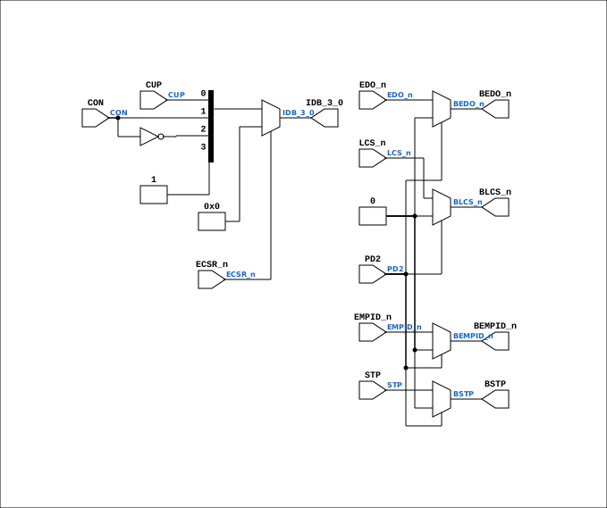
Drawn from the Verilog: the yosys netlist of the Simulation (Verilator) build, instance CORE.CPU_BOARD.CPU.MMU.CSR. Sub-modules are boxes (click the picture to open it full size; there every sub-module box links to its page, and every wire shows its Verilog name).
Description
ND120 CPU, MM&M CPU/MMU/CSR CACHE STATUS REGISER SHEET 26 of 50 Last reviewed: 29-JAN-2025 Ronny Hansen
Ports
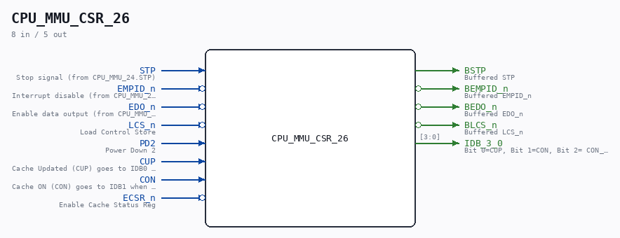
| Direction | Width | Name | Description |
|---|---|---|---|
| input | 1 |
STP |
Stop signal (from CPU_MMU_24.STP) |
| input | 1 |
EMPID_n (active low) |
Interrupt disable (from CPU_MMU_24.EMPID_n) |
| input | 1 |
EDO_n (active low) |
Enable data output (from CPU_MMU_24.EDO_n) |
| input | 1 |
LCS_n (active low) |
Load Control Store |
| input | 1 |
PD2 |
Power Down 2 |
| input | 1 |
CUP |
Cache Updated (CUP) goes to IDB0 when ECSR_n is low |
| input | 1 |
CON |
Cache ON (CON) goes to IDB1 when ECSR_n is low. CON_n goes to IDB2 |
| input | 1 |
ECSR_n (active low) |
Enable Cache Status Reg |
| output | 1 |
BSTP |
Buffered STP |
| output | 1 |
BEMPID_n (active low) |
Buffered EMPID_n |
| output | 1 |
BEDO_n (active low) |
Buffered EDO_n |
| output | 1 |
BLCS_n (active low) |
Buffered LCS_n |
| output | [3:0] |
IDB_3_0 |
Bit 0=CUP, Bit 1=CON, Bit 2= CON_n, Bit 3=1 (FIN-Cache Clear finished. Not currently enabled) |
Verilog source
Verilog/CPU-BOARD-3202/circuit/CPU_MMU_CSR_26.v on GitHub.
Show the Verilog of CPU_MMU_CSR_26 (46 lines)
/**************************************************************************
** ND120 CPU, MM&M                                                       **
** CPU/MMU/CSR                                                           **
** CACHE STATUS REGISER                                                  **
** SHEET 26 of 50                                                        **
**                                                                       **
** Last reviewed: 29-JAN-2025                                            **
** Ronny Hansen                                                          **
***************************************************************************/
module CPU_MMU_CSR_26 (
    input STP,    //! Stop signal (from CPU_MMU_24.STP)
    input EMPID_n,  //! Interrupt disable (from CPU_MMU_24.EMPID_n)
    input EDO_n,  //! Enable data output (from CPU_MMU_24.EDO_n)
    input LCS_n,  //! Load Control Store
    input PD2,    //! Power Down 2

    input CUP,    //! Cache Updated (CUP) goes to IDB0 when ECSR_n is low
    input CON,    //! Cache ON (CON) goes to IDB1 when ECSR_n is low. CON_n goes to IDB2
    input ECSR_n, //! Enable Cache Status Reg

    // IF PD2 goes active to 1, then all B-signals goes to high-impediance aka 0)
    output BSTP,      //! Buffered STP
    output BEMPID_n,  //! Buffered EMPID_n
    output BEDO_n,    //! Buffered EDO_n
    output BLCS_n,    //! Buffered LCS_n

    output [3:0] IDB_3_0  // Bit 0=CUP, Bit 1=CON, Bit 2= CON_n, Bit 3=1 (FIN-Cache Clear finished. Not currently enabled)
);


  // This code replaces one 74244 (CHIP 27H)
  // 74LS244 (NONE negated outputs)
  // Octal Buffers and Line Drivers With 3-State Outputs


  assign BSTP = PD2 ? 1'b0 : STP;
  assign BEMPID_n = PD2 ? 1'b0 : EMPID_n;
  assign BEDO_n = PD2 ? 1'b0 : EDO_n;
  assign BLCS_n = PD2 ? 1'b0 : LCS_n;

  wire [3:0] idb = {1'b1, ~CON, CON, CUP};

  assign IDB_3_0 = ECSR_n ? 4'b0 : idb;

endmodule