MEM_ADEC_45
Source: Verilog/CPU-BOARD-3202/circuit/MEM_ADEC_45.v
Where it sits (Simulation): ND120_TOP > ND120_CORE > ND3202D > MEM_43 > MEM_ADEC_45
- instance path: CORE.CPU_BOARD.MEM.ADEC
Used in: MEM_43 (all tops)
Contains: PAL_44445B_D, PAL_44446B_D, PAL_44904B
Module hierarchy - All modules
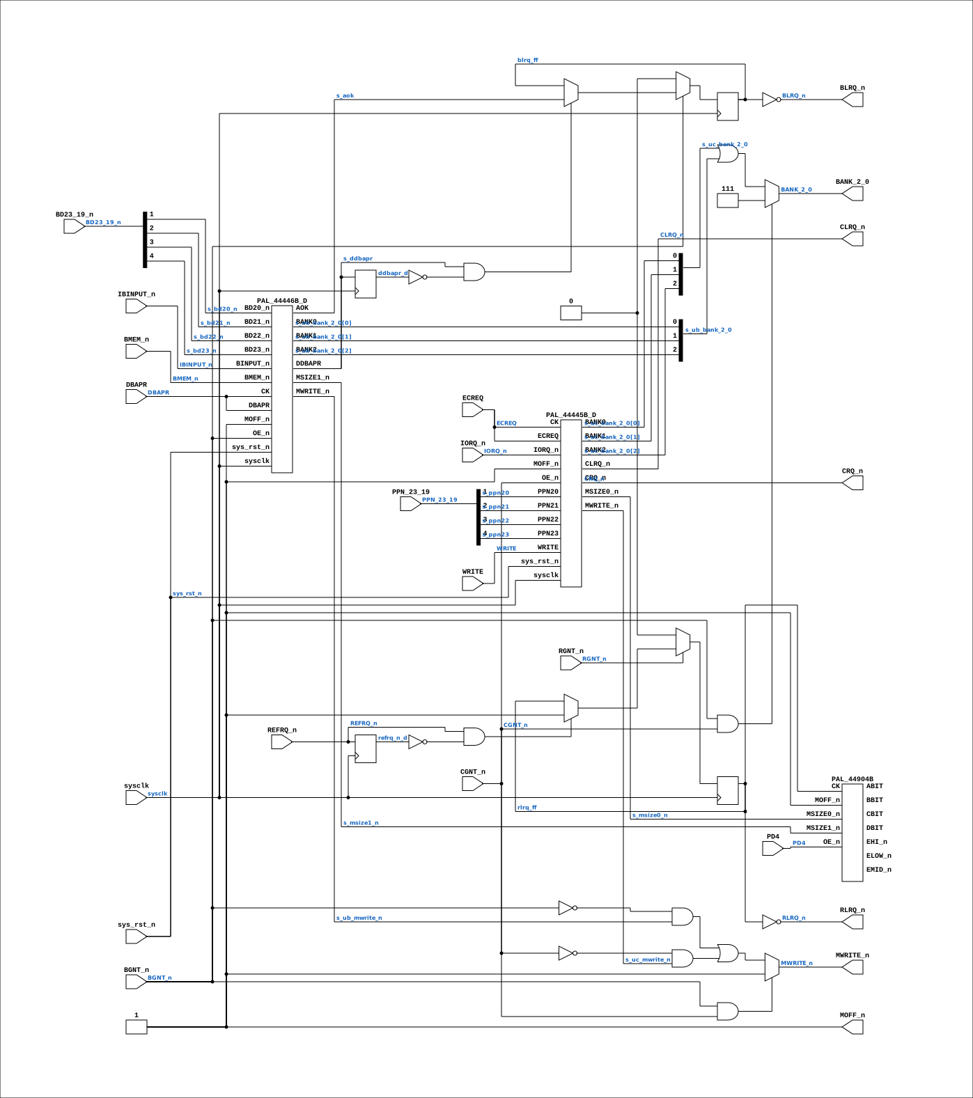
Schematic
Drawn from the Verilog: the yosys netlist of the Simulation (Verilator) build, instance CORE.CPU_BOARD.MEM.ADEC. Sub-modules are boxes (click the picture to open it full size; there every sub-module box links to its page, and every wire shows its Verilog name).
Description
ND120 CPU, MM&M MEM/ADEC ADDRESS DECODERS SHEET 45 of 50 Last reviewed: 22-MAR-2025 Ronny Hansen
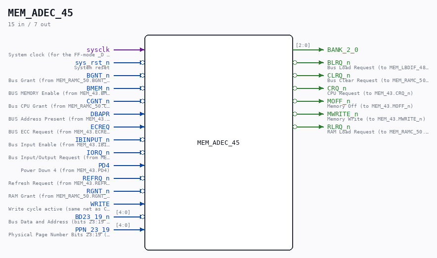
Ports
| Direction | Width | Name | Description |
|---|---|---|---|
| input | 1 |
sysclk |
System clock (for the FF-mode _D PAL mirrors) |
| input | 1 |
sys_rst_n (active low) |
System reset |
| input | 1 |
BGNT_n (active low) |
Bus Grant (from MEM_RAMC_50.BGNT_n) |
| input | 1 |
BMEM_n (active low) |
BUS MEMORY Enable (from MEM_43.BMEM_n) |
| input | 1 |
CGNT_n (active low) |
Bus CPU Grant (from MEM_RAMC_50.CGNT_n) |
| input | 1 |
DBAPR |
BUS Address Present (from MEM_43.DBAPR) |
| input | 1 |
ECREQ |
BUS ECC Request (from MEM_43.ECREQ) |
| input | 1 |
IBINPUT_n (active low) |
Bus Input Enable (from MEM_43.IBINPUT_n) |
| input | 1 |
IORQ_n (active low) |
Bus Input/Output Request (from MEM_43.IORQ_n) |
| input | 1 |
PD4 |
Power Down 4 (from MEM_43.PD4) |
| input | 1 |
REFRQ_n (active low) |
Refresh Request (from MEM_43.REFRQ_n) |
| input | 1 |
RGNT_n (active low) |
RAM Grant (from MEM_RAMC_50.RGNT_n) |
| input | 1 |
WRITE |
Write cycle active (same net as CPU_15.WRITE) |
| input | [4:0] |
BD23_19_n (active low) |
Bus Data and Address (bits 23:19 negated) (from MEM_43.BD_23_19_n) |
| input | [4:0] |
PPN_23_19 |
Physical Page Number Bits 23:19 (from MEM_43.PPN_23_19) |
| output | [2:0] |
BANK_2_0 |
|
| output | 1 |
BLRQ_n (active low) |
Bus Load Request (to MEM_LBDIF_48.BLRQ_n) |
| output | 1 |
CLRQ_n (active low) |
Bus Clear Request (to MEM_RAMC_50.CLRQ_n) |
| output | 1 |
CRQ_n (active low) |
CPU Request (to MEM_43.CRQ_n) |
| output | 1 |
MOFF_n (active low) |
Memory Off (to MEM_43.MOFF_n) |
| output | 1 |
MWRITE_n (active low) |
Memory Write (to MEM_43.MWRITE_n) |
| output | 1 |
RLRQ_n (active low) |
RAM Load Request (to MEM_RAMC_50.RLRQ_n) |
Verilog source
Verilog/CPU-BOARD-3202/circuit/MEM_ADEC_45.v on GitHub.
Show the Verilog of MEM_ADEC_45 (350 lines)
/**************************************************************************
** ND120 CPU, MM&M                                                       **
** MEM/ADEC                                                              **
** ADDRESS DECODERS                                                      **
** SHEET 45 of 50                                                        **
**                                                                       **
** Last reviewed: 22-MAR-2025                                            **
** Ronny Hansen                                                          **
***************************************************************************/


module MEM_ADEC_45 (
    input sysclk,     //! System clock (for the FF-mode _D PAL mirrors)
    input sys_rst_n,  //! System reset
    input BGNT_n,     //! Bus Grant (from MEM_RAMC_50.BGNT_n)
    input BMEM_n,     //! BUS MEMORY Enable (from MEM_43.BMEM_n)
    input CGNT_n,     //! Bus CPU Grant (from MEM_RAMC_50.CGNT_n)
    input DBAPR,      //! BUS Address Present (from MEM_43.DBAPR)
    input ECREQ,      //! BUS ECC Request (from MEM_43.ECREQ)
    input IBINPUT_n,  //! Bus Input Enable (from MEM_43.IBINPUT_n)
    input IORQ_n,     //! Bus Input/Output Request (from MEM_43.IORQ_n)
    input PD4,        //! Power Down 4 (from MEM_43.PD4)
    input REFRQ_n,    //! Refresh Request (from MEM_43.REFRQ_n)
    input RGNT_n,     //! RAM Grant (from MEM_RAMC_50.RGNT_n)
    input WRITE,      //! Write cycle active (same net as CPU_15.WRITE)

    input [4:0] BD23_19_n,  //! Bus Data and Address (bits 23:19 negated) (from MEM_43.BD_23_19_n)
    input [4:0] PPN_23_19,  //! Physical Page Number Bits 23:19 (from MEM_43.PPN_23_19)

    output [2:0] BANK_2_0,
    output BLRQ_n,    //! Bus Load Request (to MEM_LBDIF_48.BLRQ_n)
    output CLRQ_n,    //! Bus Clear Request (to MEM_RAMC_50.CLRQ_n)
    output CRQ_n,     //! CPU Request (to MEM_43.CRQ_n)
    output MOFF_n,    //! Memory Off (to MEM_43.MOFF_n)
    output MWRITE_n,  //! Memory Write (to MEM_43.MWRITE_n)
    output RLRQ_n     //! RAM Load Request (to MEM_RAMC_50.RLRQ_n)
);

  /*******************************************************************************
   ** The wires are defined here                                                 **
   *******************************************************************************/
  wire [2:0] s_bank_2_0_out;
  wire [2:0] s_uc_bank_2_0;
  wire [2:0] s_ub_bank_2_0;
  wire       s_abit;
  wire       s_aok;
  wire       s_bbit;
  wire       s_bd20_n;
  wire       s_bd21_n;
  wire       s_bd22_n;
  wire       s_bd23_n;
  wire       s_bgnt_n;
  wire       s_bgnt;
  wire       s_blrq_n_out;
  wire       s_bmem_n;
  wire       s_cbit;
  wire       s_cgnt_n;
  wire       s_clrq_n_out;
  wire       s_crq_n_out;
  wire       s_dbapr;
  wire       s_dbit;
  wire       s_ddbapr;
  wire       s_ecreq;
  wire       s_ehiseg_n;
  wire       s_elowseg_n;
  wire       s_emidseg_n;
  wire       s_gnd;
  wire       s_ibinput_n;
  wire       s_iorq_n;
  wire       s_moff_n;
  wire       s_msize0_n;
  wire       s_msize1_n;
  wire       s_mwrite_n_out;
  wire       s_uc_mwrite_n;
  wire       s_ub_mwrite_n;
  wire       s_pal_44904_clk;
  wire       s_pd4;
  wire       s_power;
  wire       s_ppn20;
  wire       s_ppn21;
  wire       s_ppn22;
  wire       s_ppn23;
  wire       s_refrq_n;
  wire       s_rgnt_n;
  wire       s_rgnt;
  wire       s_rlrq_n_out;
  wire       s_write;

  // Unused wires, this to keep LINTER happy and not complaining about bits not read
  (* keep = "true", DONT_TOUCH = "true" *) wire s_ppn19;
  (* keep = "true", DONT_TOUCH = "true" *) wire s_bd19_n;

  /*******************************************************************************
   ** Here all input connections are defined                                     **
   *******************************************************************************/
  assign s_bd23_n = BD23_19_n[4];
  assign s_bd22_n = BD23_19_n[3];
  assign s_bd21_n = BD23_19_n[2];
  assign s_bd20_n = BD23_19_n[1];
  assign s_bd19_n = BD23_19_n[0];


  assign s_ppn23 = PPN_23_19[4];
  assign s_ppn22 = PPN_23_19[3];
  assign s_ppn21 = PPN_23_19[2];
  assign s_ppn20 = PPN_23_19[1];
  assign s_ppn19 = PPN_23_19[0];


  assign s_bgnt_n = BGNT_n;
  assign s_bmem_n = BMEM_n;
  assign s_cgnt_n = CGNT_n;
  assign s_dbapr  = DBAPR;
  assign s_ecreq  = ECREQ;
  assign s_ibinput_n = IBINPUT_n;
  assign s_iorq_n = IORQ_n;
  assign s_pd4 = PD4;
  assign s_refrq_n = REFRQ_n;
  assign s_rgnt_n  = RGNT_n;
  assign s_write  = WRITE;

  /*******************************************************************************
   ** Here all output connections are defined                                    **
   *******************************************************************************/
  assign BANK_2_0 = s_bank_2_0_out[2:0];
  assign BLRQ_n   = s_blrq_n_out;
  assign CLRQ_n   = s_clrq_n_out;
  assign CRQ_n    = s_crq_n_out;
  assign MOFF_n   = s_moff_n;
  assign MWRITE_n = s_mwrite_n_out;
  assign RLRQ_n   = s_rlrq_n_out;

  /*******************************************************************************
   ** Here all in-lined components are defined                                   **
   *******************************************************************************/

  // Pulled high when CGNT_n and BGNT_n both are high.
  //
  // 9G (44445/UCADEC, /OE = CGNT~) and 6G (44446/UBADEC, /OE = BGNT~) both
  // drive BANK2:0 and MWRITE~ onto four shared nets, each with a pull-up in
  // RN18 (sheet 45, region B4-D5). The pull-up wins only when BOTH PALs are
  // output-DISABLED, which is both grants HIGH - not both grants low.
  //
  // This tested (~BGNT_n & ~CGNT_n), i.e. both grants ACTIVE, contradicting
  // the comment directly above it. With no grant outstanding the sheet then
  // held BANK=000 and MWRITE_n=0 - a write asserted while the bus is idle.
  // MWRITE~ is not only the RAM write qualifier: it is I0 of PAL 45008 on
  // sheet 46, where OET_n = ~MWRITE, so an idle-asserted MWRITE left both
  // AM29833A transceivers transmitting LBD onto DD continuously, where the
  // board leaves them off.
  //
  // Confirmed against the 600 dpi REV-D drawing, sheet 45. The testbench had
  // this pinned as PIN-1 "SUSPECTED-TRANSCRIPTION-ERROR" pending that audit.
  assign s_bank_2_0_out =   (s_bgnt_n & s_cgnt_n) ? 3'b111 : (s_uc_bank_2_0 | s_ub_bank_2_0);
  assign s_mwrite_n_out =  (s_bgnt_n & s_cgnt_n) ? 1'b1 : (~s_bgnt_n & s_ub_mwrite_n) | (~s_cgnt_n & s_uc_mwrite_n);

  // Power
  assign  s_power  =  1'b1;

  // Constant: MOFF is pulled high with RN18 to POWER.
  // But there is a switch (SW2: Memory OFF, normal position = down) that can be set to turn memory off (see PDF page 45)
  assign  s_moff_n  =  1'b1; // set this to 0 if you want to sent all memory requests to the NDBUS

  // NOT Gate
  assign s_bgnt = ~s_bgnt_n;

  // NOT Gate
  assign s_rgnt = ~s_rgnt_n;

  // NOT Gate
  assign s_gnd =  1'b0;

  /*******************************************************************************
   ** Here all normal components are defined                                     **
   *******************************************************************************/
`ifdef FPGA_FF_MODE
  // P1c (docs/plan-fix-unconstrained-clocks.md): DDBAPR is the delayed
  // bus-address-present strobe (PAL_UBADEC output), not a clock. Same
  // request/grant flag conversion as MEMORY_2 below: set with the address-OK
  // qualifier on a detected DDBAPR rising edge, synchronous dominant BGNT
  // clear. Validated by CPU-BOARD-3202/sim make test-reqgnt (covers the
  // d-qualifier case: a request with AOK=0 must not set the flag).
  reg blrq_ff = 1'b0;
  reg ddbapr_d = 1'b0;
  always @(posedge sysclk) begin
    ddbapr_d <= s_ddbapr;
    if (s_bgnt) blrq_ff <= 1'b0;
    else if (s_ddbapr && !ddbapr_d) blrq_ff <= s_aok;
  end
  assign s_blrq_n_out = ~blrq_ff;
`else
  D_FLIPFLOP #(.ACTIVE_ASYNC(1),
      .InvertClockEnable(0)
  ) MEMORY_1 (
      .clock(s_ddbapr),
      .d(s_aok),
      .preset(s_gnd),
      .q(),
      .qBar(s_blrq_n_out),
      .reset(s_bgnt),
      .tick(1'b1)
  );
`endif

`ifdef FPGA_FF_MODE
  // P1b (docs/plan-fix-unconstrained-clocks.md): REFRQ_n is a refresh-request
  // strobe from the DGA, not a clock. The original flop is set on the rising
  // edge of REFRQ_n (d = s_power = 1) and cleared asynchronously by RGNT -
  // a request/grant handshake flag. Clocking it on the strobe makes REFRQ_n
  // a fabric-routed clock (unconstrained hold-race lottery). FF mode: same
  // handshake on sysclk with a detected rising edge; the grant clear is
  // synchronous and dominant, mirroring the async-reset priority.
  reg rlrq_ff = 1'b0;
  reg refrq_n_d = 1'b0;
  always @(posedge sysclk) begin
    refrq_n_d <= s_refrq_n;
    if (s_rgnt) rlrq_ff <= 1'b0;
    else if (s_refrq_n && !refrq_n_d) rlrq_ff <= s_power;
  end
  assign s_pal_44904_clk = rlrq_ff;
  assign s_rlrq_n_out = ~rlrq_ff;
`else
  D_FLIPFLOP #(.ACTIVE_ASYNC(1),
      .InvertClockEnable(0)
  ) MEMORY_2 (
      .clock(s_refrq_n),
      .d(s_power),
      .preset(s_gnd),
      .q(s_pal_44904_clk),
      .qBar(s_rlrq_n_out),
      .reset(s_rgnt),
      .tick(1'b1)
  );
`endif


  /*******************************************************************************
   ** Here all sub-circuits are defined                                          **
   *******************************************************************************/

  /* Not implemented (maybe later)

        * 74LS248 that maps A-D bit signals to LCD
        * 3 segment LCD (HP5082_7433) that shows upper limit:
            * 000 - memory off (SW2)
            * 100 - 2M Bytes onboard memory
            * 200 - 4M Bytes onboard memor
            * 300 - 6M Bytes onboard memory
  */
  (* keep = "true", DONT_TOUCH = "true" *)  wire[6:0] unused_lcd_bits
    = { s_abit, s_bbit, s_cbit, s_dbit, s_elowseg_n, s_emidseg_n,s_ehiseg_n};

  // PAL_44904_UMSIZE, chip 7G
  PAL_44904B PAL_44904_UMSIZE (
      .CK  (s_pal_44904_clk),
      .OE_n(s_pd4),

      .MSIZE0_n(s_msize0_n),  // I0 - MSIZE0_n
      .MSIZE1_n(s_msize1_n),  // I1 - MSIZE1_n
      .MOFF_n  (s_moff_n),    // I2 - MOFF_n
      //.I3(1'b0),        // I3 - (n.c.)
      //.I4(1'b0),        // I4 - (n.c.)
      //.I5(1'b0),        // I5 - (n.c.)
      //.I6(1'b0),        // I6 - (n.c.)
      //.I7(1'b0),        // I7 - (n.c.)


      // Output to segement
      .ABIT(s_abit),  // Q0_n - ABIT
      .BBIT(s_bbit),  // Q1_n - BBIT
      .CBIT(s_cbit),  // Q2_n - CBIT
      .DBIT(s_dbit),  // Q3_n - DBIT
      //.Q4_n(),            // Q4_n - (n.c.)
      .ELOW_n(s_elowseg_n),  // Q5_n - ELOWSG_n
      .EMID_n(s_emidseg_n),  // Q6_n - EMIDSEG_n
      .EHI_n(s_ehiseg_n)  // Q7_n - EHISEG_n
  );

  // PAL_UCADEC, chip 9G
  // CPU Address Decode and CPU Local Request
`ifdef FPGA_FF_MODE
  // FF mode: sysclk-domain mirror - CK (ECREQ) becomes an edge enable, no
  // routed-net clock (see docs/nd120-dram-memory.md section 5)
  PAL_44445B_D PAL_UCADEC (
      .sysclk(sysclk),
      .sys_rst_n(sys_rst_n),
      .CK  (s_ecreq),
`else
  PAL_44445B PAL_UCADEC (
      .CK  (s_ecreq),
`endif
      .OE_n(s_cgnt_n),

      .WRITE (s_write),   // I0 - WRITE
      .IORQ_n(s_iorq_n),  // I1 - IORQ_n
      .MOFF_n(s_moff_n),  // I2 - MOFF_n
      //.PPN19  (s_ppn19),   // I3 - PPN19  // Not in use in logic. Uncomment when needed
      .PPN20 (s_ppn20),   // I4 - PPN20
      .PPN21 (s_ppn21),   // I5 - PPN21
      .PPN22 (s_ppn22),   // I6 - PPN22
      .PPN23 (s_ppn23),   // I7 - PPN23

      .MSIZE0_n(s_msize0_n),    // BB0_n - MSIZE0_n (not connected?)
      .CLRQ_n  (s_clrq_n_out),  // B1_n - CLRQ_n
      .CRQ_n   (s_crq_n_out),   // B2_n - CRQ_n
      .ECREQ   (s_ecreq),       // B3_n - ECREQ


      .BANK2   (s_uc_bank_2_0[2]),  // Q0_n - BANK2
      .BANK1   (s_uc_bank_2_0[1]),  // Q1_n - BANK1
      .BANK0   (s_uc_bank_2_0[0]),  // Q2_n - BANK0
      .MWRITE_n(s_uc_mwrite_n)      // Q3_n - MWRITE_n
  );

  // PAL_UBADEC, chip 6G
  // BUS Address Decode and Bus Local Request
`ifdef FPGA_FF_MODE
  // FF mode: sysclk-domain mirror - CK (DBAPR) becomes an edge enable
  PAL_44446B_D PAL_UBADEC (
      .sysclk(sysclk),
      .sys_rst_n(sys_rst_n),
      .CK  (s_dbapr),
`else
  PAL_44446B PAL_UBADEC (
      .CK  (s_dbapr),
`endif
      .OE_n(s_bgnt_n),

      .DBAPR   (s_dbapr),      // I0 - DBAPR
      .MOFF_n  (s_moff_n),     // I1 - MOFF_n
      .BINPUT_n(s_ibinput_n),  // I2 - IBINPUT_n
      .BMEM_n  (s_bmem_n),     // I3 - BMEM_n
      .BD20_n  (s_bd20_n),     // I4 - BD20_n
      .BD21_n  (s_bd21_n),     // I5 - BD21_n
      .BD22_n  (s_bd22_n),     // I6 - BD22_n
      .BD23_n  (s_bd23_n),     // I7 - BD23_n

      .AOK      (s_aok),        // OUTPUT B0_n - AOK
      .DDBAPR   (s_ddbapr),     // OUTPUT B1_n - DDBAPR_n
      .MSIZE1_n (s_msize1_n),   // OUTPUT B2_n - MSIZE1_n (not connected? Set to 1, so MSIZE1 is 0)
      //.B3_n    (),            // not in use

      .BANK2   (s_ub_bank_2_0[2]),  // Q0_n - BANK2
      .BANK1   (s_ub_bank_2_0[1]),  // Q1_n - BANK1
      .BANK0   (s_ub_bank_2_0[0]),  // Q2_n - BANK0
      .MWRITE_n(s_ub_mwrite_n)      // Q3_n-  MWRITE_n
  );


endmodule