CPU_CS_ACAL_17
Source: Verilog/CPU-BOARD-3202/circuit/CPU_CS_ACAL_17.v
Where it sits (Simulation): ND120_TOP > ND120_CORE > ND3202D > CPU_15 > CPU_CS_16 > CPU_CS_ACAL_17
- instance path: CORE.CPU_BOARD.CPU.CS.ACAL
Used in: CPU_CS_16 (all tops)
Contains: no other modules.
Module hierarchy - All modules
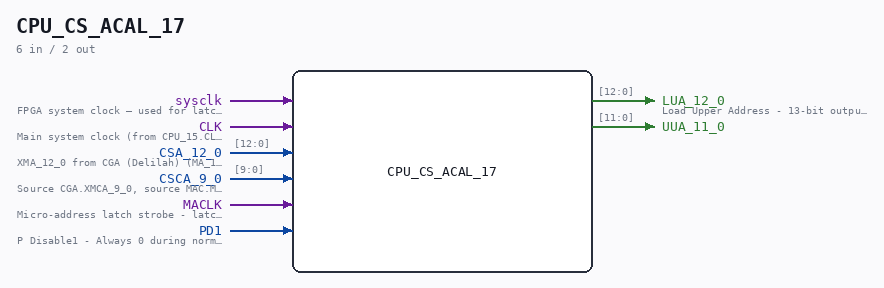
Schematic
Drawn from the Verilog: the yosys netlist of the Simulation (Verilator) build, instance CORE.CPU_BOARD.CPU.CS.ACAL. Sub-modules are boxes (click the picture to open it full size; there every sub-module box links to its page, and every wire shows its Verilog name).
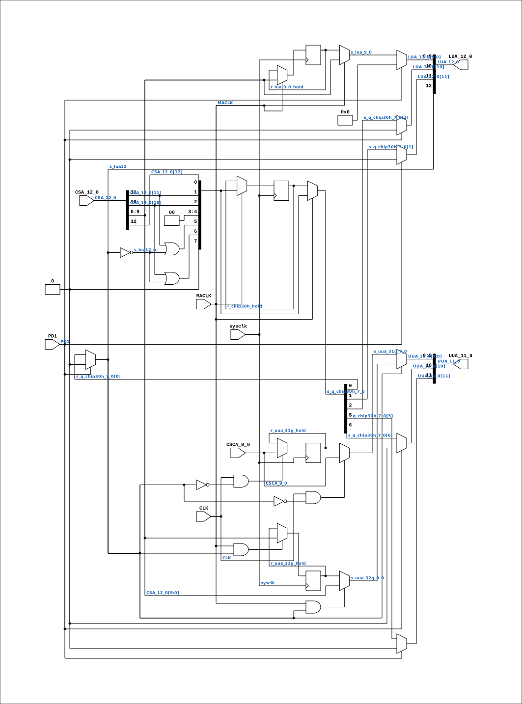
Description
ND120 CPU, MM&M CPU/CS/ACAL MICRO ADDR CALC UNIT SHEET 17 of 50 Last reviewed: 6-APR-2025 Ronny Hansen
Ports
| Direction | Width | Name | Description |
|---|---|---|---|
| input | 1 |
sysclk |
FPGA system clock — used for latch-equivalent FFs |
| input | 1 |
CLK |
Main system clock (from CPU_15.CLK) |
| input | [12:0] |
CSA_12_0 |
XMA_12_0 from CGA (Delilah) (MA_12_0 from CGA.MIC) <= Memory Address Bits (for Control Store) (from CPU_CS_16.CSA_12_0) |
| input | [9:0] |
CSCA_9_0 |
Source CGA.XMCA_9_0, source MAC.MCA_9_0, source MAC_AP09.MCA_9_0, source CALCA.MCA9_0 <= Input ICA.Bits [15:0] but only when MCLK is low. (from CPU_CS_16.CSCA_9_0) |
| input | 1 |
MACLK |
Micro-address latch strobe - latch enable for the control-store address latches in CPU_CS_ACAL_17 (transparent high, captures on the FALLING edge). (from CPU_15.MACLK) |
| input | 1 |
PD1 |
P Disable1 - Always 0 during normal operations (from CPU_CS_16.PD1) |
| output | [12:0] |
LUA_12_0 |
Load Upper Address - 13-bit output for upper address bits of control store (to CPU_CS_16.LUA_12_0) |
| output | [11:0] |
UUA_11_0 |
Verilog source
Verilog/CPU-BOARD-3202/circuit/CPU_CS_ACAL_17.v on GitHub.
Show the Verilog of CPU_CS_ACAL_17 (177 lines)
/**************************************************************************
** ND120 CPU, MM&M                                                       **
** CPU/CS/ACAL                                                           **
** MICRO ADDR CALC UNIT                                                  **
** SHEET 17 of 50                                                        **
**                                                                       **
** Last reviewed: 6-APR-2025                                             **
** Ronny Hansen                                                          **
***************************************************************************/


module CPU_CS_ACAL_17 (
    input         sysclk,   //! FPGA system clock — used for latch-equivalent FFs
    input         CLK,      //! Main system clock (from CPU_15.CLK)
    input  [12:0] CSA_12_0,  //! XMA_12_0 from CGA (Delilah) (MA_12_0 from CGA.MIC) <= Memory Address Bits (for Control Store) (from CPU_CS_16.CSA_12_0)
    input  [ 9:0] CSCA_9_0,  //! Source CGA.XMCA_9_0, source MAC.MCA_9_0, source MAC_AP09.MCA_9_0, source CALCA.MCA9_0 <= Input ICA.Bits [15:0] but only when MCLK is low. (from CPU_CS_16.CSCA_9_0)
    input         MACLK,    //! Micro-address latch strobe - latch enable for the control-store address latches in CPU_CS_ACAL_17 (transparent high, captures on the FALLING edge). (from CPU_15.MACLK)
    input         PD1,      //! P Disable1 - Always 0 during normal operations (from CPU_CS_16.PD1)
    output [12:0] LUA_12_0,  //! Load Upper Address - 13-bit output for upper address bits of control store (to CPU_CS_16.LUA_12_0)
    output [11:0] UUA_11_0
);

  /*******************************************************************************
   ** The wires and registers are defined here                                   **
   *******************************************************************************/

  // MACLK is the MICRO-ADDRESS LATCH STROBE - the latch enable for these
  // chips, and their ONLY clock. It is not a "memory access clock"; these
  // latches are its only consumer on the whole board. Confirmed against the
  // drawing (08-AUG-2026): CHIP_31F pin LE = MACLK, CHIP_30H pin C = MACLK,
  // and both output enables (/OE, /OC) = PD1. See PAL_44307C.v for the
  // equation and the naming note.
  //
  // Original chips (74373, AM29841) are TRANSPARENT LATCHES with enable.
  // When enable (MACLK) = 1: output follows input (transparent, ZERO latency).
  // When enable = 0: output holds last value (latch).
  // The capture is therefore MACLK's FALLING edge.
  //
  // CORRECTION (08-AUG-2026): the line that used to sit here claimed "during
  // execution, MACLK = 1 always (TERM_n=0), so LUA = CSA with no delay". That
  // is WRONG and was never measured. MACLK pulses once per microcycle - the
  // PAL_44307C equation asserts it only for MAP, TRAP and RWCS cases, and the
  // board's MACLK = ~(TERM_n & MACLK_n) adds only TERM. Measured in the
  // waveform, MACLK goes low mid-cycle on ordinary microwords. LUA does still
  // need to track CSA with ZERO latency while MACLK is high (see below) - that
  // part of the reasoning stands - but not because MACLK is permanently high.
  // LUA is the WCS control-store READ ADDRESS and feeds the WCS BRAM
  // combinationally, so LUA MUST track CSA with zero latency - on a microcode
  // JUMP the target's microword must be read the same cycle the address changes.
  //
  // ONE implementation for simulation and silicon (18-AUG-2026): hold-FF plus an
  // output mux. Edge-triggered storage only, no inferred latch, and zero latency
  // while the enable is high. There is deliberately no build-mode switch here -
  // what Verilator measures is what the FPGA runs.
  // HISTORY: the FPGA branch was previously a plain posedge FF+CE that lagged
  // LUA by 1 cycle. That lag corrupted CSBITS on JUMPs and was the Tang Nano 20K
  // boot hang (hang at microcode 06000 = STZ->CONT). Root-caused + fixed 19-JUL;
  // the old "1-cycle lag acceptable / ILA-confirmed" claim was WRONG.
  // Regression tests: sim/CPU_CS_ACAL_17_tb.v (asserts zero-latency transparency).

  reg [7:0]  s_q_chip30h_7_0;  // CHIP_30H: LUA[12:10], UUA[11:10]
  reg [9:0]  s_lua_9_0;        // CHIP_31F: LUA[9:0]
  reg [9:0]  s_uua_32g_9_0;   // CHIP_32G: UUA[9:0] when lua12=1
  reg [9:0]  s_uua_31g_9_0;   // CHIP_31G: UUA[9:0] when lua12=0

  wire [12:0] s_lua;
  wire [11:0] s_uua;
  wire [ 9:0] s_csca_9_0;
  wire [12:0] s_csa_12_0;
  wire [ 7:0] s_d_chip30h_7_0;
  wire        s_lua12;
  wire        s_lua12_n;
  wire        s_pd1;
  (* mark_debug = "true", DONT_TOUCH = "true" *) wire s_maclk;
  wire        s_clk;

  /*******************************************************************************
   ** Wiring                                                                     **
   *******************************************************************************/

  // LUA[12:10] from CHIP_30H registered output
  assign s_lua[12] = s_pd1 ? 1'b0 : s_q_chip30h_7_0[0];
  assign s_lua[11] = s_pd1 ? 1'b0 : s_q_chip30h_7_0[1];
  assign s_lua[10] = s_pd1 ? 1'b0 : s_q_chip30h_7_0[2];

  // LUA[9:0] from CHIP_31F registered output
  assign s_lua[9:0] = s_pd1 ? 10'b0 : s_lua_9_0;

  // UUA[11:10] from CHIP_30H registered output
  assign s_uua[11] = s_pd1 ? 1'b0 : s_q_chip30h_7_0[5];
  assign s_uua[10] = s_pd1 ? 1'b0 : s_q_chip30h_7_0[6];

  // UUA[9:0]: CHIP_32G when lua12=1, CHIP_31G when lua12=0
  assign s_uua[9:0] = s_lua12 ? s_uua_32g_9_0 : s_uua_31g_9_0;

  // CHIP_30H D inputs (same logic as original)
  assign s_d_chip30h_7_0[0] = s_csa_12_0[12];
  assign s_d_chip30h_7_0[1] = s_csa_12_0[11];
  assign s_d_chip30h_7_0[2] = s_csa_12_0[10];
  assign s_d_chip30h_7_0[3] = 1'b0;  // not used
  assign s_d_chip30h_7_0[4] = 1'b0;  // not used
  assign s_d_chip30h_7_0[5] = s_csa_12_0[11] | s_lua12_n;
  assign s_d_chip30h_7_0[6] = s_csa_12_0[10] | s_lua12_n;
  assign s_d_chip30h_7_0[7] = 1'b0;

  assign s_lua12   = s_lua[12];
  assign s_lua12_n = ~s_lua12;

  // Unused CHIP_30H bits — keep for linter
  (* keep = "true", DONT_TOUCH = "true" *) wire [2:0] unused_CHIP30h_bits;
  assign unused_CHIP30h_bits = {s_q_chip30h_7_0[7], s_q_chip30h_7_0[4], s_q_chip30h_7_0[3]};

  /*******************************************************************************
   ** Inputs / Outputs                                                           **
   *******************************************************************************/
  assign s_csca_9_0  = CSCA_9_0;
  assign s_csa_12_0  = CSA_12_0;
  assign s_pd1       = PD1;
  assign s_maclk     = MACLK;
  assign s_clk       = CLK;

  assign LUA_12_0    = s_lua[12:0];
  assign UUA_11_0    = s_uua[11:0];

  /*******************************************************************************
   ** Latch logic - ONE implementation, identical for Verilator and silicon      **
   *******************************************************************************/

// 18-AUG-2026: the transparent-latch branch that used to live here is DELETED.
//
// It was selected by a bare VERILATOR_SIM test, so EVERY Verilator build took it
// - including builds compiled with -DFPGA_FF_MODE. FPGA_FF_MODE never reached
// this module at all, which meant "FF-mode" simulations were still executing
// four real transparent latches while the FPGA executed flip-flops. Sim and
// silicon were running DIFFERENT HARDWARE, and this is the worst module for that
// to happen in: ACAL is where the TRAP VECTOR is captured (PAL_44307C.v:119,
// MACLK "d+e CAPTURE TRAP VECTOR"), i.e. exactly the path a page fault must take
// to reach the microcode.
//
// There is now ONE implementation below and no build-mode switch, so whatever is
// measured in Verilator is what runs on the FPGA. Do not reintroduce a
// simulation-only variant of this logic.
//
// Note on what "flip-flops" means here: the pair below is a hold flip-flop plus
// an output mux. It is entirely edge-triggered storage - no latch is inferred
// (verified: verilator lint with -Wno-LATCH REMOVED reports zero LATCH warnings)
// - while still presenting the zero-latency transparency the original 74373 and
// AM29841 chips had. That transparency is load-bearing: a plain posedge FF
// without it was tried on 19-JUL-2026 and hung the CPU, because LUA lagged the
// control-store read address by one cycle, the WCS returned the wrong microword,
// and the sequencer jumped to 16000 instead of 0145 and stuck at 06000 forever.
  // Hold-FF + output mux. Captures on posedge sysclk when the enable is high;
  // the mux passes the input through while the enable is high and holds the
  // captured value otherwise. Edge-triggered storage only - no inferred latch.

  reg [7:0] r_chip30h_hold;
  reg [9:0] r_lua_9_0_hold;
  reg [9:0] r_uua_32g_hold;
  reg [9:0] r_uua_31g_hold;

  // CHIP_30H: 74373 transparent latch, enable=MACLK
  always @(posedge sysclk) if (s_maclk) r_chip30h_hold <= s_d_chip30h_7_0;
  always @(*) s_q_chip30h_7_0 = s_maclk ? s_d_chip30h_7_0 : r_chip30h_hold;

  // CHIP_31F: AM29841 transparent latch, enable=MACLK
  always @(posedge sysclk) if (s_maclk) r_lua_9_0_hold <= s_csa_12_0[9:0];
  always @(*) s_lua_9_0 = s_maclk ? s_csa_12_0[9:0] : r_lua_9_0_hold;

  // CHIP_32G: AM29841 transparent latch, enable=MACLK && lua12
  always @(posedge sysclk) if (s_maclk && s_lua12) r_uua_32g_hold <= s_csa_12_0[9:0];
  always @(*) s_uua_32g_9_0 = (s_maclk && s_lua12) ? s_csa_12_0[9:0] : r_uua_32g_hold;

  // CHIP_31G: AM29841 transparent latch, enable=CLK && !lua12
  always @(posedge sysclk) if (s_clk && ~s_lua12) r_uua_31g_hold <= s_csca_9_0[9:0];
  always @(*) s_uua_31g_9_0 = (s_clk && ~s_lua12) ? s_csca_9_0[9:0] : r_uua_31g_hold;

endmodule