CPU_MMU_24
Source: Verilog/CPU-BOARD-3202/circuit/CPU_MMU_24.v
Where it sits (Simulation): ND120_TOP > ND120_CORE > ND3202D > CPU_15 > CPU_MMU_24
- instance path: CORE.CPU_BOARD.CPU.MMU
Used in: CPU_15 (all tops)
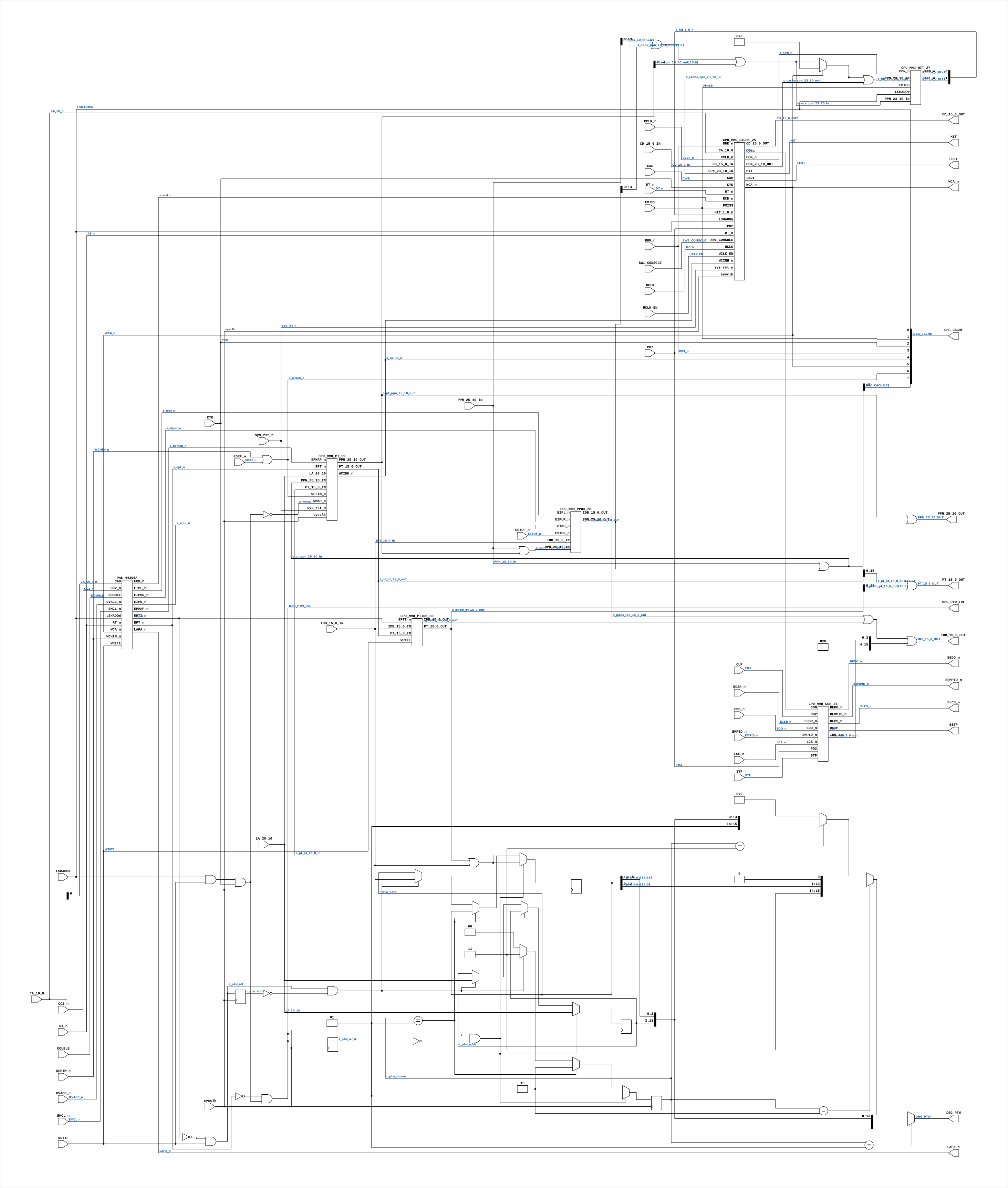
Contains: CPU_MMU_CACHE_25, CPU_MMU_CSR_26, CPU_MMU_HIT_27, CPU_MMU_PPNX_28, CPU_MMU_PT_29, CPU_MMU_PTIDB_30, PAL_44306A
Module hierarchy - All modules
Schematic
Drawn from the Verilog: the yosys netlist of the Simulation (Verilator) build, instance CORE.CPU_BOARD.CPU.MMU. Sub-modules are boxes (click the picture to open it full size; there every sub-module box links to its page, and every wire shows its Verilog name).
Description
ND120 CPU, MM&M CPU/MMU MMU TOP LEVEL SHEET 24 of 50 Last reviewed: 2-FEB-2025 Ronny Hansen
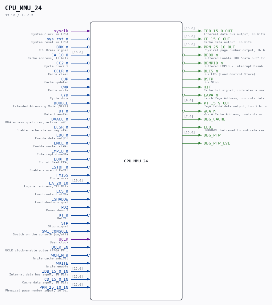
Ports
| Direction | Width | Name | Description |
|---|---|---|---|
| input | 1 |
sysclk |
System clock in FPGA |
| input | 1 |
sys_rst_n (active low) |
System reset in FPGA |
| input | 1 |
BRK_n (active low) |
CPU Break signal |
| input | [10:0] |
CA_10_0 |
Cache address, 11 bits |
| input | 1 |
CC2_n (active low) |
Cycle clock 2 |
| input | 1 |
CCLR_n (active low) |
Cache clear |
| input | 1 |
CUP |
Cache updated |
| input | 1 |
CWR |
Cache write |
| input | 1 |
CYD |
Cycle done |
| input | 1 |
DOUBLE |
Extended Adressing Mode (SEXI) |
| input | 1 |
DT_n (active low) |
Data transfer |
| input | 1 |
DVACC_n (active low) |
DGA access qualifier, active low (see comment above) |
| input | 1 |
ECSR_n (active low) |
Enable cache status register |
| input | 1 |
EDO_n (active low) |
Enable data output |
| input | 1 |
EMCL_n (active low) |
Enable master clear |
| input | 1 |
EMPID_n (active low) |
Interrupt disable |
| input | 1 |
EORF_n (active low) |
End of Read Flag |
| input | 1 |
ESTOF_n (active low) |
Enable store of Fault |
| input | 1 |
FMISS |
Force miss |
| input | [10:0] |
LA_20_10 |
Logical address, 11 bits |
| input | 1 |
LCS_n (active low) |
Load control store |
| input | 1 |
LSHADOW |
Load shadow signal |
| input | 1 |
PD2 |
Power down 2 |
| input | 1 |
RT_n (active low) |
Return |
| input | 1 |
STP |
Stop signal |
| input | 1 |
SW1_CONSOLE |
Switch on the console (on/off) |
| input | 1 |
UCLK |
User clock |
| input | 1 |
UCLK_EN |
UCLK clock-enable pulse (FPGA_FF_MODE, else 0) |
| input | 1 |
WCHIM_n (active low) |
Write cache inhibit |
| input | 1 |
WRITE |
Write enable |
| input | [15:0] |
IDB_15_0_IN |
Internal data bus input, 16 bits |
| output | [15:0] |
IDB_15_0_OUT |
Internal data bus output, 16 bits |
| input | [15:0] |
CD_15_0_IN |
Cache data input, 16 bits |
| output | [15:0] |
CD_15_0_OUT |
Cache data output, 16 bits |
| input | [15:0] |
PPN_25_10_IN |
Physical page number input, 16 bits |
| output | [15:0] |
PPN_25_10_OUT |
Physical page number output, 16 bits |
| output | 1 |
BEDO_n (active low) |
Buffered Enable IDB "data out" from CGA |
| output | 1 |
BEMPID_n (active low) |
Buffered EMPID - Interrupt Disable (EPIC.LDMPIE->set mask reg:inh all ints) |
| output | 1 |
BLCS_n (active low) |
Bus LCS (Load Control Store) |
| output | 1 |
BSTP |
Bus Stop |
| output | 1 |
HIT |
Cache hit signal, indicates a successful cache lookup |
| output | 1 |
LAPA_n (active low) |
Latch Page Address, controls latching of the page address |
| output | [6:0] |
PT_15_9_OUT |
Page Table data output, top 7 bits |
| output | 1 |
WCA_n (active low) |
Write Cache Address, controls writing to the cache address register |
| output | [7:0] |
DBG_CACHE |
|
| output | 1 |
LED1 |
UNKNOWN: believed to indicate cache enabled, never traced. See Verilog/docs/SIGNALS.md |
| output | [15:0] |
DBG_PTW |
|
| output | 1 |
DBG_PTW_LVL |
Verilog source
Verilog/CPU-BOARD-3202/circuit/CPU_MMU_24.v on GitHub.
Show the Verilog of CPU_MMU_24 (665 lines)
/**************************************************************************
** ND120 CPU, MM&M                                                       **
** CPU/MMU                                                               **
** MMU TOP LEVEL                                                         **
** SHEET 24 of 50                                                        **
**                                                                       **
** Last reviewed: 2-FEB-2025                                             **
** Ronny Hansen                                                          **
***************************************************************************/

module CPU_MMU_24 (
    input sysclk,    // System clock in FPGA
    input sys_rst_n, // System reset in FPGA

    input        BRK_n,          //! CPU Break signal
    input [10:0] CA_10_0,        //! Cache address, 11 bits
    input        CC2_n,          //! Cycle clock 2
    input        CCLR_n,         //! Cache clear
    input        CUP,            //! Cache updated
    input        CWR,            //! Cache write
    input        CYD,            //! Cycle done
    input        DOUBLE,         //! Extended Adressing Mode (SEXI)
    input        DT_n,           //! Data transfer
    // DVACC_n comes from the DECODER gate array (DECODE_DGA_COMM.v flip-flop
    // A227 on CLK2) via IO_37, and is the access qualifier for the page-table
    // control PAL below: PAL_44306A uses it (input I2) together with WRITE,
    // DOUBLE, WCA_n and LSHADOW to decide ECD_n / LAPA_n, i.e. when the page
    // table is actually addressed. NOT the CGA's VACC (CGA_DCD.v) - different
    // net, same name.
    input        DVACC_n,        //! DGA access qualifier, active low (see comment above)
    input        ECSR_n,         //! Enable cache status register
    input        EDO_n,          //! Enable data output
    input        EMCL_n,         //! Enable master clear
    input        EMPID_n,        //! Interrupt disable
    input        EORF_n,         //! End of Read Flag
    input        ESTOF_n,        //! Enable store of Fault
    input        FMISS,          //! Force miss
    input [10:0] LA_20_10,       //! Logical address, 11 bits
    input        LCS_n,          //! Load control store
    input        LSHADOW,        //! Load shadow signal
    input        PD2,            //! Power down 2
    input        RT_n,           //! Return
    input        STP,            //! Stop signal
    input        SW1_CONSOLE,    //! Switch on the console (on/off)
    input        UCLK,           //! User clock
    input        UCLK_EN,        //! UCLK clock-enable pulse (FPGA_FF_MODE, else 0)
    input        WCHIM_n,        //! Write cache inhibit
    input        WRITE,          //! Write enable

    input  [15:0] IDB_15_0_IN,   //! Internal data bus input, 16 bits
    output [15:0] IDB_15_0_OUT,  //! Internal data bus output, 16 bits

    input  [15:0] CD_15_0_IN,    //! Cache data input, 16 bits
    output [15:0] CD_15_0_OUT,   //! Cache data output, 16 bits

    input  [15:0] PPN_25_10_IN,  //! Physical page number input, 16 bits
    output [15:0] PPN_25_10_OUT, //! Physical page number output, 16 bits

    output BEDO_n,               //! Buffered Enable IDB "data out" from CGA
    output BEMPID_n,             //! Buffered EMPID - Interrupt Disable (EPIC.LDMPIE->set mask reg:inh all ints)
    output BLCS_n,               //! Bus LCS (Load Control Store)
    output BSTP,                 //! Bus Stop
    output HIT,                  //! Cache hit signal, indicates a successful cache lookup
    output LAPA_n,               //! Latch Page Address, controls latching of the page address
    output [6:0] PT_15_9_OUT,    //! Page Table data output, top 7 bits
    output WCA_n,                //! Write Cache Address, controls writing to the cache address register
    //! DBG_CACHE - the six signals that gate a cache write, brought out so an
    //! ILA can say which one is actually blocking it. Added 28-AUG-2026.
    //!
    //! WHY. On the Nexys 4 DDR the machine's own diagnostic CACHE-1X0-A00,
    //! test 2, reports the cache totally inert: data and instructions are
    //! never COPIED INTO the cache when read, and never TAKEN FROM it when
    //! present, both with paging off and on. Nothing is ever written, so
    //! nothing can ever hit, so CUP never sets.
    //!
    //! A cache write happens when PAL_44402D asserts WCA, and its PALASM
    //! (DesignDocuments/PAL-Code/SRC/44402D.txt) says
    //!
    //!   WCA = /RT * DT * EWC * CYD * /FMISS * /LSHADOW
    //!       + RT * /IHIT * EWC * CYD * /FMISS * /LSHADOW
    //!
    //! Both terms need EWC and CYD high and FMISS and LSHADOW low. The PAL
    //! itself is transcribed correctly - checked against that listing on
    //! 28-AUG-2026, both product terms and the registered/combinational split
    //! (WCA is "=", combinational; only IHIT/NUBI/NUBD are ":=" - which is
    //! exactly the mistake that had been made in PAL_44511A). CON is tied
    //! high in ND120_CORE.v, so it is not the blocker either. That leaves one
    //! of WCINH_n, BRK_n, CYD, FMISS or LSHADOW, and reading the source
    //! cannot choose between them - it has to be measured while it runs.
    //!
    //! FMISS is the standing suspect: it comes off flip-flop A160 in
    //! DECODE_DGA_COMM.v, whose D input runs back through A177 =
    //! NAND(LCS_n, MREQ, FMISS) - a self-hold. Once FMISS sets it stays set
    //! while MREQ is asserted, and the PAL's own history note says "WCA
    //! SHOULD NOT APPEAR WHEN FMISS (TSET FAILS)". SUSPECT, NOT VERIFIED.
    //!
    //! Bit layout, low to high:
    //!   [0] LSHADOW  [1] FMISS  [2] CYD  [3] BRK_n  [4] WCINH_n  [5] WCA_n
    //!   [6] WCLIM_n - inhibit-RAM write strobe (added after the first capture)
    //!   [7] PPN25 - the DATA being written into the inhibit RAM (second capture)
    output [7:0] DBG_CACHE,
    output LED1,                 //! UNKNOWN: believed to indicate cache enabled, never traced. See Verilog/docs/SIGNALS.md
    //! DEBUG: page-table WRITE stream (23-AUG-2026, zero-read campaign).
    //! On every PT-chip write strobe (EPT_n low & WMAP_n low) two words are
    //! emitted on consecutive sysclks, 16'h0000 otherwise:
    //!   word A = {2'b10, addr[10:0], data[15:13]}   (addr = LA_20_10 index)
    //!   word B = {2'b11, data[12:0], 1'b0}
    //! Same pattern as MEM_43's DBG_MEMW; consumed by TANG_PTWR_CAPTURE.
    output [15:0] DBG_PTW,
    //! DEBUG level (27-AUG, wrong-PPN option-1 probe): PT-chip write strobe
    //! conjunction LIVE (~EPT_n & ~WMAP_n) - unlike DBG_PTW's edge-detected
    //! stream, this stays high for the WHOLE elongated strobe, so the top
    //! can AND it with MEM_HOLD to measure write-during-freeze overlap.
    output DBG_PTW_LVL
);


  /*******************************************************************************
   ** The wires are defined here                                                 **
   *******************************************************************************/
  wire [10:0] s_la_20_10;
  wire [15:0] s_idb_15_0_out;

  wire [13:0] s_hit_cpn_23_10_in;
  wire [10:0] s_ca_10_0;

  wire [ 1:0] s_hit_1_0_n;

  wire        s_ecd_n;
  wire        s_bstp;
  wire        s_bedo_n;
  wire        s_con;
  wire        s_ept_n;
  wire        s_empid_n;
  wire        s_lcs_n;
  wire        s_ecsr_n;
  wire        s_lapa_n;
  wire        s_wclim_n;
  wire        s_uclk;
  wire        s_cwr;
  wire        s_wchim_n;
  wire        s_hit;
  wire        s_eipur_n;
  wire        s_eipl_n;
  wire        s_con_n;
  wire        s_cyd;
  wire        s_pd2;
  wire        s_sw1_console;
  wire        s_wcinh_n;
  wire        s_eipu_n;
  wire        s_eorf_n;
  wire        s_epmap_n;
  wire        s_estof_n;
  wire        s_cup;
  wire        s_dvacc_n;
  wire        s_emcl_n;
  wire        s_epti_n;
  wire        s_bempid_n;
  wire        s_blcs_n;
  wire        s_stp;
  wire        s_edo_n;
  wire        s_dt_n;
  wire        s_brk_n;
  wire        s_wmap_n;
  wire        s_rt_n;
  wire        s_cc2_n;
  wire        s_cclr_n;
  wire        s_fmiss;
  wire        s_double;
  wire        s_write;
  wire        s_lshadow;
  wire        s_wca_n;
  wire        s_led1;

  // PPN
  wire [15:0] s_ppn_25_10_in;

  // PT
  // PT PPN
  wire [15:0] s_pt_ppn_25_10_out;
  wire [15:0] s_pt_ppn_25_10_in;

  // PT PT
  wire [15:0] s_pt_pt_15_0_out;
  wire [15:0] s_pt_pt_15_0_in;


  // CPN
  wire [13:0] s_cache_cpn_23_10_out;
  wire [13:0] s_cache_cpn_23_10_in;

  wire [15:0] s_cache_cd_15_0_in;
  wire [15:0] s_cache_cd_15_0_out;

  // PTIDB
  wire [15:0] s_ptidb_pt_15_0_in;
  wire [15:0] s_ptidb_pt_15_0_out;

  wire [15:0] s_ptidb_idb_15_0_in;
  wire [15:0] s_ptidb_idb_15_0_out;

  // PPNX
  wire [15:0] s_ppnx_idb_15_0_in;
  wire [15:0] s_ppnx_idb_15_0_out;

  wire [15:0] s_ppnx_ppn_25_10_in;
  wire [15:0] s_ppnx_ppn_25_10_out;

  // WCA
  wire [13:0] s_wca_ppn_23_10_in;
  wire [13:0] s_wca_cpn_23_10_out;

  // CSR
  wire [ 3:0] s_csr_idb_3_0_out;

  /*******************************************************************************
   ** Here all input connections are defined                                     **
   *******************************************************************************/


  assign s_la_20_10[10:0] = LA_20_10;
  assign s_ca_10_0[10:0] = CA_10_0;
  assign s_empid_n = EMPID_n;
  assign s_lcs_n = LCS_n;
  assign s_ecsr_n = ECSR_n;
  assign s_uclk = UCLK;
  assign s_cwr = CWR;
  assign s_wchim_n = WCHIM_n;
  assign s_cyd = CYD;
  //! See the DBG_CACHE port comment for what this bus is and why it exists.
  //! Bit 6 is WCLIM_n, added 29-AUG-2026 after the first capture. That one
  //! measured WCINH_n LOW - the page marked cache-inhibited - in 914 of 1024
  //! samples, while FMISS and LSHADOW were 0 throughout and WCA_n did fire
  //! whenever WCINH_n happened to be high. So the inhibit BIT is the question
  //! now, and the first half of it is whether the inhibit RAM is ever written
  //! at all: IMS1403_25 has no reset (the commented-out loop there says Vivado
  //! would not take one), so an untouched cell reads whatever the block RAM
  //! powers up as - which would produce "inhibited nearly everywhere" with the
  //! CPU never involved. WCLIM_n is that RAM's write strobe, so triggering on
  //! it going low says directly whether anything ever writes the bit.
  //! Bit 7 is the DATA the inhibit RAM is being written with - PPN bit 25 on
  //! the bus that addresses CHIP_20G. Added 29-AUG-2026 after the WCLIM_n
  //! capture, which proved the RAM IS written (69 write strobes in one
  //! 1024-sample window), killing the "it is just uninitialised block RAM"
  //! theory. So the bit is written and it still reads INHIBITED almost
  //! everywhere, and the question becomes what value is going in.
  //!
  //! It cannot be read off WCINH_n. IMS1403_25.v:34 is
  //!     assign Q = (!CE_n && W_n) ? data_out : 1'b0;
  //! so the RAM's output is FORCED LOW for the whole of a write. Every one of
  //! those 69 samples showed WCINH_n = 0 for that reason alone, and reading
  //! "inhibited" from them would be reading the model's own artefact.
  //! Sampling the data input is the only way to see what is stored.
  assign DBG_CACHE = {s_pt_ppn_25_10_in[15], s_wclim_n, s_wca_n, s_wcinh_n,
                      s_brk_n, s_cyd, s_fmiss, s_lshadow};
  assign s_pd2 = PD2;
  assign s_sw1_console = SW1_CONSOLE;
  assign s_eorf_n = EORF_n;
  assign s_estof_n = ESTOF_n;
  assign s_cup = CUP;
  assign s_dvacc_n = DVACC_n;
  assign s_emcl_n = EMCL_n;
  assign s_stp = STP;
  assign s_edo_n = EDO_n;
  assign s_dt_n = DT_n;
  assign s_brk_n = BRK_n;
  assign s_rt_n = RT_n;
  assign s_cc2_n = CC2_n;
  assign s_cclr_n = CCLR_n;
  assign s_fmiss = FMISS;
  assign s_double = DOUBLE;
  assign s_write = WRITE;
  assign s_lshadow = LSHADOW;
  assign s_ppn_25_10_in = PPN_25_10_IN;
  assign s_cache_cd_15_0_in = CD_15_0_IN;

  /*******************************************************************************
   ** Here all output connections are defined                                    **
   *******************************************************************************/
  assign BEDO_n = s_bedo_n;
  assign BEMPID_n = s_bempid_n;
  assign BLCS_n = s_blcs_n;
  assign BSTP = s_bstp;
  assign CD_15_0_OUT = s_cache_cd_15_0_out[15:0];
  assign HIT = s_hit;
  assign IDB_15_0_OUT = s_idb_15_0_out[15:0];
  assign LAPA_n = s_lapa_n;
  assign PPN_25_10_OUT = s_pt_ppn_25_10_out | s_ppnx_ppn_25_10_out;
  assign PT_15_9_OUT = s_pt_pt_15_0_out[15:9] | s_ptidb_pt_15_0_out[15:9];
  assign WCA_n = s_wca_n;
  assign LED1 = s_led1;

  // Connect PT[15:0] between PT and PDIDB components
  assign s_pt_pt_15_0_in = s_ptidb_pt_15_0_out | s_ptidb_idb_15_0_in;
  assign s_ptidb_pt_15_0_in = s_pt_pt_15_0_out;

  // Connect PPN INPUT signals from PPN IN or with (PT or PPNX out)
  assign s_pt_ppn_25_10_in = s_ppn_25_10_in | s_ppnx_ppn_25_10_out;
  assign s_ppnx_ppn_25_10_in = s_ppn_25_10_in | s_pt_ppn_25_10_out;

  // Assign input and output signals for IDB
  assign s_ptidb_idb_15_0_in = IDB_15_0_IN;
  assign s_ppnx_idb_15_0_in = IDB_15_0_IN;

  assign s_idb_15_0_out[15:0] =
        s_ppnx_idb_15_0_out  |
        s_ptidb_idb_15_0_out |
        {12'b0, s_csr_idb_3_0_out[3:0]};


  // BUS SIGNALS
  assign s_wca_ppn_23_10_in =
         s_ppn_25_10_in[13:0]       | // Input to module
         s_ppnx_ppn_25_10_out[13:0] |  // output from PPNX module
         s_pt_ppn_25_10_out[13:0];     // output from PPN module

  /*******************************************************************************
   ** Here all normal components are defined                                     **
   *******************************************************************************/
  assign s_wclim_n = s_wchim_n | s_eorf_n;
  assign s_wmap_n = ~(s_lshadow & s_write & s_cyd);

  /*******************************************************************************
   ** Here all sub-circuits are defined                                          **
   *******************************************************************************/

  // HIT DETECTOR MODULE: This module, CPU_MMU_HIT_27, is responsible for determining cache hit status.
  // It compares the provided physical page number (PPN) and cache page number (CPN) inputs to detect
  // if there is a match, indicating a cache hit. The module takes in 14-bit inputs for both PPN and CPN,
  // along with control signals LSHADOW, FMISS, and CON_n. It outputs two signals, HIT0_n and HIT1_n,
  // which represent the negated hit status for different conditions. A low output on these signals
  // indicates a cache hit, while a high output indicates a miss.
  CPU_MMU_HIT_27 MMU_HIT
  (
    // Input signals
    .CPN_23_10_IN(s_hit_cpn_23_10_in[13:0]),
    // The PPN(25:10) bus on sheet 24 is ONE node: the PT map RAM output, the
    // PPNX output and the external PPN input all sit on it, and the vertical
    // into the HIT block drops off that shared bus. This passed only
    // s_ppn_25_10_in, which per CPU_15.v:391-393 is the LAPA latch alone and
    // is ZERO whenever LAPA~ is high - i.e. on every MAPPED access. So the
    // cache hit decision for paged memory was made by comparing the stored
    // tag against a constant 0. s_wca_ppn_23_10_in (built at :234-237) is the
    // same merge the WCA feed already uses, and is the bus the drawing shows.
    .PPN_23_10_IN(s_wca_ppn_23_10_in[13:0]),

    .LSHADOW(s_lshadow),
    .FMISS  (s_fmiss),
    .CON_n  (s_con_n),

    // Output signals
    .HIT0_n(s_hit_1_0_n[0]),
    .HIT1_n(s_hit_1_0_n[1])
  );

  // The CPU_MMU_PPNX_28 module is responsible for handling the translation and manipulation
  // of the Physical Page Number (PPN) and the Internal Data Bus (IDB) signals. It takes in
  // control signals such as EIPL_n, EIPUR_n, EIPU_n, and ESTOF_n to determine the direction
  // and conditions under which data is transferred between the PPN and IDB. The module
  // outputs the modified PPN and IDB values, facilitating the interaction between the
  // memory management unit and other components of the CPU.
  CPU_MMU_PPNX_28 PPNX
  (
    // Input signals
    .EIPL_n(s_eipl_n),
    .EIPUR_n(s_eipur_n),
    .EIPU_n(s_eipu_n),
    .ESTOF_n(s_estof_n),

     // Bus signals (in and out)
    .IDB_15_0_IN(s_ppnx_idb_15_0_in[15:0]),
    .IDB_15_0_OUT(s_ppnx_idb_15_0_out[15:0]),

    .PPN_25_10_IN(s_ppnx_ppn_25_10_in[15:0]),
    .PPN_25_10_OUT(s_ppnx_ppn_25_10_out[15:0])
  );

  // The CPU_MMU_PTIDB_30 module is responsible for interfacing between the Page Table (PT) and the Internal Data Bus (IDB).
  // It manages the data flow between these components, allowing for the reading and writing of page table entries.
  // The module takes in control signals such as EPTI_n and WRITE to determine the operation mode, and it handles
  // 16-bit data inputs and outputs for both the IDB and PT. This module is crucial for maintaining the integrity
  // and efficiency of memory management operations within the CPU.
  CPU_MMU_PTIDB_30 PTIDB
  (
    .WRITE(s_write), // Direction
    .EPTI_n(s_epti_n), // Output enable

    // Bus signals (in and out)
    .IDB_15_0_IN(s_ptidb_idb_15_0_in[15:0]),
    .IDB_15_0_OUT(s_ptidb_idb_15_0_out[15:0]),

    .PT_15_0_IN(s_ptidb_pt_15_0_in),
    .PT_15_0_OUT(s_ptidb_pt_15_0_out)
  );


  // CPU_MMU_WCA_31.v is replaced by this line
  // if s_lapa_n is high, output is high-impedance
  assign s_wca_cpn_23_10_out[13:0] = s_wca_n ? 14'b0 : s_wca_ppn_23_10_in[13:0];

  // Combine the CPN output from WCA and CACHE
  assign s_hit_cpn_23_10_in = s_wca_cpn_23_10_out | s_cache_cpn_23_10_out;

  // Assign the correct bits to the CACHE cpn in bits
  assign s_cache_cpn_23_10_in = s_wca_cpn_23_10_out;

  // Cache Status Register (CSR)
  //
  // The CPU_MMU_CSR_26 module serves as the Cache Status Register (CSR) within the Memory Management Unit (MMU).
  // It is responsible for managing and outputting various status signals related to cache operations.
  // The module takes several input signals, including STP, EMPID_n, EDO_n, LCS_n, PD2, CUP, CON, and ECSR_n,
  // which represent different control and status conditions of the CPU and cache system.
  // Based on these inputs, the CSR module generates output signals such as BSTP, BEMPID_n, BEDO_n, BLCS_n,
  // and a 4-bit IDB output (IDB_3_0), which are used to control and monitor the cache's behavior and status.
  CPU_MMU_CSR_26 CSR
  (
    // Input signals
    .STP(s_stp),
    .EMPID_n(s_empid_n),
    .EDO_n(s_edo_n),
    .LCS_n(s_lcs_n),
    .PD2(s_pd2),

    .CUP(s_cup),
    .CON(s_con),
    .ECSR_n(s_ecsr_n),

    // Output signals
    .BSTP(s_bstp),
    .BEMPID_n(s_bempid_n),
    .BEDO_n(s_bedo_n),
    .BLCS_n(s_blcs_n),
    .IDB_3_0(s_csr_idb_3_0_out[3:0])
  );

  // Cache
  //
  // The CPU_MMU_CACHE_25 module is responsible for managing the cache operations within the Memory Management Unit (MMU).
  // It interfaces with various input signals such as system clock, reset, and control signals like BRK_n, CWR, and FMISS,
  // which are crucial for cache control and data flow. The module handles both input and output bus signals, including
  // CD_15_0 and CPN_23_10, to facilitate data transfer between the cache and other components. Additionally, it generates
  // output signals like CON, HIT, and LED1, which indicate the cache's operational status and hit/miss results. This module
  // plays a vital role in optimizing memory access times by storing frequently accessed data, thereby improving overall
  // system performance.
  CPU_MMU_CACHE_25 CACHE
  (
    .sysclk   (sysclk),    // System clock in FPGA
    .sys_rst_n(sys_rst_n), // System reset in FPGA

    // Input signals
    .BRK_n(s_brk_n),
    .CA_10_0(s_ca_10_0[10:0]),
    .CCLR_n(s_cclr_n),
    .CWR(s_cwr),
    .CYD(s_cyd),
    .DT_n(s_dt_n),
    .ECD_n(s_ecd_n),
    .FMISS(s_fmiss),
    .HIT_1_0_n(s_hit_1_0_n[1:0]),
    .LSHADOW(s_lshadow),
    .PD2(s_pd2),
    .RT_n(s_rt_n),
    .SW1_CONSOLE(s_sw1_console),
    .UCLK(s_uclk),
    .UCLK_EN(UCLK_EN),
    .WCINH_n(s_wcinh_n),

    // Bus signals (in and out)
    .CD_15_0_IN(s_cache_cd_15_0_in),
    .CD_15_0_OUT(s_cache_cd_15_0_out),

    .CPN_23_10_IN(s_cache_cpn_23_10_in[13:0]),
    .CPN_23_10_OUT(s_cache_cpn_23_10_out[13:0]),

    // Output signals
    .CON(s_con),
    .CON_n(s_con_n),
    .HIT(s_hit),
    .WCA_n(s_wca_n),
    .LED1(s_led1)
  );

  // The PAL_44306A module, labeled as PAL_44306_UNOCTL, is a programmable array logic component
  // that manages various control signals within the Memory Management Unit (MMU). It takes multiple
  // input signals, such as cache address, write enable, and data valid acknowledge, to generate
  // specific output control signals. These outputs, like ECD_n and LAPA_n, are crucial for coordinating
  // the operations of the MMU, including enabling or disabling certain functions and managing data flow.
  // The module plays a key role in ensuring the correct sequencing and control of memory operations.
  PAL_44306A PAL_44306_UNOCTL (
      .EIPUR_n(s_eipur_n),     //B0
      .EIPU_n (s_eipu_n),      //B1
      .EIPL_n (s_eipl_n),      //B2
      .EPTI_n (s_epti_n),      //B3
      .EPMAP_n(s_epmap_n),     //B4
      .EPT_n  (s_ept_n),       //B5
      .CA0    (s_ca_10_0[0]),  //I0
      .WRITE  (s_write),       //I1
      .DVACC_n(s_dvacc_n),     //I2
      .RT_n   (s_rt_n),        //I3
      .WCHIM_n(s_wchim_n),     //I4
      .DOUBLE (s_double),      //I5
      .EMCL_n (s_emcl_n),      //I6
      .CC2_n  (s_cc2_n),       //I7
      .WCA_n  (s_wca_n),       //I8
      .LSHADOW(s_lshadow),     //I9
      .ECD_n  (s_ecd_n),       //Y0
      .LAPA_n (s_lapa_n)       //Y1
  );

  // Page Table (PT)
  //
  // This module, CPU_MMU_PT_29, is responsible for managing the Page Table (PT) operations within the Memory Management Unit (MMU).
  // It interfaces with the system clock and reset signals to ensure synchronized operations.
  // The module handles 11-bit addressing for PT chips, enabling or disabling the EPMAP and PT chips based on control signals.
  // It manages write operations to RAM chips, specifically targeting the high bit of the Page Physical Number (PPN).
  // The module also processes bidirectional signals for both PPN and PT data buses, facilitating data flow in and out.
  // Additionally, it outputs a write control inhibit signal, which is active low, to regulate write operations.
  CPU_MMU_PT_29 PT
  (
    // Inputs
    .sysclk(sysclk),             // System clock in FPGA
    .sys_rst_n(sys_rst_n),       // System reset in FPGA
    .LA_20_10(s_la_20_10[10:0]), // 11 bit addressing into PT chips
    .EPMAP_n(s_epmap_n),         // Enable EPMAP chips (Extended map?)
    .EPT_n(s_ept_n),             // Enable PT chips (Chip select for PT chips)
    .WCLIM_n(s_wclim_n),         // Write to RAM chip with 1 bit Data being PPN hi bit (bit ppn 25)
    .WMAP_n(s_wmap_n),           // Write MAPPING signal

    // Bus signals (in and out)
    .PPN_25_10_IN(s_pt_ppn_25_10_in[15:0]), // Bidirectional PPN (in)
    .PPN_25_10_OUT(s_pt_ppn_25_10_out[15:0]), // Bidirectional PPN (out)

    .PT_15_0_IN(s_pt_pt_15_0_in), // Bidirectional PT (in)
    .PT_15_0_OUT(s_pt_pt_15_0_out), // Bidirectional PT (out)

    // Outputs
    .WCINH_n(s_wcinh_n)         // Write control inhibit (active low)
  );

  // ---- DBG_PTW: the page-table write stream (see the port comment) --------
  // Edge-detected on the strobe conjunction so one write emits exactly one
  // A/B word pair however long the strobe lasts.
  //
  // 23-AUG second revision: ALSO emit an ATTEMPT word (tag 01) on the IDB->PT
  // transfer (EPTI_n low & WRITE) - the step a shadow-area page-table write
  // reaches even when the RAM strobe never fires. First silicon run recorded
  // ZERO write strobes across a whole boot while the same-RTL FF-mode
  // sim boot recorded 3053 (Verilator); attempts-present-with-strobes-absent
  // separates a broken EPT/WMAP conjunction from a dead probe, and
  // attempts-absent moves the question up to the shadow-address decode.
  wire       s_ptw_wr  = ~s_ept_n & ~s_wmap_n;
  assign DBG_PTW_LVL = s_ptw_wr;
  wire       s_ptw_att = ~s_epti_n & s_write;
  reg        r_ptw_wr_d = 1'b0;
  reg        r_ptw_att_d = 1'b0;
  reg [1:0]  r_ptw_phase = 2'd0;
  reg [10:0] r_ptw_addr = 11'd0;
  reg [15:0] r_ptw_data = 16'd0;
  always @(posedge sysclk) begin
    r_ptw_wr_d  <= s_ptw_wr;
    r_ptw_att_d <= s_ptw_att;
    if (s_ptw_wr && !r_ptw_wr_d) begin
      r_ptw_addr  <= s_la_20_10;
      r_ptw_data  <= s_pt_pt_15_0_in;
      r_ptw_phase <= 2'd1;
    end else if (r_ptw_phase == 2'd1) begin
      r_ptw_phase <= 2'd2;
    end else if (s_ptw_att && !r_ptw_att_d) begin
      // one attempt word; an in-progress write pair wins the bus
      r_ptw_addr  <= s_la_20_10;
      r_ptw_data  <= s_ptidb_idb_15_0_in;
      r_ptw_phase <= 2'd3;
    end else begin
      r_ptw_phase <= 2'd0;
    end
  end
  assign DBG_PTW = (r_ptw_phase == 2'd1) ? {2'b10, r_ptw_addr, r_ptw_data[15:13]}
                 : (r_ptw_phase == 2'd2) ? {2'b11, r_ptw_data[12:0], 1'b0}
                 : (r_ptw_phase == 2'd3) ? {2'b01, r_ptw_addr, r_ptw_data[15:13]}
                 : 16'h0000;

`ifdef PTDBG
  // Issue-D probe (inert unless -DPTDBG): log all program-visible page-table
  // traffic so the PAGING test-3 PGU/WIP failure can be pinned - does the
  // trap handler WRITE the PT entry with the PGU/WIP status bits set, and
  // does the test's read-back RETURN them?
  //   [pt] WR  = a PT-chip write strobe (EPT_n low + WMAP_n low): addr + data
  //   [pt] RDI = PT entry driven onto the IDB (EPTI_n low, read direction)
  //   [pt] WRI = IDB driven onto the PT bus (EPTI_n low, write direction)
  // Each is edge/change-detected so one strobe logs once.
  reg        r_ptdbg_wr_d, r_ptdbg_rdi_d, r_ptdbg_wri_d;
  reg [10:0] r_ptdbg_addr_d;
  reg [15:0] r_ptdbg_data_d;
  always @(posedge sysclk) begin
    r_ptdbg_wr_d   <= (!s_ept_n && !s_wmap_n);
    r_ptdbg_rdi_d  <= (!s_epti_n && !s_write);
    r_ptdbg_wri_d  <= (!s_epti_n &&  s_write);
    r_ptdbg_addr_d <= s_la_20_10;
    r_ptdbg_data_d <= s_pt_pt_15_0_in;
    if ((!s_ept_n && !s_wmap_n) &&
        (!r_ptdbg_wr_d || r_ptdbg_addr_d != s_la_20_10 || r_ptdbg_data_d != s_pt_pt_15_0_in))
      $display("[pt] t=%0t WR  addr=%04o data=%06o (pt15_9=%03o)",
               $time, s_la_20_10, s_pt_pt_15_0_in, s_pt_pt_15_0_in[15:9]);
    if ((!s_epti_n && !s_write) && !r_ptdbg_rdi_d)
      $display("[pt] RDI addr=%04o data=%06o (pt15_9=%03o)",
               s_la_20_10, s_ptidb_pt_15_0_in, s_ptidb_pt_15_0_in[15:9]);
    if ((!s_epti_n && s_write) && !r_ptdbg_wri_d)
      // v24 (23-AUG-2026): the strobe legs, printed AT the write attempt.
      // WMAP_n = ~(LSHADOW & WRITE & CYD) (this file, the s_wmap_n assign);
      // the status-bank RAM write needs EPT_n low AND WMAP_n low
      // (CPU_MMU_PT_29.v CHIP_24G/25G: CS_n=EPT_n, W_n=WMAP_n). Printing all
      // legs at the attempt separates: (a) LSHADOW never asserted,
      // (b) LSHADOW&WRITE without CYD, (c) all three but EPT_n high.
      $display("[pt] WRI addr=%04o idb=%06o (pt15_9=%03o) EPTn=%b WMAPn=%b LSH=%b WR=%b CYD=%b DBL=%b CA0=%b",
               s_la_20_10, s_ptidb_idb_15_0_in, s_ptidb_idb_15_0_in[15:9],
               s_ept_n, s_wmap_n, s_lshadow, s_write, s_cyd, s_double,
               s_ca_10_0[0]);
  end

  // v24 (23-AUG-2026): WMAP-leg coincidence census. Counts cycles where
  // LSHADOW & WRITE is true, split by whether CYD coincided. Printed at every
  // 2^20th event and at each WRI attempt, so the failing leg is named by
  // NUMBERS: lshwr_cyd==0 forever = CYD never coincides (leg b);
  // both counters 0 while WRI attempts exist = LSHADOW never asserted (leg a);
  // healthy counts with [pt] WR still absent = EPT_n high at the instant (leg c).
  reg [31:0] r_lshwr_nocyd = 0;
  reg [31:0] r_lshwr_cyd   = 0;
  always @(posedge sysclk) begin
    if (s_lshadow & s_write) begin
      if (s_cyd) r_lshwr_cyd   <= r_lshwr_cyd + 1;
      else       r_lshwr_nocyd <= r_lshwr_nocyd + 1;
      if (((r_lshwr_cyd + r_lshwr_nocyd) & 32'hFFFFF) == 32'd0)
        $display("[ptleg] lshwr_cyd=%0d lshwr_nocyd=%0d", r_lshwr_cyd, r_lshwr_nocyd);
    end
    if ((!s_epti_n && s_write) && !r_ptdbg_wri_d)
      $display("[ptleg] at-WRI lshwr_cyd=%0d lshwr_nocyd=%0d",
               r_lshwr_cyd, r_lshwr_nocyd);
  end

  // Zero-entry translation probe: log every PT translation read (EPT active,
  // not a write) that returns an entry with ALL-ZERO status bits - the
  // signature of the spurious PV trap (access through an unmapped entry).
  // Logs the PT INDEX (= PIT + virtual page), which the trap probes cannot see.
  reg        r_ptdbg_z_d;
  reg [10:0] r_ptdbg_zaddr_d;
  always @(posedge sysclk) begin
    r_ptdbg_z_d     <= (!s_ept_n && s_wmap_n && s_pt_pt_15_0_out[15:9] == 7'd0);
    r_ptdbg_zaddr_d <= s_la_20_10;
    if ((!s_ept_n && s_wmap_n && s_pt_pt_15_0_out[15:9] == 7'd0) &&
        (!r_ptdbg_z_d || r_ptdbg_zaddr_d != s_la_20_10))
      // $time added 17-AUG-2026 so this log can be JOINED with the [acc] probe
      // in CGA.v, which carries the access class (FETCH/READ/WRITE/IND) and the
      // addressing mode. Those signals never leave the CGA, so the correlation
      // is done on the timestamp rather than by plumbing ports down here.
      // pit/vpn are split out because the whole question is which page TABLE
      // was used - `addr` alone hides it.
      $display("[pt] Z t=%0t addr=%04o pit=%02o vpn=%02o data=%06o DBL=%b WR=%b LSH=%b CYD=%b",
               $time, s_la_20_10, s_la_20_10[10:6], s_la_20_10[5:0],
               s_pt_pt_15_0_out, s_double, s_write, s_lshadow, s_cyd);
  end
`endif

endmodule