BIF_DPATH_9
Source: Verilog/CPU-BOARD-3202/circuit/BIF_DPATH_9.v
Where it sits (Simulation): ND120_TOP > ND120_CORE > ND3202D > BIF_5 > BIF_DPATH_9
- instance path: CORE.CPU_BOARD.BIF.DPATH
Used in: BIF_5 (all tops)
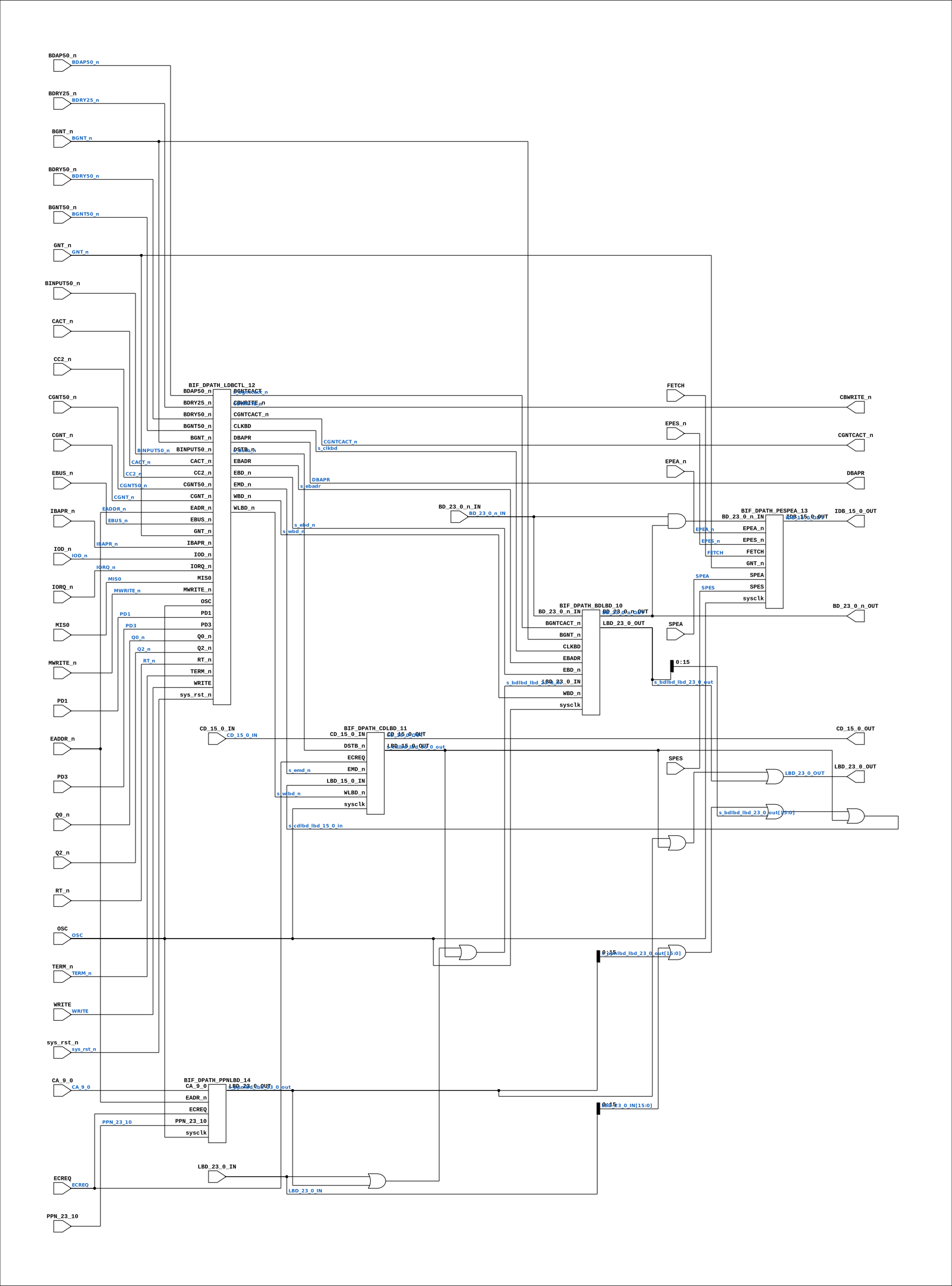
Contains: BIF_DPATH_BDLBD_10, BIF_DPATH_CDLBD_11, BIF_DPATH_LDBCTL_12, BIF_DPATH_PESPEA_13, BIF_DPATH_PPNLBD_14
Module hierarchy - All modules
Schematic
Drawn from the Verilog: the yosys netlist of the Simulation (Verilator) build, instance CORE.CPU_BOARD.BIF.DPATH. Sub-modules are boxes (click the picture to open it full size; there every sub-module box links to its page, and every wire shows its Verilog name).
Description
ND120 CPU, MM&M BIF/DPATH BIF DATA PATH SHEET 9 of 5 0 Last reviewed: 14-DEC-2024 Ronny Hansen
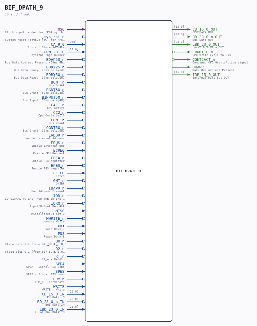
Ports
| Direction | Width | Name | Description |
|---|---|---|---|
| input | 1 |
OSC |
Clock input (added for FPGA synthesis) |
| input | 1 |
sys_rst_n (active low) |
System reset (active low, for FPGA synthesis) |
| input | [9:0] |
CA_9_0 |
Control Store Address |
| input | [13:0] |
PPN_23_10 |
Physical Page Number |
| input | 1 |
BDAP50_n (active low) |
Bus Data Address Present (50ns delayed) |
| input | 1 |
BDRY25_n (active low) |
Bus Data Ready (25ns delayed) |
| input | 1 |
BDRY50_n (active low) |
Bus Data Ready (50ns delayed) |
| input | 1 |
BGNT_n (active low) |
Bus Grant |
| input | 1 |
BGNT50_n (active low) |
Bus Grant (50ns delayed) |
| input | 1 |
BINPUT50_n (active low) |
Bus Input (50ns delayed) |
| input | 1 |
CACT_n (active low) |
CPU Active |
| input | 1 |
CC2_n (active low) |
Cpu Cycle bit 2 |
| input | 1 |
CGNT_n (active low) |
Bus Grant |
| input | 1 |
CGNT50_n (active low) |
Bus Grant (50ns delayed) |
| input | 1 |
EADDR_n (active low) |
Enable External Address |
| input | 1 |
EBUS_n (active low) |
Enable External Bus |
| input | 1 |
ECREQ |
Enable CPU Request |
| input | 1 |
EPEA_n (active low) |
Enable PEA register |
| input | 1 |
EPES_n (active low) |
Enable PES register |
| input | 1 |
FETCH |
Fetch |
| input | 1 |
GNT_n (active low) |
Grant |
| input | 1 |
IBAPR_n (active low) |
Bus Address Present |
| input | 1 |
IOD_n (active low) |
IO SIGNAL TO LAST FOR THE ENTIRE BUS CYCLE |
| input | 1 |
IORQ_n (active low) |
Input/Output Request |
| input | 1 |
MIS0 |
Miscellaneous bit 0 |
| input | 1 |
MWRITE_n (active low) |
Memory Write |
| input | 1 |
PD1 |
Power Down 1 |
| input | 1 |
PD3 |
Power Down 3 |
| input | 1 |
Q0_n (active low) |
State bits 0-2 (from BIF_BCTL_6.Q_2_0_n[0]) |
| input | 1 |
Q2_n (active low) |
State bits 0-2 (from BIF_BCTL_6.Q_2_0_n[2]) |
| input | 1 |
RT_n (active low) |
RT_n - Return |
| input | 1 |
SPEA |
SPEA - Signal PEA Load |
| input | 1 |
SPES |
SPES - Signal PES Load |
| input | 1 |
TERM_n (active low) |
TERM_n - Terminate |
| input | 1 |
WRITE |
WRITE - Write |
| input | [15:0] |
CD_15_0_IN |
CPU Data IN |
| output | [15:0] |
CD_15_0_OUT |
CPU Data OUT |
| input | [23:0] |
BD_23_0_n_IN |
Bus Data IN |
| output | [23:0] |
BD_23_0_n_OUT |
Bus Data OUT |
| input | [23:0] |
LBD_23_0_IN |
Local Bus Data IN |
| output | [23:0] |
LBD_23_0_OUT |
Local Bus Data OUT |
| output | 1 |
CBWRITE_n (active low) |
CPU Write cycle to Bus |
| output | 1 |
CGNTCACT_n (active low) |
Combined CPU Grant/Active signal |
| output | 1 |
DBAPR |
Data Bus Address Present |
| output | [15:0] |
IDB_15_0_OUT |
Internal Data Bus OUT |
Verilog source
Verilog/CPU-BOARD-3202/circuit/BIF_DPATH_9.v on GitHub.
Show the Verilog of BIF_DPATH_9 (326 lines)
/**************************************************************************
   ** ND120 CPU, MM&M                                                       **
   ** BIF/DPATH                                                             **
   ** BIF DATA PATH                                                         **
   ** SHEET 9 of 5 0                                                        **
   **                                                                       **
   ** Last reviewed: 14-DEC-2024                                            **
   ** Ronny Hansen                                                          **
   ***************************************************************************/

module BIF_DPATH_9 (
    // Clock signal
    input OSC,         //! Clock input (added for FPGA synthesis)
    input sys_rst_n,   //! System reset (active low, for FPGA synthesis)

    // Input signals
    input [ 9:0] CA_9_0,    //! Control Store Address
    input [13:0] PPN_23_10, //! Physical Page Number

    input BDAP50_n,    //! Bus Data Address Present (50ns delayed)
    input BDRY25_n,    //! Bus Data Ready (25ns delayed)
    input BDRY50_n,    //! Bus Data Ready (50ns delayed)
    input BGNT_n,      //! Bus Grant
    input BGNT50_n,    //! Bus Grant (50ns delayed)
    input BINPUT50_n,  //! Bus Input (50ns delayed)
    input CACT_n,      //! CPU Active
    input CC2_n,       //! Cpu Cycle bit 2
    input CGNT_n,      //! Bus Grant
    input CGNT50_n,    //! Bus Grant (50ns delayed)
    input EADDR_n,     //! Enable External Address
    input EBUS_n,      //! Enable External Bus
    input ECREQ,       //! Enable CPU Request
    input EPEA_n,      //! Enable PEA register
    input EPES_n,      //! Enable PES register
    input FETCH,       //! Fetch
    input GNT_n,       //! Grant
    input IBAPR_n,     //! Bus Address Present
    input IOD_n,       //! IO SIGNAL TO LAST FOR THE ENTIRE BUS CYCLE
    input IORQ_n,      //! Input/Output Request
    input MIS0,        //! Miscellaneous bit 0
    input MWRITE_n,    //! Memory Write
    input PD1,         //! Power Down 1
    input PD3,         //! Power Down 3
    input Q0_n,        //! State bits 0-2 (from BIF_BCTL_6.Q_2_0_n[0])
    input Q2_n,        //! State bits 0-2 (from BIF_BCTL_6.Q_2_0_n[2])
    input RT_n,        //! RT_n - Return
    input SPEA,        //! SPEA - Signal PEA Load
    input SPES,        //! SPES - Signal PES Load
    input TERM_n,      //! TERM_n - Terminate
    input WRITE,       //! WRITE - Write

    // In-Out signals
    input  [15:0] CD_15_0_IN,  //! CPU Data IN
    output [15:0] CD_15_0_OUT, //! CPU Data OUT

    input  [23:0] BD_23_0_n_IN,  //! Bus Data IN
    output [23:0] BD_23_0_n_OUT, //! Bus Data OUT

    input  [23:0] LBD_23_0_IN,  //! Local Bus Data IN
    output [23:0] LBD_23_0_OUT, //! Local Bus Data OUT

    // Output signals
    output        CBWRITE_n,    //! CPU Write cycle to Bus
    output        CGNTCACT_n,   //! Combined CPU Grant/Active signal
    output        DBAPR,        //! Data Bus Address Present
    output [15:0] IDB_15_0_OUT  //! Internal Data Bus OUT
);

  /*******************************************************************************
      ** The wires are defined here                                                 **
      *******************************************************************************/
  wire        s_osc;

  wire [ 9:0] s_ca_9_0;

  wire [13:0] s_ppn_23_10;

  wire [15:0] s_idb_15_0_out;

  wire [15:0] s_cd_15_0_in;
  wire [15:0] s_cd_15_0_out;

  wire [23:0] s_bd_23_0_n_in;
  wire [23:0] s_bd_23_0_n_out;

  wire [23:0] s_lbd_23_0_out;
  wire [23:0] s_lbd_23_0_in;

  wire [23:0] s_ppnlbd_lbd_23_0_out;

  wire [15:0] s_cdlbd_lbd_15_0_in;
  wire [15:0] s_cdlbd_lbd_15_0_out;

  wire [23:0] s_bdlbd_lbd_23_0_in;
  wire [23:0] s_bdlbd_lbd_23_0_out;

  wire        s_bdap50_n;
  wire        s_bdry25_n;
  wire        s_bdry50_n;
  wire        s_bgnt_n;
  wire        s_bgnt50_n;
  wire        s_bgntcact_n;
  wire        s_binput50_n;
  wire        s_cact_n;
  wire        s_cbwrite_n;
  wire        s_cc2_n;
  wire        s_cgnt_n;
  wire        s_cgnt50_n;
  wire        s_cgntcact_n;
  wire        s_clkbd;
  wire        s_dbapr;
  wire        s_dstb_n;
  wire        s_eaddr_n;
  wire        s_ebadr;
  wire        s_ebd_n;
  wire        s_ebus_n;
  wire        s_ecreq;
  wire        s_emd_n;
  wire        s_epea_n;
  wire        s_epes_n;
  wire        s_fetch;
  wire        s_gnt_n;
  wire        s_ibapr_n;
  wire        s_iod_n;
  wire        s_iorq_n;
  wire        s_mis0;
  wire        s_mwrite_n;
  wire        s_pd1;
  wire        s_pd3;
  wire        s_q0_n;
  wire        s_q2_n;
  wire        s_rt_n;
  wire        s_spea;
  wire        s_spes;
  wire        s_term_n;
  wire        s_wbd_n;
  wire        s_wlbd_n;
  wire        s_write;

  /*******************************************************************************
  ** Here all input connections are defined                                     **
  *******************************************************************************/
  assign s_osc                = OSC;
  assign s_ppn_23_10[13:0]    = PPN_23_10;
  assign s_ca_9_0[9:0]        = CA_9_0;
  assign s_eaddr_n            = EADDR_n;
  assign s_ecreq              = ECREQ;
  assign s_gnt_n              = GNT_n;
  assign s_epes_n             = EPES_n;
  assign s_spea               = SPEA;
  assign s_fetch              = FETCH;
  assign s_spes               = SPES;
  assign s_epea_n             = EPEA_n;
  assign s_bgnt_n             = BGNT_n;
  assign s_write              = WRITE;
  assign s_bdap50_n           = BDAP50_n;
  assign s_cact_n             = CACT_n;
  assign s_bdry25_n           = BDRY25_n;
  assign s_bdry50_n           = BDRY50_n;
  assign s_cgnt_n             = CGNT_n;
  assign s_cgnt50_n           = CGNT50_n;
  assign s_cc2_n              = CC2_n;
  assign s_q0_n               = Q0_n;
  assign s_q2_n               = Q2_n;
  assign s_ebus_n             = EBUS_n;
  assign s_ibapr_n            = IBAPR_n;
  assign s_mwrite_n           = MWRITE_n;
  assign s_pd1                = PD1;
  assign s_iod_n              = IOD_n;
  assign s_binput50_n         = BINPUT50_n;
  assign s_iorq_n             = IORQ_n;
  assign s_term_n             = TERM_n;
  assign s_rt_n               = RT_n;
  assign s_pd3                = PD3;
  assign s_mis0               = MIS0;
  assign s_bgnt50_n           = BGNT50_n;

  assign s_cd_15_0_in[15:0]   = CD_15_0_IN[15:0];
  assign s_bd_23_0_n_in[23:0] = BD_23_0_n_IN[23:0];

  /*******************************************************************************
   ** Here all output connections are defined                                    **
   *******************************************************************************/
  assign CBWRITE_n            = s_cbwrite_n;
  assign CGNTCACT_n           = s_cgntcact_n;
  assign DBAPR                = s_dbapr;

  assign BD_23_0_n_OUT        = s_bd_23_0_n_out[23:0];
  assign CD_15_0_OUT          = s_cd_15_0_out[15:0];
  assign IDB_15_0_OUT         = s_idb_15_0_out[15:0];
  assign LBD_23_0_OUT         = s_lbd_23_0_out[23:0];


  // Or together output signals of the LBD_23_OUT from the different modules.
  assign s_lbd_23_0_in        = LBD_23_0_IN;
  assign s_lbd_23_0_out       = s_ppnlbd_lbd_23_0_out | s_cdlbd_lbd_15_0_out | s_bdlbd_lbd_23_0_out;

  // The CDLBD's LBD pin is ONE bidirectional node on the board: when the chip
  // itself drives LBD (A_OUT, regB->LBD during a CPU write), its own input
  // register samples that same pin. Leaving the chip's own output out of its
  // input made the DSTB_n-rise capture (PALASM 44302B: "DSTB TO SAMPLE DATA AT
  // LBD/CD BUFFERS") read a dead bus during IOX writes, so the end-of-cycle
  // echo (EMD window, WLBD_n high: regA -> CD -> DBR) delivered 0 and the
  // microcode's unconditional A := DBR zeroed the A register on EVERY IOX
  // OUTPUT. No combinational loop: A_OUT depends on regB, never on A_IN.
  assign s_cdlbd_lbd_15_0_in  = s_lbd_23_0_in[15:0] | s_ppnlbd_lbd_23_0_out[15:0] | s_bdlbd_lbd_23_0_out[15:0] | s_cdlbd_lbd_15_0_out[15:0];
  assign s_bdlbd_lbd_23_0_in  = s_lbd_23_0_in[23:0] | s_ppnlbd_lbd_23_0_out[23:0] | s_cdlbd_lbd_15_0_out[15:0];

  /*******************************************************************************
   ** Here all sub-circuits are defined                                          **
   *******************************************************************************/

  BIF_DPATH_PPNLBD_14 PPNLBD (
      // Inputs
      .sysclk(OSC),  // OSC == sysclk (clk_cpu BUFG) on FPGA
      .CA_9_0(s_ca_9_0[9:0]),           // 10-bit address
      .EADR_n(s_eaddr_n),               // Address enable (active low)
      .ECREQ(s_ecreq),                  // Enable CPU Request
      .PPN_23_10(s_ppn_23_10[13:0]),    // Physical Page Number (PPN)

      // Outputs
      .LBD_23_0_OUT(s_ppnlbd_lbd_23_0_out[23:0]) //24-bit  Local Bus Data OUT
  );

  BIF_DPATH_CDLBD_11 CDLBD (
      // Inputs
      .sysclk(OSC),  // OSC == sysclk (clk_cpu BUFG) on FPGA
      .CD_15_0_IN(s_cd_15_0_in[15:0]),
      .DSTB_n(s_dstb_n),
      .ECREQ(s_ecreq),
      .EMD_n(s_emd_n),
      .LBD_15_0_IN(s_cdlbd_lbd_15_0_in[15:0]),
      .WLBD_n(s_wlbd_n),

      // Outputs
      .CD_15_0_OUT (s_cd_15_0_out[15:0]),
      .LBD_15_0_OUT(s_cdlbd_lbd_15_0_out[15:0])
  );

  BIF_DPATH_BDLBD_10 BDLBD (
      // Bus signals
      .sysclk(OSC),  // OSC == sysclk (clk_cpu BUFG) on FPGA
      .BD_23_0_n_IN (s_bd_23_0_n_in[23:0]),
      .BD_23_0_n_OUT(s_bd_23_0_n_out[23:0]),
      .LBD_23_0_IN  (s_bdlbd_lbd_23_0_in[23:0]),
      .LBD_23_0_OUT (s_bdlbd_lbd_23_0_out[23:0]),

      // Inputs
      .BGNTCACT_n(s_bgntcact_n),
      .BGNT_n(s_bgnt_n),
      .CLKBD(s_clkbd),
      .EBADR(s_ebadr),
      .EBD_n(s_ebd_n),

      // Outputs
      .WBD_n(s_wbd_n)
  );

  BIF_DPATH_PESPEA_13 PESPEA (
      // Inputs
      .sysclk(OSC),  // OSC == sysclk (clk_cpu BUFG) on FPGA
      // The PES/PEA capture chips sit on the BIDIRECTIONAL BD net (schematic
      // sheet 13). BD is an active-low wired-AND: the effective net value is
      // the AND of the external input and our own drivers (BDLBD releases to
      // all-ones when EBD_n is inactive). Tapping only the external IN side
      // captured the idle bus (all-ones -> inverted to 0) instead of the
      // address our own BIF was driving - PAGING test 11 read PES/PEA as 0.
      .BD_23_0_n_IN(s_bd_23_0_n_in[23:0] & s_bd_23_0_n_out[23:0]),
      .EPEA_n(s_epea_n),
      .EPES_n(s_epes_n),
      .FETCH(s_fetch),
      .GNT_n(s_gnt_n),

      // Outputs
      .SPEA(s_spea),
      .SPES(s_spes),
      .IDB_15_0_OUT(s_idb_15_0_out[15:0])
  );

  BIF_DPATH_LDBCTL_12 LDBCTL (
      // Clock and reset (added for FPGA synthesis)
      .OSC(s_osc),
      .sys_rst_n(sys_rst_n),

      // Inputs
      .BDAP50_n(s_bdap50_n),
      .BDRY25_n(s_bdry25_n),
      .BDRY50_n(s_bdry50_n),
      .BGNT50_n(s_bgnt50_n),
      .BGNT_n(s_bgnt_n),
      .BINPUT50_n(s_binput50_n),
      .CACT_n(s_cact_n),
      .CC2_n(s_cc2_n),
      .CGNT50_n(s_cgnt50_n),
      .CGNT_n(s_cgnt_n),
      .CLKBD(s_clkbd),
      .EBUS_n(s_ebus_n),
      .GNT_n(s_gnt_n),
      .IBAPR_n(s_ibapr_n),
      .IOD_n(s_iod_n),
      .IORQ_n(s_iorq_n),
      .MIS0(s_mis0),
      .MWRITE_n(s_mwrite_n),
      .PD1(s_pd1),
      .PD3(s_pd3),
      .Q0_n(s_q0_n),
      .Q2_n(s_q2_n),
      .RT_n(s_rt_n),
      .TERM_n(s_term_n),
      .WRITE(s_write),

      // Outputs
      .BGNTCACT(s_bgntcact_n),
      .CBWRITE_n(s_cbwrite_n),
      .CGNTCACT_n(s_cgntcact_n),
      .DBAPR(s_dbapr),
      .DSTB_n(s_dstb_n),
      .EADR_n(s_eaddr_n),
      .EBADR(s_ebadr),
      .EBD_n(s_ebd_n),
      .EMD_n(s_emd_n),
      .WBD_n(s_wbd_n),
      .WLBD_n(s_wlbd_n)
  );

endmodule