CYC_TERM_D
Source: Verilog/CPU-BOARD-3202/circuit/CYC_TERM_D.v
Where it sits (Simulation): ND120_TOP > ND120_CORE > ND3202D > CYC_36 > CYC_TERM_D
- instance path: CORE.CPU_BOARD.CYC.U_TERM_D
Used in: CYC_36 (all tops)
Contains: no other modules.
Module hierarchy - All modules
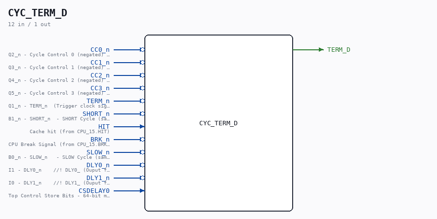
Schematic
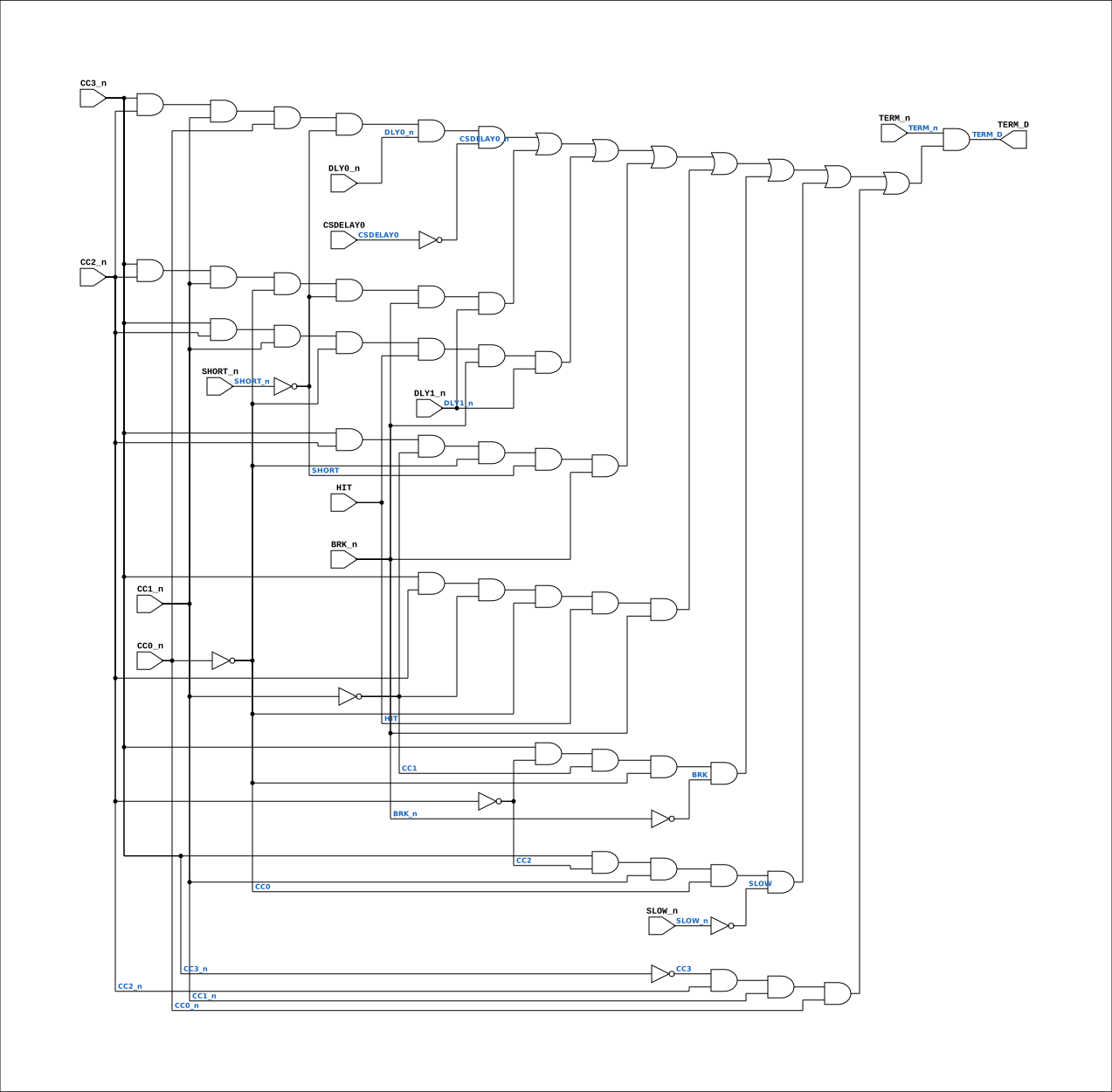
Drawn from the Verilog: the yosys netlist of the Simulation (Verilator) build, instance CORE.CPU_BOARD.CYC.U_TERM_D. Sub-modules are boxes (click the picture to open it full size; there every sub-module box links to its page, and every wire shows its Verilog name).
Description
ND120 CPU, MM&M CYC_TERM_D Combinational NEXT-state of the Cycle Controller TERM register. This is a MIRROR of the TERM_reg next-state logic inside PAL_44601B (the CYCFSM, sheet 36). PAL_44601B stays the golden source; this module reproduces only its TERM D-input so CYC_36 can build a phase-accurate, sysclk-synchronous clock-enable that fires on the SAME edge posedge ALUCLK (~(TERM_n|LCS)) would have, instead of one sysclk late. See docs/clock-enable-refactor.md. DO NOT let this diverge from PAL_44601B. It is validated EXHAUSTIVELY against the real PAL by CYC_TERM_D_tb.v (all 16 CC states x all terminate-input combinations). If PAL_44601B.v changes, re-run that testbench. Last reviewed: 5-JULY-2026 Ronny Hansen
Ports
| Direction | Width | Name | Description |
|---|---|---|---|
| input | 1 |
CC0_n (active low) |
Q2_n - Cycle Control 0 (negated) (from PAL_44601B.CC0_n) |
| input | 1 |
CC1_n (active low) |
Q3_n - Cycle Control 1 (negated) (from PAL_44601B.CC1_n) |
| input | 1 |
CC2_n (active low) |
Q4_n - Cycle Control 2 (negated) (from PAL_44601B.CC2_n) |
| input | 1 |
CC3_n (active low) |
Q5_n - Cycle Control 3 (negated) (from PAL_44601B.CC3_n) |
| input | 1 |
TERM_n (active low) |
Q1_n - TERM_n (Trigger clock signal that latches CS input signals and more) (from PAL_44601B.TERM_n) |
| input | 1 |
SHORT_n (active low) |
B1_n - SHORT_n - SHORT Cycle (same net as PAL_44601B.SHORT_n) |
| input | 1 |
HIT |
Cache hit (from CPU_15.HIT) |
| input | 1 |
BRK_n (active low) |
CPU Break Signal (from CPU_15.BRK_n) |
| input | 1 |
SLOW_n (active low) |
B0_n - SLOW_n - SLOW Cycle (same net as PAL_44601B.SLOW_n) |
| input | 1 |
DLY0_n (active low) |
I1 - DLY0_n //! DLY0_ (Ouput from PAL 44403 DLY0_n (B0) (same net as PAL_44601B.DLY0_n) |
| input | 1 |
DLY1_n (active low) |
I0 - DLY1_n //! DLY1_ (Ouput from PAL 44404 DLY1_n (B3) (same net as PAL_44601B.DLY1_n) |
| input | 1 |
CSDELAY0 |
Top Control Store Bits - 64-bit microcode control signals (from CPU_15.TOPCSB[26]) |
| output | 1 |
TERM_D |
Verilog source
Verilog/CPU-BOARD-3202/circuit/CYC_TERM_D.v on GitHub.
Show the Verilog of CYC_TERM_D (77 lines)
/**************************************************************************
** ND120 CPU, MM&M                                                       **
** CYC_TERM_D                                                            **
** Combinational NEXT-state of the Cycle Controller TERM register.       **
**                                                                       **
** This is a MIRROR of the TERM_reg next-state logic inside PAL_44601B   **
** (the CYCFSM, sheet 36). PAL_44601B stays the golden source; this      **
** module reproduces only its TERM D-input so CYC_36 can build a         **
** phase-accurate, sysclk-synchronous clock-enable that fires on the     **
** SAME edge posedge ALUCLK (~(TERM_n|LCS)) would have, instead of one   **
** sysclk late. See docs/clock-enable-refactor.md.                       **
**                                                                       **
** DO NOT let this diverge from PAL_44601B. It is validated EXHAUSTIVELY **
** against the real PAL by CYC_TERM_D_tb.v (all 16 CC states x all        **
** terminate-input combinations). If PAL_44601B.v changes, re-run that   **
** testbench.                                                            **
**                                                                       **
** Last reviewed: 5-JULY-2026                                            **
** Ronny Hansen                                                          **
***************************************************************************/

module CYC_TERM_D (
    // Current Cycle-Control state + TERM, taken as the PAL's active-low
    // outputs (CCx_n = ~CCx_reg, TERM_n = ~TERM_reg when OE_n=0). These are
    // exactly the nets CYC_36 already has.
    input CC0_n,  //! Q2_n - Cycle Control 0 (negated) (from PAL_44601B.CC0_n)
    input CC1_n,  //! Q3_n - Cycle Control 1 (negated) (from PAL_44601B.CC1_n)
    input CC2_n,  //! Q4_n - Cycle Control 2 (negated) (from PAL_44601B.CC2_n)
    input CC3_n,  //! Q5_n - Cycle Control 3 (negated) (from PAL_44601B.CC3_n)
    input TERM_n,  //! Q1_n - TERM_n  (Trigger clock signal that latches CS input signals and more) (from PAL_44601B.TERM_n)

    // Terminate-condition inputs - the same nets PAL_44601B receives.
    input SHORT_n,  //! B1_n - SHORT_n  - SHORT Cycle (same net as PAL_44601B.SHORT_n)
    input HIT,  //! Cache hit (from CPU_15.HIT)
    input BRK_n,  //! CPU Break Signal (from CPU_15.BRK_n)
    input SLOW_n,  //! B0_n - SLOW_n   - SLOW Cycle (same net as PAL_44601B.SLOW_n)
    input DLY0_n,  //! I1 - DLY0_n    //! DLY0_ (Ouput from PAL 44403 DLY0_n (B0) (same net as PAL_44601B.DLY0_n)
    input DLY1_n,  //! I0 - DLY1_n    //! DLY1_ (Ouput from PAL 44404 DLY1_n (B3) (same net as PAL_44601B.DLY1_n)
    input CSDELAY0,  //! Top Control Store Bits - 64-bit microcode control signals (from CPU_15.TOPCSB[26])

    // Combinational next value of TERM_reg (its D input, before the edge).
    output TERM_D
);

  // Active-high current state bits and the PAL's internal negated wires.
  wire CC0 = ~CC0_n;
  wire CC1 = ~CC1_n;
  wire CC2 = ~CC2_n;
  wire CC3 = ~CC3_n;
  wire s_cc0_n_int = CC0_n;  // = ~CC0_reg
  wire s_cc1_n_int = CC1_n;
  wire s_cc2_n_int = CC2_n;
  wire s_cc3_n_int = CC3_n;
  wire s_term_n_int = TERM_n; // = ~TERM_reg ; TERM_D asserts only when currently deasserted

  // PAL input polarities (match PAL_44601B.v)
  wire SHORT      = ~SHORT_n;
  wire SLOW       = ~SLOW_n;
  wire BRK        = ~BRK_n;
  wire CSDELAY0_n = ~CSDELAY0;

  // ====================================================================
  // MIRROR of PAL_44601B TERM_reg next-state (PAL_44601B.v lines 112-123):
  //   TERM_reg <= s_term_n_int ? (terminate OR-plane) : 1'b0;
  // = s_term_n_int & (OR-plane). Keep term-for-term identical to the PAL.
  // ====================================================================
  assign TERM_D = s_term_n_int & (
        (s_cc3_n_int & s_cc2_n_int & s_cc1_n_int & s_cc0_n_int & SHORT & DLY0_n & CSDELAY0_n)  // 50NS  a
      | (s_cc3_n_int & s_cc2_n_int & s_cc1_n_int & CC0 & SHORT & BRK_n & DLY1_n)               // 75NS  b
      | (s_cc3_n_int & s_cc2_n_int & s_cc1_n_int & CC0 & HIT   & BRK_n & DLY1_n)               // 75NS  b
      | (s_cc3_n_int & s_cc2_n_int & CC1 & CC0 & SHORT & BRK_n)                                // 100NS c
      | (s_cc3_n_int & s_cc2_n_int & CC1 & CC0 & HIT   & BRK_n)                                // 100NS c
      | (s_cc3_n_int & CC2 & CC1 & CC0 & BRK)                                                  // BRK   f
      | (s_cc3_n_int & CC2 & s_cc1_n_int & CC0 & SLOW)                                         // SLOW  g
      | (CC3 & s_cc2_n_int & s_cc1_n_int & s_cc0_n_int) );                                     // p (1000, unconditional)

endmodule