ND3202D
Source: Verilog/CPU-BOARD-3202/circuit/ND3202D.v
Where it sits (Simulation): ND120_TOP > ND120_CORE > ND3202D
- instance path: CORE.CPU_BOARD
Used in: ND120_CORE (all tops)
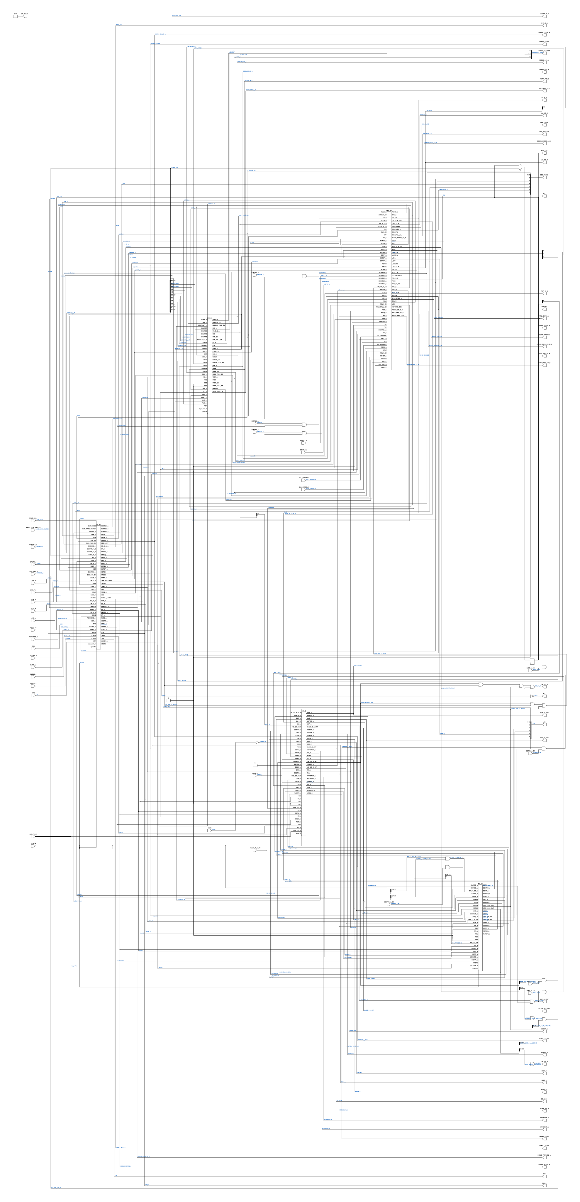
Contains: BIF_5, CPU_15, CYC_36, IO_37, MEM_43
Module hierarchy - All modules
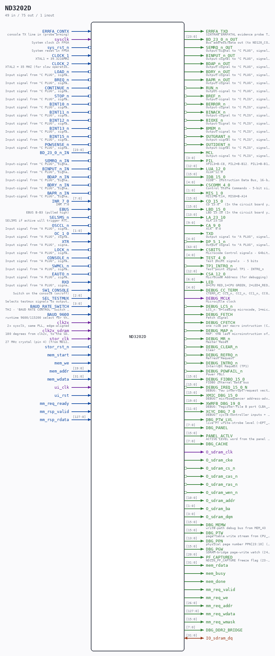
Schematic
Drawn from the Verilog: the yosys netlist of the Simulation (Verilator) build, instance CORE.CPU_BOARD. Sub-modules are boxes (click the picture to open it full size; there every sub-module box links to its page, and every wire shows its Verilog name).
Description
ND120 CPU, MM&M CPU CPU TOP LEVEL SHEET 16 of 50 Last reviewed: 22-MAR-2025 Ronny Hansen
Ports
| Direction | Width | Name | Description |
|---|---|---|---|
| input | 1 |
ERRFA_CONTX |
console TX line in (probe arming) |
| output | 1 |
ERRFA_TXD |
SINTRAN ERRFATAL evidence probe TX (from MEM_43/RAM) |
| input | 1 |
sysclk |
System clock in FPGA |
| input | 1 |
sys_rst_n (active low) |
System reset in FPGA |
| input | 1 |
CLOCK_1 |
XTAL1 = 39.3216MHZ |
| input | 1 |
CLOCK_2 |
XTAL2 = 35 MHZ (for slow operations?) |
| input | 1 |
LOAD_n (active low) |
Input signal from "C PLUG", signal B12 - LOAD_n |
| input | 1 |
BREQ_n (active low) |
Input signal from "C PLUG", signal C12 - BREQ_n (DMA BUS Request) |
| input | 1 |
CONTINUE_n (active low) |
Input signal from "C PLUG", signal B15 - CONTINUE_n |
| input | 1 |
STOP_n (active low) |
Input signal from "C PLUG", signal B16 - STOP_n |
| input | 1 |
BINT10_n (active low) |
Input signal from "C PLUG", signal A15 - BINT10_n |
| input | 1 |
BINT11_n (active low) |
Input signal from "C PLUG", signal C15 - BINT11_n |
| input | 1 |
BINT12_n (active low) |
Input signal from "C PLUG", signal A16 - BINT12_n |
| input | 1 |
BINT13_n (active low) |
Input signal from "C PLUG", signal C16 - BINT13_n |
| input | 1 |
BINT15_n (active low) |
Input signal from "C PLUG", signal C17 - BINT15_n |
| input | 1 |
POWSENSE_n (active low) |
Input signal from "C PLUG", signals A29,B29,C29 - POWSENSE_n (Power sense signal from the PSU?) |
| input | [23:0] |
BD_23_0_n_IN |
|
| output | [23:0] |
BD_23_0_n_OUT |
Bus address/data out (to ND120_CORE.BD_23_0_n_OUT) |
| input | 1 |
SEMRQ_n_IN |
Input-signal from "C PLUG", signal A17 SEMREQ~ (SEMaphore REQest) |
| output | 1 |
SEMRQ_n_OUT |
Output-signal to "C PLUG", signal A17 SEMREQ~ (SEMaphore REQest) |
| input | 1 |
BINPUT_n_IN |
Input-signal from "C PLUG", signal A18 BINPUT~ (Bus INPUT) |
| output | 1 |
BINPUT_n_OUT |
Output-signal to "C PLUG", signal A18 BINPUT~ (Bus INPUT) |
| input | 1 |
BDAP_n_IN |
Input-signal from "C PLUG", signal C18 BDAP~ (Bus DAta Present) |
| output | 1 |
BDAP_n_OUT |
Output-signal to "C PLUG", signal C18 BDAP~ (Bus DAta Present) |
| input | 1 |
BDRY_n_IN |
Input-signal from "C PLUG", signal A19 BDRY~ (Bus Data ReadY) |
| output | 1 |
BDRY_n_OUT |
Output-signal to "C PLUG", signal A19 BDRY~ (Bus Data ReadY) |
| input | 1 |
BAPR_n_IN |
Input-signal from "C PLUG", signal A20 BAPR~ (Bus Address PResent) |
| output | 1 |
BAPR_n_OUT |
Output-signal to "C PLUG", signal A20 BAPR~ (Bus Address PResent) |
| output | 1 |
RUN_n (active low) |
Output-signal to "C PLUG", signal B14 RUN~ (driven by Stop flip-flop: low while CPU is running) |
| output | 1 |
BREF_n (active low) |
Output-signal to "C PLIG", signal B12 BREF~ |
| output | 1 |
BERROR_n (active low) |
Output-signal to "C PLIG", signal B21 BERROR~ |
| output | 1 |
BINACK_n (active low) |
Output-signal to "C PLIG", signal B19 BINACK~ |
| output | 1 |
BIOXE_n (active low) |
Output-signal to "C PLIG", signal C19 BIOXE~ |
| output | 1 |
BMEM_n (active low) |
Output-signal to "C PLIG", signal C28 BMEM~ |
| output | 1 |
OUTGRANT_n (active low) |
Output-signal to "C PLIG", signal C23 OUTGRANT~ (After BREQ request) |
| output | 1 |
OUTIDENT_n (active low) |
Output-signal to "C PLIG", signal C22 OUTIDENT~ |
| output | 1 |
MCL |
Output-signal to "C PLIG", signal B20 MCL~ (after negation) |
| input | [7:0] |
INR_7_0 |
INR 7:0 |
| input | 1 |
EBUS |
EBUS B-B3 (pulled high) |
| input | 1 |
SEL5MS_n (active low) |
SEL5MS if active will trigger RTC after 5 ms, not 20ms) |
| output | [3:0] |
PIL |
XPIL3=B-C8, PIL2=B-B12. PIL1=B-B10, PIL0=B-B9 |
| output | [12:0] |
LUA_12_0 |
XLUA 12:0 |
| output | [15:0] |
IDB_15_0 |
XIDB - Instruction Data Bus, 16-bit bidirectional bus used for transferring instructions and data between CPU components |
| output | [4:0] |
CSCOMM_4_0 |
Control Store Commands - 5-bit signal carrying microcode command bits to control CPU operations |
| output | [1:0] |
MIS_1_0 |
MIS1=B-C14, MIS0=B-A14 |
| output | [15:0] |
CD_15_0 |
CD 15:0 (In the circuit board you strap so that the output to the XIDB15-0 signal is either IDB or LBD) See page 3 in the 3202D schematic) |
| output | [15:0] |
LBD_15_0 |
LBD 15:10 (In the circuit board you strap so that the output to the XIDB15-0 signal is either IDB or LBD) See page 3 in the 3202D schematic) |
| output | [13:0] |
LA_23_10 |
XLA 23:10 |
| output | [9:0] |
CA_9_0 |
XCA 9:0 |
| input | 1 |
OSCCL_n (active low) |
Input signal from "A PLUG", signal B3 - OSCCL_n => (TO IO OSCCL_n) |
| input | [1:0] |
OC_1_0 |
Input signal from "A PLUG", signal C6 (OC0) and A6 (OC1) => (TO IO OC_1_0) |
| input | 1 |
XTR |
Input signal from "A PLUG", signal B4/C23 - XTR => (TO IO XTR) |
| input | 1 |
LOCK_n (active low) |
Input signal from "A PLUG", signal B12 - LOCK_n |
| input | 1 |
CONSOLE_n (active low) |
Input signal from "A PLUG", signal C21/C30 - CONSOLE_n |
| input | 1 |
SWMCL_n (active low) |
Input signal from "A PLUG", signal C16 - SWMCL_n (Switch SW3 on the PCB 3202D might lock this to GND?) |
| input | 1 |
EAUTO_n (active low) |
Input signal from "A PLUG", signal C19 - EAUTO_n |
| input | 1 |
RXD |
Input signal from "A PLUG", signal C8 - RXD (to the UART RXD) |
| input | 1 |
SW1_CONSOLE |
Switch on the console (on/off) |
| input | [2:0] |
SEL_TESTMUX |
Selects testmux signals to output on TEST_4_0 |
| input | [3:0] |
BAUD_RATE_SWITCH |
TH2 - 'BAUD RATE CONTROL' Switch on the PCB to select baudrate |
| input | 1 |
BAUD_9600 |
runtime 9600/115200 select for the SC2661 line (separate from the microcode thumbwheel above) |
| output | 1 |
TXD |
Output signal to "A PLUG", signal A10 (D2N) and C7 (TXD) (from the UART TXD) |
| output | [4:0] |
DP_5_1_n (active low) |
Output signal to "A PLUG", signal DP~5_1 "Display signals" (C25,C26, C27, C28, C29) |
| output | [63:0] |
CSBITS |
Microcode Control signals - 64bit (for debugging) |
| output | [4:0] |
TEST_4_0 |
Test point signals - 5 bits |
| output | 1 |
TP1_INTRQ_n (active low) |
Test point signal TP1 - INTRQ_n |
| output | [12:0] |
CSA_12_0 |
Microcode Address (for debugging) |
| output | [6:0] |
LED |
0=CPU RED,1=CPU GREEN, 2=LED4_RED_PARITY_ERROR, 3=LED_CPU_GRANT_INDICATOR, 4=LED_BUS_GRANT_INDICATOR, 5=LED1 from MMU 6=LED5_RED_DISABLE_PARITY |
| output | [4:0] |
DEBUG_CC_TERM |
{TERM_n, CC3_n, CC2_n, CC1_n, CC0_n} |
| output | 1 |
DEBUG_MCLK |
Microcycle clock |
| output | 1 |
DEBUG_LCS_n (active low) |
LCS_n: 0=loading microcode, 1=microcode loaded |
| output | 1 |
DEBUG_FETCH |
Fetch signal |
| output | 1 |
DEBUG_CFETCH |
one rise per macro instruction (CGA CFETCH via XCFETCH_DBG) - the MIPS event |
| output | 1 |
DEBUG_MAP_n (active low) |
MAP: the last microinstruction of every macro instruction |
| output | 1 |
DEBUG_MR_n (active low) |
Master Reset |
| output | 1 |
DEBUG_CLEAR_n (active low) |
Clear |
| output | 1 |
DEBUG_REFRQ_n (active low) |
Refresh Request |
| output | 1 |
DEBUG_INTRQ_n (active low) |
Interrupt Request (TP1) |
| output | 1 |
DEBUG_POWFAIL_n (active low) |
Power Fail |
| output | [15:0] |
DEBUG_FIDBO_15_0 |
FIDBO internal data bus |
| output | [15:0] |
DEBUG_IREQ_15_0_N (active low) |
DEBUG: raw interrupt-request vector (active low) |
| output | [15:0] |
XMIC_DBG_15_0 |
DEBUG: microsequencer address-advance probe (Tang 06000-hang) |
| output | [19:0] |
XWRFB_DBG_19_0 |
DEBUG: register-file B port {LBA_3_0, B_15_0} - STERR error number |
| output | [11:0] |
XCYC_DBG_7_0 |
DEBUG: cycle-controller inputs + clock enables |
| output | 1 |
DBG_PTW_LVL |
live PT write-strobe level (~EPT_n & ~WMAP_n, 27-AUG overlap probe) |
| output | [7:0] |
DBG_PANEL |
|
| output | [15:0] |
PANEL_ACTLV |
ACTIVE LEVEL word from the panel processor (IO_37/IO_PANCAL_40) |
| output | [7:0] |
DBG_CACHE |
|
| input | 1 |
clk2x |
2x sysclk, same PLL, edge-aligned |
| input | 1 |
clk2x_sdram |
180 degrees from clk2x, to the SDRAM chip |
| output | 1 |
O_sdram_clk |
|
| output | 1 |
O_sdram_cke |
|
| output | 1 |
O_sdram_cs_n (active low) |
|
| output | 1 |
O_sdram_cas_n (active low) |
|
| output | 1 |
O_sdram_ras_n (active low) |
|
| output | 1 |
O_sdram_wen_n (active low) |
|
| inout | [31:0] |
IO_sdram_dq |
|
| output | [10:0] |
O_sdram_addr |
|
| output | [1:0] |
O_sdram_ba |
|
| output | [3:0] |
O_sdram_dqm |
|
| output | [15:0] |
DBG_MEMW |
write-path debug bus from MEM_43 |
| output | [15:0] |
DBG_PTW |
page-table write stream from CPU_MMU_24 (23-AUG, zero-read campaign) |
| output | [13:0] |
DBG_PPN |
physical page number PPN[23:10] (24-AUG, zero-fetch campaign) |
| output | [15:0] |
DBG_PGW |
SDRAM-bridge page-write watch (24-AUG, zero-page campaign) |
| output | [20:0] |
PF_CAPTURED |
ND120_PF_CAPTURE freeze flag (23-AUG) |
| input | 1 |
stor_clk |
27 MHz crystal (pin 4) (from ND120_TANG20K_TOP.sys_clk) |
| input | 1 |
stor_rst_n (active low) |
|
| input | 1 |
mem_start |
|
| input | 1 |
mem_we |
|
| input | [19:0] |
mem_addr |
|
| input | [31:0] |
mem_wdata |
|
| output | [31:0] |
mem_rdata |
|
| output | 1 |
mem_busy |
|
| output | 1 |
mem_done |
|
| input | 1 |
ui_clk |
|
| input | 1 |
ui_rst |
|
| output | 1 |
mm_req_valid |
|
| output | 1 |
mm_req_we |
|
| output | [26:0] |
mm_req_addr |
|
| output | [127:0] |
mm_req_wdata |
|
| output | [15:0] |
mm_req_wmask |
|
| input | 1 |
mm_req_ready |
|
| input | 1 |
mm_rsp_valid |
|
| input | [127:0] |
mm_rsp_rdata |
|
| output | [7:0] |
DBG_DDR2_BRIDGE |
Verilog source
Verilog/CPU-BOARD-3202/circuit/ND3202D.v on GitHub.
Show the Verilog of ND3202D (1310 lines)
/**************************************************************************
** ND120 CPU, MM&M **
** CPU **
** CPU TOP LEVEL **
** SHEET 16 of 50 **
** **
** Last reviewed: 22-MAR-2025 **
** Ronny Hansen **
***************************************************************************/
// Onboard 4MB RAM (controlled by PAL 44446B)
module ND3202D (
`ifdef ND120_ERRFA_PROBE
input ERRFA_CONTX, // console TX line in (probe arming)
output ERRFA_TXD, // SINTRAN ERRFATAL evidence probe TX (from MEM_43/RAM)
`endif
input sysclk, //! System clock in FPGA
input sys_rst_n, //! System reset in FPGA
/***************************************************
** CLOCK SIGNALS *
***************************************************/
input CLOCK_1, //! XTAL1 = 39.3216MHZ
input CLOCK_2, //! XTAL2 = 35 MHZ (for slow operations?)
/***************************************************
* BACKPLANE C-PLUG *
***************************************************/
/* FROM C-PLUG */
input LOAD_n, //! Input signal from "C PLUG", signal B12 - LOAD_n
input BREQ_n, //! Input signal from "C PLUG", signal C12 - BREQ_n (DMA BUS Request)
// C-PLUG B13 - /RESTART: pulled high on the panel side, NOT CONNECTED to any logic on this board
input CONTINUE_n, //! Input signal from "C PLUG", signal B15 - CONTINUE_n
input STOP_n, //! Input signal from "C PLUG", signal B16 - STOP_n
input BINT10_n, //! Input signal from "C PLUG", signal A15 - BINT10_n
input BINT11_n, //! Input signal from "C PLUG", signal C15 - BINT11_n
input BINT12_n, //! Input signal from "C PLUG", signal A16 - BINT12_n
input BINT13_n, //! Input signal from "C PLUG", signal C16 - BINT13_n
input BINT15_n, //! Input signal from "C PLUG", signal C17 - BINT15_n
input POWSENSE_n, //! Input signal from "C PLUG", signals A29,B29,C29 - POWSENSE_n (Power sense signal from the PSU?)
/* BUS BD to and from C-PLUG - Bidirectional Address and Data*/
input [23:0] BD_23_0_n_IN,
output [23:0] BD_23_0_n_OUT, //! Bus address/data out (to ND120_CORE.BD_23_0_n_OUT)
/* Bidirectional signals */
input SEMRQ_n_IN, //! Input-signal from "C PLUG", signal A17 SEMREQ~ (SEMaphore REQest)
output SEMRQ_n_OUT, //! Output-signal to "C PLUG", signal A17 SEMREQ~ (SEMaphore REQest)
input BINPUT_n_IN, //! Input-signal from "C PLUG", signal A18 BINPUT~ (Bus INPUT)
output BINPUT_n_OUT, //! Output-signal to "C PLUG", signal A18 BINPUT~ (Bus INPUT)
input BDAP_n_IN, //! Input-signal from "C PLUG", signal C18 BDAP~ (Bus DAta Present)
output BDAP_n_OUT, //! Output-signal to "C PLUG", signal C18 BDAP~ (Bus DAta Present)
input BDRY_n_IN, //! Input-signal from "C PLUG", signal A19 BDRY~ (Bus Data ReadY)
output BDRY_n_OUT, //! Output-signal to "C PLUG", signal A19 BDRY~ (Bus Data ReadY)
input BAPR_n_IN, //! Input-signal from "C PLUG", signal A20 BAPR~ (Bus Address PResent)
output BAPR_n_OUT, //! Output-signal to "C PLUG", signal A20 BAPR~ (Bus Address PResent)
/* TO C-PLUG */
output RUN_n, //! Output-signal to "C PLUG", signal B14 RUN~ (driven by Stop flip-flop: low while CPU is running)
output BREF_n, //! Output-signal to "C PLIG", signal B12 BREF~
output BERROR_n, //! Output-signal to "C PLIG", signal B21 BERROR~
output BINACK_n, //! Output-signal to "C PLIG", signal B19 BINACK~
output BIOXE_n, //! Output-signal to "C PLIG", signal C19 BIOXE~
output BMEM_n, //! Output-signal to "C PLIG", signal C28 BMEM~
output OUTGRANT_n, //! Output-signal to "C PLIG", signal C23 OUTGRANT~ (After BREQ request)
output OUTIDENT_n, //! Output-signal to "C PLIG", signal C22 OUTIDENT~
output MCL, //! Output-signal to "C PLIG", signal B20 MCL~ (after negation)
/***************************************************
* BACKPLANE B-PLUG *
***************************************************/
/* FROM B plug */
input [7:0] INR_7_0, //! INR 7:0
input EBUS, //! EBUS B-B3 (pulled high)
input SEL5MS_n, //! SEL5MS if active will trigger RTC after 5 ms, not 20ms)
/* TO B-PLUG */
output [3:0] PIL, // XPIL3=B-C8, PIL2=B-B12. PIL1=B-B10, PIL0=B-B9
output [12:0] LUA_12_0, // XLUA 12:0
output [15:0] IDB_15_0, // XIDB - Instruction Data Bus, 16-bit bidirectional bus used for transferring instructions and data between CPU components
output [4:0] CSCOMM_4_0, // Control Store Commands - 5-bit signal carrying microcode command bits to control CPU operations
output [1:0] MIS_1_0, // MIS1=B-C14, MIS0=B-A14
output [15:0] CD_15_0, // CD 15:0 (In the circuit board you strap so that the output to the XIDB15-0 signal is either IDB or LBD) See page 3 in the 3202D schematic)
output [15:0] LBD_15_0, // LBD 15:10 (In the circuit board you strap so that the output to the XIDB15-0 signal is either IDB or LBD) See page 3 in the 3202D schematic)
output [13:0] LA_23_10, // XLA 23:10
output [9:0] CA_9_0, // XCA 9:0
/***************************************************
* BACKPLANE C-PLUG *
***************************************************/
/* FROM A-PLUG */
input OSCCL_n, // Input signal from "A PLUG", signal B3 - OSCCL_n => (TO IO OSCCL_n)
input [1:0] OC_1_0, // Input signal from "A PLUG", signal C6 (OC0) and A6 (OC1) => (TO IO OC_1_0)
input XTR, // Input signal from "A PLUG", signal B4/C23 - XTR => (TO IO XTR)
input LOCK_n, // Input signal from "A PLUG", signal B12 - LOCK_n
input CONSOLE_n, // Input signal from "A PLUG", signal C21/C30 - CONSOLE_n
input SWMCL_n, // Input signal from "A PLUG", signal C16 - SWMCL_n (Switch SW3 on the PCB 3202D might lock this to GND?)
input EAUTO_n, // Input signal from "A PLUG", signal C19 - EAUTO_n
input RXD, // Input signal from "A PLUG", signal C8 - RXD (to the UART RXD)
// Some other signals from A-PLUG to consider ?
// LOAD_n => SWLD_n
//
/***************************************************
* CONFIGURATION SWITCHES *
***************************************************/
input SW1_CONSOLE, // Switch on the console (on/off)
input [2:0] SEL_TESTMUX, // Selects testmux signals to output on TEST_4_0
input [3:0] BAUD_RATE_SWITCH, // TH2 - 'BAUD RATE CONTROL' Switch on the PCB to select baudrate
input BAUD_9600, // runtime 9600/115200 select for the SC2661 line (separate from the microcode thumbwheel above)
/*******************************************************************************
** The outputs are defined here **
*******************************************************************************/
output TXD, // Output signal to "A PLUG", signal A10 (D2N) and C7 (TXD) (from the UART TXD)
output [4:0] DP_5_1_n, // Output signal to "A PLUG", signal DP~5_1 "Display signals" (C25,C26, C27, C28, C29)
output [63:0] CSBITS, //! Microcode Control signals - 64bit (for debugging)
output [4:0] TEST_4_0, //! Test point signals - 5 bits
output TP1_INTRQ_n, //! Test point signal TP1 - INTRQ_n
output [12:0] CSA_12_0, //! Microcode Address (for debugging)
// Led signals
output [6:0] LED, // 0=CPU RED,1=CPU GREEN, 2=LED4_RED_PARITY_ERROR, 3=LED_CPU_GRANT_INDICATOR, 4=LED_BUS_GRANT_INDICATOR, 5=LED1 from MMU 6=LED5_RED_DISABLE_PARITY
// Debug outputs for FPGA
output [4:0] DEBUG_CC_TERM, // {TERM_n, CC3_n, CC2_n, CC1_n, CC0_n}
output DEBUG_MCLK, // Microcycle clock
output DEBUG_LCS_n, // LCS_n: 0=loading microcode, 1=microcode loaded
// Additional debug outputs for microcode load/boot analysis
output DEBUG_FETCH, // Fetch signal
output DEBUG_CFETCH, // one rise per macro instruction (CGA CFETCH via XCFETCH_DBG) - the MIPS event
output DEBUG_MAP_n, // MAP: the last microinstruction of every macro instruction
// loads the next micro-address from the DGA's opcode mapper.
// One falling edge = one macro instruction dispatched, cache
// hit or miss - unlike FETCH, which marks memory CYCLES and
// goes quiet when the cache serves the fetch (the panel MIPS
// read 00.00 on build 8 for exactly that reason, 30-AUG-2026).
output DEBUG_MR_n, // Master Reset
output DEBUG_CLEAR_n, // Clear
output DEBUG_REFRQ_n, // Refresh Request
output DEBUG_INTRQ_n, // Interrupt Request (TP1)
output DEBUG_POWFAIL_n, // Power Fail
output [15:0] DEBUG_FIDBO_15_0, // FIDBO internal data bus
output [15:0] DEBUG_IREQ_15_0_N, // DEBUG: raw interrupt-request vector (active low)
output [15:0] XMIC_DBG_15_0, // DEBUG: microsequencer address-advance probe (Tang 06000-hang)
output [19:0] XWRFB_DBG_19_0, // DEBUG: register-file B port {LBA_3_0, B_15_0} - STERR error number
output [11:0] XCYC_DBG_7_0, // DEBUG: cycle-controller inputs + clock enables
output DBG_PTW_LVL, // live PT write-strobe level (~EPT_n & ~WMAP_n, 27-AUG overlap probe)
// Operator-panel status, packed in the SAME BIT ORDER as the MC68705U3's
// Port D on the real board (schematic sheet 40 of 50, 5-OCT-1987; see
// IO_PANCAL_40.v). Every one of these already feeds the panel processor
// instance below - this port only brings the same five signals out to the
// FPGA top so a screen can draw what the real panel drew:
//
// [1:0] PCR_1_0 protect ring [4] HIT cache hit (the ND-120's OWN
// [2] PONI paging on cache, not the FPGA line cache)
// [3] IONI interrupt on [5] LEV0 running at level 0 = idle
//
// Bits [7:6] read zero. Purely an observation port: nothing here changes
// what the CPU does, and leaving it unconnected costs nothing.
output [7:0] DBG_PANEL,
output [15:0] PANEL_ACTLV, //! ACTIVE LEVEL word from the panel processor (IO_37/IO_PANCAL_40)
//! DEBUG: cache-write gating bus from CPU_15/CPU_MMU_24. Bit layout and
//! the reason it exists are in CPU_MMU_24.v's DBG_CACHE port comment.
//! Declared unconditionally and at module scope on purpose - two builds
//! have already been lost to a debug wire that lived inside an `ifdef`
//! some configurations do not define.
output [7:0] DBG_CACHE
`ifdef MAIN_RAM_SDRAM
// SDRAM main-memory backend (Tang Nano 20K) - threaded down to MEM_43.
// Absent in Verilator/Basys3 builds.
,
input clk2x, //! 2x sysclk, same PLL, edge-aligned
input clk2x_sdram, //! 180 degrees from clk2x, to the SDRAM chip
output O_sdram_clk,
output O_sdram_cke,
output O_sdram_cs_n,
output O_sdram_cas_n,
output O_sdram_ras_n,
output O_sdram_wen_n,
inout [31:0] IO_sdram_dq,
output [10:0] O_sdram_addr,
output [ 1:0] O_sdram_ba,
output [ 3:0] O_sdram_dqm,
output [15:0] DBG_MEMW, // write-path debug bus from MEM_43
output [15:0] DBG_PTW, // page-table write stream from CPU_MMU_24 (23-AUG, zero-read campaign)
output [13:0] DBG_PPN, // physical page number PPN[23:10] (24-AUG, zero-fetch campaign)
output [15:0] DBG_PGW, // SDRAM-bridge page-write watch (24-AUG, zero-page campaign)
output [20:0] PF_CAPTURED // ND120_PF_CAPTURE freeze flag (23-AUG)
`ifdef ND_STORAGE_PORT
// nd_storage device port - straight through to MEM_43/MEM_RAM_49_SDRAM.
// stor_clk is its own domain (the backend toggle-CDCs it into clk2x).
,
input wire stor_clk, //! 27 MHz crystal (pin 4) (from ND120_TANG20K_TOP.sys_clk)
input wire stor_rst_n,
input wire mem_start,
input wire mem_we,
input wire [19:0] mem_addr,
input wire [31:0] mem_wdata,
output wire [31:0] mem_rdata,
output wire mem_busy,
output wire mem_done
`endif
`endif
`ifdef MAIN_RAM_DDR2
// DDR2 main-memory backend (Nexys 4 DDR) - threaded down to MEM_43.
// ui_clk is the MIG user clock; the client port reaches nd_ddr2_arb at
// the board top. Absent in every other build.
,
input wire ui_clk,
input wire ui_rst,
output wire mm_req_valid,
output wire mm_req_we,
output wire [ 26:0] mm_req_addr,
output wire [127:0] mm_req_wdata,
output wire [ 15:0] mm_req_wmask,
input wire mm_req_ready,
input wire mm_rsp_valid,
input wire [127:0] mm_rsp_rdata,
output wire [ 7:0] DBG_DDR2_BRIDGE
`endif
);
/*
http://norsk-data.com/hardware/nd-100/nd-350002.html
LED1 (red) - Cache disabled
LED2 (red) - Selftest failed
LED3 (green) - Selftest passed
LED4 (red) - Parity error detected
LED5 (red) - Parity error disabled
LED6 (green) - CPU grant
LED7 (yellow) - Bus grant
TODO: Sort bits on output LED to match led numbering
*/
/*******************************************************************************
** The wires are defined here **
*******************************************************************************/
wire [ 1:0] s_csalum_1_0;
wire [ 1:0] s_csdelay_1_0;
wire [ 1:0] s_csmis_1_0;
wire [ 1:0] s_mis_1_0; //Clocked MIS signal PDF page 3, A7 (on raising CLK signal)
wire [ 1:0] s_oc_1_0;
wire [ 1:0] s_pcr_1_0;
wire [ 2:0] s_cc_3_1_n;
wire s_cc0_n;
// Debug output: {TERM_n, CC3_n, CC2_n, CC1_n, CC0_n}
assign DEBUG_CC_TERM = {s_term_n, s_cc_3_1_n[2:0], s_cc0_n};
assign DEBUG_MCLK = s_mclk;
assign DEBUG_LCS_n = s_lcs_n;
assign DEBUG_FETCH = s_fetch;
assign DEBUG_MAP_n = s_map_n;
assign DEBUG_CFETCH = s_cfetch_dbg;
assign DEBUG_MR_n = s_mr_n;
assign DEBUG_CLEAR_n = s_clear_n;
assign DEBUG_REFRQ_n = s_refrq_n;
assign DEBUG_INTRQ_n = s_rp1_intrq_n;
assign DEBUG_POWFAIL_n = s_powfail_n;
wire [ 3:0] s_lba_3_0;
wire [ 3:0] s_pil_3_0;
wire [ 4:0] s_ram_bd_23_19_n;
wire [ 4:0] s_cscomm_4_0;
wire [ 4:0] s_csidbs_4_0;
wire [ 4:0] s_dp_5_1_n;
`ifndef MAIN_RAM_SDRAM
// DBG_PPN / DBG_PTW / PF_CAPTURED are output ports only in the
// MAIN_RAM_SDRAM section of the port list, but the assign below and the
// CPU instance connections use them unconditionally. Without these
// fallbacks the non-SDRAM builds (Verilator, DDR2) create IMPLICIT 1-bit
// nets - which Verilator -Wall treats as a hard error (found 30-AUG-2026
// when runSim stopped verilating). Same rule as the DBG_CACHE port
// comment: a debug wire touched outside a conditional must exist in
// every build.
wire [13:0] DBG_PPN;
wire [15:0] DBG_PTW;
wire [20:0] PF_CAPTURED;
`endif
wire [13:0] s_ppn_23_10;
// 24-AUG: the physical page number the MMU presents, out to the board for
// the zero-fetch probe. PPN20 = [10] and PPN21 = [11] are the two bits the
// bank decode uses (PAL_44445B.v:65-67), and on the Tang BANK1 is NOT
// POPULATED (MEM_RAM_49_SDRAM.v:18 - "never written, reads as 0").
assign DBG_PPN = s_ppn_23_10;
wire [ 4:0] s_test_4_0;
wire [ 7:0] s_inr_7_0; //! INR signals from CONNECTOR B.
wire [ 8:0] s_csalui_8_0;
wire [ 9:0] s_ca_9_0;
wire [12:0] s_lua_12_0;
// CD BUS
wire [15:0] s_bif_cd_15_0_in;
wire [15:0] s_bif_cd_15_0_out;
wire [15:0] s_cpu_cd_15_0_out;
wire [15:0] s_cpu_cd_15_0_in;
// IDB bus
wire [15:0] s_bif_idb_15_0_out;
wire [15:0] s_cpu_idb_15_0_in;
wire [15:0] s_cpu_idb_15_0_out;
wire [ 7:0] s_io_idb_7_0_in;
wire [15:0] s_io_idb_15_0_out;
wire [15:0] s_mem_idb_15_0_out;
// LBD BUS
wire [23:0] s_mem_lbd_23_0_in;
wire [23:0] s_mem_lbd_23_0_out;
wire [23:0] s_bif_lbd_23_0_in;
wire [23:0] s_bif_lbd_23_0_out;
// BD ?
wire [23:0] s_bif_bd_23_0_n_in;
wire [23:0] s_bif_bd_23_0_n_out;
// CSBITS
wire [63:0] s_csbits;
// Wires!
wire s_acond_n; // Output from CGA_MIC_CONDREG. CGA.XACONDN
wire s_aluclk;
// P2 clock-enable pulses from CYC_36 (consumed as domains convert)
/* verilator lint_off UNUSEDSIGNAL */
wire s_cyc_maclk_en;
wire s_cyc_clk_fall_en;
wire s_cyc_uclk_fall_en;
wire s_cyc_maclk_fall_en;
wire s_cyc_aluclk_fall_en;
/* verilator lint_on UNUSEDSIGNAL */
wire s_cyc_clk_en;
wire s_cyc_uclk_en;
wire s_cyc_mclk_en;
wire s_cyc_mclk_fall_en;
wire s_cyc_aluclk_en;
wire s_bapr_n_in;
wire s_bapr_n_out;
wire s_bdap_n_in;
wire s_bdap_n_out;
wire s_bdap50_n;
wire s_bdry_n_in;
wire s_bdry_n_out;
wire s_bdry50_n;
wire s_bgnt_n;
wire s_bgnt50_n;
wire s_bif_bdry_n; // BDRY signal out from BIF module
wire s_binput_n_in;
wire s_binput_n_out;
wire s_bint10_n;
wire s_bint11_n;
wire s_bint12_n;
wire s_bint13_n;
wire s_bint15_n;
wire s_breq_n;
wire s_brk_n;
wire s_ca10;
wire s_cc2_n;
wire s_cclr_n;
wire s_cgnt_n;
wire s_cgnt50_n;
wire s_cgntcact_n;
wire s_clear_n;
wire s_clk;
wire s_console_n;
wire s_continue_n;
wire s_crq_n;
wire s_cx_n;
wire s_cyd;
wire s_dap_n;
wire s_dbapr;
wire s_dt_n;
wire s_dvacc_n; // DGA access qualifier: IO_37 drives it, CPU_15/CPU_MMU_24 consume it. Not the CGA's VACC (CGA_DCD.v).
wire s_eauto_n;
wire s_ebus_n;
wire s_eccr;
wire s_ecreq;
wire s_ecsr_n;
wire s_edo_n;
wire s_emcl_n;
wire s_empid_n;
wire s_eorf_n;
wire s_estof_n;
wire s_etrap_n;
wire s_fetch;
wire s_fmiss;
wire s_form_n;
wire s_gnt_n;
wire s_gnt50_n;
wire s_hit;
wire s_dbg_lapa_n;
//! LHIT from IO_37 - the panel's own cache-hit signal. Declared HERE, at
//! module scope and unconditionally. Two builds have already been lost to a
//! debug wire declared inside an `ifdef` that some configurations do not
//! define (b958fcc, and again during the panel work).
wire s_lhit;
wire s_ibapr_n;
wire s_ibdap_n;
wire s_ibdry_n;
wire s_ibinput_n;
wire s_ibint10_n;
wire s_ibint11_n;
wire s_ibint12_n;
wire s_ibint13_n;
wire s_ibint15_n;
wire s_ibperr_n;
wire s_ibreq_n;
wire s_icontin_n;
wire s_iload_n;
wire s_io_bint10_n;
wire s_io_bint12_n;
wire s_io_bint13_n;
wire s_ioni;
wire s_iorq_n;
wire s_ioxerr_n;
wire s_isemrq_n;
wire s_istop_n;
wire s_lcs_n;
wire s_lerr_n;
wire s_lev0;
wire s_load_n;
wire s_lock_n;
wire s_lperr_n;
wire s_lshadow;
wire s_maclk /* verilator public_flat_rd */; // kept observable for the sim trace harness
wire s_map_n;
wire s_cfetch_dbg; // CGA CFETCH out of CPU_15 (XCFETCH_DBG)
wire s_mclk;
wire s_mem_bdry_n; // BDRY signal out from MEM module
wire s_moff_n;
wire s_mor_n;
wire s_mor25_n;
wire s_mr_n;
wire s_mreq_n;
wire s_mwrite_n;
wire s_opclcs;
wire s_osc;
wire s_osccl_n;
wire s_pa_n;
wire s_pan_n;
wire s_parerr_n;
wire s_pd1;
wire s_pd2;
wire s_pd3;
wire s_pd4;
wire s_poni;
wire s_powfail_n;
wire s_powsense_n;
wire s_ps_n;
wire s_ref_n;
wire s_refrq_n;
wire s_rerr_n;
wire s_rp1_intrq_n;
wire s_rrf_n;
wire s_rt_n;
wire s_run_n;
wire s_rwcs_n;
wire s_rxd;
wire s_sel5ms_n;
wire s_semrq_n_in;
wire s_semrq_n_out;
wire s_semrq50_n;
wire s_short_n;
wire s_slow_n;
wire s_ssema_n;
wire s_stoc_n;
wire s_stop_n;
wire s_stp;
wire s_sw1_console;
wire s_swmcl_n;
wire s_term_n;
wire s_tout;
wire s_trap_n;
wire s_txd;
wire s_uclk;
wire s_vex;
wire s_wchim_n;
wire s_wrfstb;
wire s_write;
wire s_xtal1;
wire s_xtal2;
wire s_xtr;
// Code to make LINTER not complaing about bits _not_ read in s_LDEXM_n
// TODO-CLEANUP: Signal not connected and should probably be refactored away
(* keep = "true", DONT_TOUCH = "true" *) wire s_LDEXM_n;
/*******************************************************************************
** Here all wiring is defined **
*******************************************************************************/
assign s_cscomm_4_0[4:0] = s_csbits[36:32];
assign s_csmis_1_0[1:0] = s_csbits[43:42];
assign s_csalui_8_0[8:0] = s_csbits[63:55];
assign s_csalum_1_0[1:0] = s_csbits[45:44];
assign s_csidbs_4_0[4:0] = s_csbits[41:37];
assign s_csdelay_1_0[1:0] = s_csbits[27:26];
/*******************************************************************************
** Here all input connections are defined **
*******************************************************************************/
// Apply De Morgan's law: ~(!A | !B) => A & B
assign s_bint10_n =(BINT10_n & s_io_bint10_n); // or together with signals from IO interface (IOC chip output) (but must first be negated to get the correct meaning) output PDF page 41
assign s_bint11_n = BINT11_n;
assign s_bint12_n = (BINT12_n & s_io_bint12_n);
assign s_bint13_n = (BINT13_n & s_io_bint13_n);
assign s_bint15_n = BINT15_n;
assign s_breq_n = BREQ_n;
assign s_console_n = CONSOLE_n;
assign s_continue_n = CONTINUE_n;
assign s_eauto_n = EAUTO_n;
assign s_load_n = LOAD_n;
assign s_lock_n = LOCK_n;
assign s_oc_1_0 = OC_1_0;
assign s_osccl_n = OSCCL_n;
assign s_rxd = RXD;
assign s_stop_n = STOP_n;
assign s_sw1_console = SW1_CONSOLE;
assign s_swmcl_n = SWMCL_n;
assign s_xtal1 = CLOCK_1;
assign s_xtal2 = CLOCK_2;
assign s_xtr = XTR;
assign s_bdap_n_in = BDAP_n_IN;
assign s_bdry_n_in = BDRY_n_IN;
assign s_bapr_n_in = BAPR_n_IN;
assign s_binput_n_in = BINPUT_n_IN;
assign s_semrq_n_in = SEMRQ_n_IN;
/*******************************************************************************
** Here all output connections are defined **
*******************************************************************************/
assign CSBITS = s_csbits[63:0];
assign DP_5_1_n = s_dp_5_1_n[4:0];
assign RUN_n = s_run_n;
assign TEST_4_0 = s_test_4_0[4:0];
assign TP1_INTRQ_n = s_rp1_intrq_n;
assign TXD = s_txd;
/*******************************************************************************
** Here all in-lined components are defined **
*******************************************************************************/
// CD BUS connections
assign s_bif_cd_15_0_in = s_cpu_cd_15_0_out;
assign s_cpu_cd_15_0_in = s_bif_cd_15_0_out;
// IDB BUS connections
assign s_cpu_idb_15_0_in = s_bif_idb_15_0_out | s_io_idb_15_0_out | s_mem_idb_15_0_out;
assign s_io_idb_7_0_in = s_bif_idb_15_0_out[7:0] | s_cpu_idb_15_0_out[7:0] | s_mem_idb_15_0_out[7:0];
// LBD BUS connections
assign s_mem_lbd_23_0_in[23:0] = s_bif_lbd_23_0_out[23:0];
assign s_bif_lbd_23_0_in[23:0] = s_mem_lbd_23_0_out[23:0];
// Bif BD_23_0 comes from BIF_DPATH_9
// BD & LBD in and out of BIF
// FIX 24-AUG-2026 - the memory bank was decoded from the WRONG SIDE of the
// bus transceiver, so every DMA write landed in BANK0.
//
// This took the bank-decode bits from s_bif_bd_23_0_n_OUT, which is what
// THIS BOARD DRIVES onto the bus. On a DMA write the board is the SLAVE and
// drives nothing, and BIF_DPATH_BDLBD_10.v:76 idles that output at ~24'b0 -
// all ones, i.e. active-low idle. BD23..BD19 therefore read as 0 on every
// incoming transfer, PAL_44446B.v:66 gives BANK0_n = BD21|BD20 = 0, and the
// write went to BANK0 whatever address the master presented. The row and
// column were unaffected because they come from LBD_19_0, which IS captured
// from the bus INPUT through the TTL_74648 transceivers - so the data landed
// at the right ROW in the wrong BANK.
//
// Measured on Tang silicon 24-AUG-2026: SINTRAN's segment load wrote
// physical page 1016 = {BANK0, row 1016} while the MMU resolved the same
// logical page to 2040 = {BANK2, row 1016}. The CPU then fetched zeros,
// executed them as STZ, ran off into data and died in ERRFATAL. The proof
// was the content: the oracle's words at 064540..064547
// (021114 146145 146131 170017 135111 135111 124064 175035) were found in
// the writes to page 1016.
//
// BD is a shared, active-low bus node: any driver may pull a line low and it
// idles high. The faithful model is therefore the wired-AND of both sides,
// which also stays correct when THIS board is the bus master and drives the
// address itself.
assign s_ram_bd_23_19_n[4:0] = s_bif_bd_23_0_n_in[23:19]
& s_bif_bd_23_0_n_out[23:19]; // for address decoding
// Buffer
assign s_run_n = s_stp;
// PD1-PD4 (Power down) are always 0 during normal function
assign s_pd1 = 0;
assign s_pd2 = 0;
assign s_pd3 = 0;
assign s_pd4 = 0;
// Or together the BIF and MEM bdry signals. Since they are negated we must first negate them to get the correct meaning
// assign s_bdry_n_out = ~(~s_bif_bdry_n | ~s_mem_bdry_n);
// But we can simplify using De Morgan's law: ~(~A | ~B) => A & B
assign s_bdry_n_out = (s_bif_bdry_n & s_mem_bdry_n);
// Combined IO signals input to chip 5C
// (if one (or both) of IN or OUT is low, that means the combined signal is low)
// Cpu Cycle Clock
assign s_cc2_n = s_cc_3_1_n[1];
// ********************************************
// **** Bus B connector (TRACE BUS) ****
// ********************************************
assign s_ebus_n = ~EBUS;
assign s_sel5ms_n = SEL5MS_n; // B14 (SEL5MS~) Pulled high via 1Kohm. (3202D pdf sheet 3) - Select 5ms (if active will trigger RTC after 5 ms, not 20ms)
assign s_inr_7_0 = INR_7_0;
assign PIL = s_pil_3_0;
assign LUA_12_0 = s_lua_12_0;
assign IDB_15_0 = s_bif_idb_15_0_out | s_io_idb_15_0_out | s_mem_idb_15_0_out | s_cpu_idb_15_0_out;
assign CSCOMM_4_0 = s_cscomm_4_0;
assign MIS_1_0 = s_mis_1_0;
assign CD_15_0 = s_cpu_cd_15_0_in;
assign LBD_15_0 = s_bif_lbd_23_0_out[15:0] | s_mem_lbd_23_0_out[15:0];
assign LA_23_10 = 13'b0; //TODO: Where is the LA signal ??
// The five Port-D panel signals, in Port-D order. See the port comment.
//
// [4] IS LHIT, NOT s_hit - corrected 28-AUG-2026 (Ronny spotted it). The
// real panel's cache-hit field is fed from LHIT on Port D bit 4
// (IO_PANCAL_40.v:195), exactly as UTILIZATION is fed from LEV0 on bit 5.
// LHIT is the LATCHED "Load Hit" out of the DGA (DECODE_DGA_COMM.v:60,
// taken off a flip-flop's qBar). What sat here before was s_hit, the raw
// combinational comparator output inside CPU_MMU_CACHE_25 - our own choice,
// not the machine's.
//
// [6] is LAPA_n, the cache/MMU lookup strobe. It is NO LONGER the hit-rate
// denominator - the MC68705 samples Port D periodically and works the rate
// out from LHIT alone over time, so there is no denominator to supply. Kept
// here because it is still a useful debug signal.
assign DBG_PANEL = {1'b0, s_dbg_lapa_n, s_lev0, s_lhit, s_ioni, s_poni,
s_pcr_1_0[1:0]};
assign CA_9_0 =s_ca_9_0;
/* CHIP 21A 74LS374 */
// CLock the CSMIS signal to MIS
reg [1:0] regMIS_1_0;
// P2 (docs/plan-fix-unconstrained-clocks.md): CLK-domain flop sampling the
// microword - converts with the CLK group (aligned CLK_EN capture).
`ifdef FPGA_FF_MODE
always@(posedge sysclk)
begin
if (s_cyc_clk_en) regMIS_1_0 <= s_csmis_1_0;
end
`else
always@(posedge s_clk)
begin
regMIS_1_0 <= s_csmis_1_0;
end
`endif
assign s_mis_1_0 = regMIS_1_0;
// ********************************************
// **** Bus C connector (ND BUS) ****
// ********************************************
assign s_powsense_n = POWSENSE_n; // Power sense
assign s_bif_bd_23_0_n_in = BD_23_0_n_IN;
assign BD_23_0_n_OUT = s_bif_bd_23_0_n_out;
assign SEMRQ_n_OUT = s_semrq_n_out;
assign BINPUT_n_OUT = s_binput_n_out;
assign BDAP_n_OUT = s_bdap_n_out;
assign BDRY_n_OUT = s_bdry_n_out;
assign BAPR_n_OUT = s_bapr_n_out;
// Connect to C-bus output-signal B12 BREF~
wire s_bref_n;
assign BREF_n = s_bref_n;
// Connect to C-bus output-signal B21 BERROR~
wire s_berror_n;
assign BERROR_n = s_berror_n;
// Connect to C-bus output-signal B19 BINACK~
wire s_binack_n;
assign BINACK_n =s_binack_n;
// Connect to C-bus output-signal C19 BIOXE~
wire s_bioxe_n;
assign BIOXE_n = s_bioxe_n;
// Connect to C-bus output-signal C28 BMEM~
wire s_bmem_n;
assign BMEM_n = s_bmem_n;
// Connect to C-bus output-signal C23 OUTGRANT~
wire s_outgrant_n;
assign OUTGRANT_n = s_outgrant_n;
// Connect to C-bus output-signal C22 OUTIDENT~
wire s_outident_n;
assign OUTIDENT_n = s_outident_n;
// Connect to C-bus output-signal B20 MCL~ (after negation)
wire s_mcl;
assign MCL = ~s_mcl;
/*******************************************************************************
** Here all sub-circuits are defined **
*******************************************************************************/
CYC_36 CYC (
.sysclk (sysclk), // System clock in FPGA
.sys_rst_n(sys_rst_n), // System reset in FPGA
// INPUTS
.ACOND_n(s_acond_n),
.BRK_n(s_brk_n),
.CC_3_1_n(s_cc_3_1_n[2:0]),
.CC0_n(s_cc0_n),
.CLK(s_clk),
.CSALUI7(s_csalui_8_0[7]),
.CSALUI8(s_csalui_8_0[8]),
.CSALUM0(s_csalum_1_0[0]),
.CSALUM1(s_csalum_1_0[1]),
.CSDELAY_1_0(s_csdelay_1_0),
.CSDLY(s_csbits[21]),
.CSECOND(s_csbits[23]),
.CSLOOP(s_csbits[22]),
.CX_n(s_cx_n),
.EORF_n(s_eorf_n),
.FORM_n(s_form_n),
.HIT(s_hit),
.IORQ_n(s_iorq_n),
.LBA0(s_lba_3_0[0]),
.LBA1(s_lba_3_0[1]),
.LBA3(s_lba_3_0[3]),
.LCS_n(s_lcs_n),
.LSHADOW(s_lshadow),
.LUA12(s_lua_12_0[12]),
.MAP_n(s_map_n),
.MREQ_n(s_mreq_n), // Input
.OSC(s_osc),
.PD1(s_pd1),
.PD4(s_pd4),
.RT_n(s_rt_n),
.RWCS_n(s_rwcs_n),
.SHORT_n(s_short_n),
.SLOW_n(s_slow_n), // input
.TRAP_n(s_trap_n), // TRAP input signal input
.UCLK(s_uclk),
// OUTPUTS
.ALUCLK(s_aluclk),
.CGNTCACT_n(s_cgntcact_n), // Goes to PAL 44601 (output from PAL 44302B -LBC1 - 11D)
.CYD(s_cyd),
.ETRAP_n(s_etrap_n), // output
.MACLK(s_maclk),
.MCLK(s_mclk),
.MR_n(s_mr_n),
.RRF_n(s_rrf_n),
.TERM_n(s_term_n),
.XCYC_DBG_7_0(XCYC_DBG_7_0), // DEBUG: terminate-plane inputs
.VEX(s_vex),
.WRFSTB(s_wrfstb),
// One-sysclk clock-enable pulses (FPGA_FF_MODE, else 0) for the P2
// domain conversions - consumed incrementally as each CPU clock
// domain moves to `posedge sysclk + if (EN)`.
.CLK_EN(s_cyc_clk_en),
.UCLK_EN(s_cyc_uclk_en),
.MCLK_EN(s_cyc_mclk_en),
.MACLK_EN(s_cyc_maclk_en),
.ALUCLK_EN(s_cyc_aluclk_en),
.CLK_FALL_EN(s_cyc_clk_fall_en),
.UCLK_FALL_EN(s_cyc_uclk_fall_en),
.MCLK_FALL_EN(s_cyc_mclk_fall_en),
.MACLK_FALL_EN(s_cyc_maclk_fall_en),
.ALUCLK_FALL_EN(s_cyc_aluclk_fall_en)
);
CPU_15 CPU (
// FPGA system inputs
.sysclk(sysclk), // System clock in FPGA
.sys_rst_n(sys_rst_n), // System reset in FPGA
// CPU inputs
.ALUCLK_EN(s_cyc_aluclk_en),
.MCLK_EN(s_cyc_mclk_en),
.MCLK_FALL_EN(s_cyc_mclk_fall_en),
.UCLK_EN(s_cyc_uclk_en),
.CLK_EN(s_cyc_clk_en),
.ALUCLK(s_aluclk),
.CA10(s_ca10),
.CCLR_n(s_cclr_n),
.CC_3_1_n(s_cc_3_1_n[2:0]),
.CLK(s_clk),
.CYD(s_cyd),
.DT_n(s_dt_n),
.DVACC_n(s_dvacc_n),
.ECSR_n(s_ecsr_n),
.EDO_n(s_edo_n),
.EMCL_n(s_emcl_n), // input
.EMPID_n(s_empid_n),
.EORF_n(s_eorf_n),
.ESTOF_n(s_estof_n),
.ETRAP_n(s_etrap_n), // input
.FETCH(s_fetch),
.FMISS(s_fmiss),
.FORM_n(s_form_n),
.IBINT10_n(s_ibint10_n),
.IBINT11_n(s_ibint11_n),
.IBINT12_n(s_ibint12_n),
.IBINT13_n(s_ibint13_n),
.IBINT15_n(s_ibint15_n),
.IOXERR_n(s_ioxerr_n),
.LCS_n(s_lcs_n),
.LSHADOW(s_lshadow),
.MACLK(s_maclk),
.MAP_n(s_map_n),
.MCLK(s_mclk),
.MOR_n(s_mor_n),
.MR_n(s_mr_n),
.OPCLCS(s_opclcs),
.PAN_n(s_pan_n),
.PARERR_n(s_parerr_n),
.PD1(s_pd1),
.PD2(s_pd2),
.PONI(s_poni),
.POWFAIL_n(s_powfail_n), // input powefail
.RT_n(s_rt_n),
.RWCS_n(s_rwcs_n),
.STOC_n(s_stoc_n),
.STP(s_stp),
.SW1_CONSOLE(s_sw1_console),
.TERM_n(s_term_n),
.SEL_TESTMUX(SEL_TESTMUX),
.UCLK(s_uclk),
.VEX(s_vex),
.WCHIM_n(s_wchim_n),
.WRFSTB(s_wrfstb),
.WRITE(s_write),
.MREQ_n(s_mreq_n), // Input
// Bus inputs
.CD_15_0_IN (s_cpu_cd_15_0_in[15:0]),
.IDB_15_0_IN(s_cpu_idb_15_0_in[15:0]),
// CPU outputs
.CA_9_0 (s_ca_9_0[9:0]),
.CD_15_0_OUT (s_cpu_cd_15_0_out[15:0]),
.IDB_15_0_OUT(s_cpu_idb_15_0_out[15:0]),
.LBA_3_0 (s_lba_3_0[3:0]),
.LUA_12_0 (s_lua_12_0[12:0]),
.PCR_1_0 (s_pcr_1_0[1:0]),
.PIL_3_0 (s_pil_3_0[3:0]),
.XIREQ_15_0_N(DEBUG_IREQ_15_0_N),
.PPN_23_10 (s_ppn_23_10[13:0]),
.TEST_4_0 (s_test_4_0[4:0]),
.TOPCSB (s_csbits[63:0]),
.DEBUG_FIDBO_15_0(DEBUG_FIDBO_15_0),
.TP1_INTRQ_n (s_rp1_intrq_n),
.TRAPN (s_trap_n), //out
.LDEXM_n (s_LDEXM_n),
.LED1 (LED[5]),
.ACOND_n (s_acond_n), // output ACOND_n from CGA_MIC_CONDREG
.BRK_n (s_brk_n), // Output BRK signal from TRAP/INTR
.IONI (s_ioni), // Output IONI signal from CPU
.RRF_n (s_rrf_n), // Output RRF signal from CPU to CYCLE
.ECCR (s_eccr), // Output ECCR signal from CPU to RAM
.HIT (s_hit), // Cache hit
.LEV0 (s_lev0), // Level 0 active
.CSA_12_0 (CSA_12_0), // Microcode Address (for debugging)
.XCFETCH_DBG(s_cfetch_dbg),
.XMIC_DBG_15_0(XMIC_DBG_15_0), // DEBUG: microsequencer address-advance probe
.XWRFB_DBG_19_0(XWRFB_DBG_19_0), // DEBUG: register-file B port, for STERR's R2
.DBG_PTW (DBG_PTW), // DEBUG: page-table write stream (23-AUG)
.DBG_PTW_LVL (DBG_PTW_LVL), // DEBUG: live PT write-strobe level (27-AUG)
.DBG_CACHE (DBG_CACHE), // DEBUG: cache-write gating bus (28-AUG)
.PF_CAPTURED (PF_CAPTURED), // DEBUG: freeze flag (23-AUG)
.DBG_LAPA_n (s_dbg_lapa_n) // DEBUG: MMU/cache lookup strobe - the hit-rate denominator
);
// Input signals on C-PLUG goes via 5C
// Refactored CHIP 5C (ignoring s_pd1 as its always 0)
// A1 => Y1
assign s_ibperr_n = 1'b1; // DISABLE BUS PARITY ERROR
assign s_ibinput_n = (s_binput_n_out & s_binput_n_in);
assign s_isemrq_n = (s_semrq_n_out & s_semrq_n_in);
assign s_ibint10_n = s_bint10_n;
// A2 => Y2
assign s_ibapr_n = (s_bapr_n_out & s_bapr_n_in);
assign s_ibdry_n = (s_bdry_n_out & s_bdry_n_in);
assign s_ibdap_n = (s_bdap_n_out & s_bdap_n_in);
IO_37 IO
(
// FPGA system signals
.sysclk(sysclk), // System clock in FPGA
.sys_rst_n(sys_rst_n), // System reset in FPGA
// Debug outputs
.DBG_LHIT(s_lhit), // panel cache-hit signal, Port D bit 4
.PANEL_ACTLV(PANEL_ACTLV), // the panel processor's ACTIVE LEVEL word, up to the top level
// Input Signals
.BAUD_RATE_SWITCH(BAUD_RATE_SWITCH),
.BAUD_9600(BAUD_9600),
.BDRY50_n(s_bdry50_n),
.BRK_n(s_brk_n),
.CLK(s_clk),
.CLK_EN(s_cyc_clk_en),
.CLK_FALL_EN(s_cyc_clk_fall_en),
.CONSOLE_n(s_console_n),
.CSCOMM_4_0(s_cscomm_4_0[4:0]),
.CSIDBS_4_0(s_csidbs_4_0[4:0]),
.CSMIS_1_0(s_csmis_1_0[1:0]),
.MIS_1_0(s_mis_1_0[1:0]),
.CX_n(s_cx_n),
.DAP_n(s_dap_n),
.EAUTO_n(s_eauto_n),
.EORF_n(s_eorf_n),
.HIT(s_hit),
.ICONTIN_n(s_icontin_n),
.ILOAD_n(s_iload_n),
.INR_7_0(s_inr_7_0[7:0]),
.IONI(s_ioni),
.ISTOP_n(s_istop_n),
.LCS_n(s_lcs_n),
.LEV0(s_lev0),
.LOCK_n(s_lock_n),
.LSHADOW(s_lshadow),
.OC_1_0(s_oc_1_0[1:0]),
.OPCLCS(s_opclcs),
.OSCCL_n(s_osccl_n),
.PCR_1_0(s_pcr_1_0[1:0]),
.PONI(s_poni),
.POWSENSE_n(s_powsense_n),
.REF_n(s_ref_n),
.RXD(s_rxd),
.SEL5MS_n(s_sel5ms_n),
.SWMCL_n(s_swmcl_n),
.UCLK(s_uclk),
.XTAL1(s_xtal1),
.XTAL2(s_xtal2),
.XTR(s_xtr),
// Input and Output Bus
.IDB_7_0_IN (s_io_idb_7_0_in),
.IDB_15_0_OUT(s_io_idb_15_0_out),
// Output Signals
.BINT10_n(s_io_bint10_n),
.BINT12_n(s_io_bint12_n),
.BINT13_n(s_io_bint13_n),
.CA10(s_ca10),
.CCLR_n(s_cclr_n),
.CLEAR_n(s_clear_n),
.DP_5_1_n(s_dp_5_1_n[4:0]),
.DT_n(s_dt_n),
.DVACC_n(s_dvacc_n),
.ECREQ(s_ecreq),
.ECSR_n(s_ecsr_n),
.EDO_n(s_edo_n),
.EMCL_n(s_emcl_n),
.EMPID_n(s_empid_n),
.ESTOF_n(s_estof_n),
.FETCH(s_fetch),
.FMISS(s_fmiss),
.FORM_n(s_form_n),
.IORQ_n(s_iorq_n),
.MCL(s_mcl),
.MREQ_n(s_mreq_n),
.OSC(s_osc),
.PAN_n(s_pan_n),
.PA_n(s_pa_n),
.POWFAIL_n(s_powfail_n),
.PS_n(s_ps_n),
.REFRQ_n(s_refrq_n),
.RT_n(s_rt_n),
.RWCS_n(), // removed as output, use signal from PROC(PAL 44305) not DGA. PAL Fixes the decoding to include correct MIS signals which DGA forgot.
.SHORT_n(s_short_n),
.SLOW_n(s_slow_n),
.SSEMA_n(s_ssema_n),
.STOC_n(s_stoc_n),
.STP(s_stp),
.TOUT(s_tout),
.TXD(s_txd),
.WCHIM_n(s_wchim_n),
.WRITE(s_write),
.IOLED(LED[1:0])
);
// C-PLUG SIGNALS goes via 5C and 33C
/*
TTL_74244 CHIP_33C (
// Input
// 1A4=STOP_n 1A3=CONTINUE_n 1A2=BREQ_n 1A1=LOAD_n
.A1({s_stop_n, s_continue_n, s_breq_n, s_load_n}), // Mapping 4 separate signals to 1A4-1A1
.G1_n(s_pd1),
// 2A4=BINT11_n 2A3=BINT12_n 2A2=BINT13_n 2A1=BINT15_n
.A2({
s_bint11_n, s_bint12_n, s_bint13_n, s_bint15_n
}), // Mapping 4 separate signals to 2A4-2A1
.G2_n(s_pd1),
// Output
.Y1({
s_istop_n, s_icontin_n, s_ibreq_n, s_iload_n
}), // Mapping 4 separate signals to 1Y4-1Y1
.Y2({
s_ibint11_n, s_ibint12_n, s_ibint13_n, s_ibint15_n
}) // Mapping 4 separate signals to 1Y4-1Y1
);
*/
// Refactored chipt 33C (ignoring s_pd1 as its always 0)
assign {s_istop_n, s_icontin_n, s_ibreq_n, s_iload_n}
= {s_stop_n, s_continue_n, s_breq_n, s_load_n};
assign {s_ibint11_n, s_ibint12_n, s_ibint13_n, s_ibint15_n}
= {s_bint11_n, s_bint12_n, s_bint13_n, s_bint15_n};
`ifdef MAIN_RAM_SDRAM
// Write-path analyzer bus, retargeted (8-JUL-2026) at the WRITE
// generation chain in the DGA (DECODE_DGA_COMM F924 A160, clocked by
// the CYC-generated CLK): microcode CSCOMM decode -> D3 -> Q3 = WRITE.
// s_dbg_wdec recomputes the A167 NAND decode (D3 of the F924) from the
// same board-level nets the DGA sees, so we can watch the D input and
// the registered output side by side on silicon.
wire [15:0] s_dbg_mem43; // original MEM_43 bus (RAS/MWRITE_n kept below)
wire s_dbg_wdec =
(s_cscomm_4_0[4] & s_cscomm_4_0[3] & ~s_cscomm_4_0[2] & s_cscomm_4_0[1] & s_lcs_n) |
(s_cscomm_4_0[4] & s_cscomm_4_0[3] & s_cscomm_4_0[2] & ~s_cscomm_4_0[1] & s_cscomm_4_0[0] & s_lcs_n);
// v4 (v1: WRITE asserts; v2: DD data + MWRITE_n correct in the window;
// v3: AA row/col + BANK0 + write mode correct at the bridge inputs):
// MEM_43 now sends the SDRAM-bridge FSM internals (see its DBG_MEMW
// assign); overlay the wdec trigger at [7] and WRITE at [6] so the
// top-level logic is unchanged.
assign DBG_MEMW = {s_dbg_mem43[15:8], // [15:8] bridge {bstate[2:0], wr, rd,
s_dbg_wdec, // data_ready, have_data, busy}
s_write, // [7] wdec (TRIGGER), [6] WRITE
s_dbg_mem43[5:0]}; // [5]=BANK0 [4]=MWRITE50_n [3]=DBAPR
// [2]=ECREQ [1]=CAS [0]=RAS
`endif
MEM_43 MEM (
`ifdef ND120_ERRFA_PROBE
.ERRFA_CONTX(ERRFA_CONTX),
.ERRFA_TXD(ERRFA_TXD),
`endif
.sysclk (sysclk), // System clock in FPGA
.sys_rst_n(sys_rst_n), // System reset in FPGA
`ifdef MAIN_RAM_SDRAM
// SDRAM main-memory backend (Tang Nano 20K)
.clk2x(clk2x),
.clk2x_sdram(clk2x_sdram),
.O_sdram_clk(O_sdram_clk),
.O_sdram_cke(O_sdram_cke),
.O_sdram_cs_n(O_sdram_cs_n),
.O_sdram_cas_n(O_sdram_cas_n),
.O_sdram_ras_n(O_sdram_ras_n),
.O_sdram_wen_n(O_sdram_wen_n),
.IO_sdram_dq(IO_sdram_dq),
.O_sdram_addr(O_sdram_addr),
.O_sdram_ba(O_sdram_ba),
.O_sdram_dqm(O_sdram_dqm),
.DBG_MEMW(s_dbg_mem43),
.DBG_PGW(DBG_PGW),
`ifdef ND_STORAGE_PORT
.stor_clk (stor_clk),
.stor_rst_n(stor_rst_n),
.mem_start (mem_start),
.mem_we (mem_we),
.mem_addr (mem_addr),
.mem_wdata (mem_wdata),
.mem_rdata (mem_rdata),
.mem_busy (mem_busy),
.mem_done (mem_done),
`endif
`endif
`ifdef MAIN_RAM_DDR2
// DDR2 main-memory backend (Nexys 4 DDR)
.ui_clk(ui_clk),
.ui_rst(ui_rst),
.mm_req_valid(mm_req_valid),
.mm_req_we(mm_req_we),
.mm_req_addr(mm_req_addr),
.mm_req_wdata(mm_req_wdata),
.mm_req_wmask(mm_req_wmask),
.mm_req_ready(mm_req_ready),
.mm_rsp_valid(mm_rsp_valid),
.mm_rsp_rdata(mm_rsp_rdata),
.DBG_DDR2_BRIDGE(DBG_DDR2_BRIDGE),
`endif
// INPUTS
.BDAP50_n (s_bdap50_n), // Bus Data Present (50 ns delay)
.BDRY50_n (s_bdry50_n), // Bus Data Ready (50 ns delay)
.BD_23_19_n (s_ram_bd_23_19_n[4:0]), // bus address bits for decoding
.BGNT50_n (s_bgnt50_n), // Bus grant signal from BIF
.BIOXE_n (s_bioxe_n), // Bus IOX signal
.BMEM_n (s_bmem_n), // Bus MEMORY signal
.CGNT50_n (s_cgnt50_n), // CPU grant signal
.CGNT_n (s_cgnt_n), // CPU grant signal
.CRQ_n (s_crq_n), // CPU request signal
.DBAPR (s_dbapr), // Bus Address Present
.ECCR (s_eccr), //
.ECREQ (s_ecreq), //
.FETCH (s_fetch), // Fetch signal from CPU
.GNT50_n (s_gnt50_n), // Grant (50 ns delay)
.GNT_n (s_gnt_n), // Grant
.IBINPUT_n (s_ibinput_n), // Bus Input (data FROM bus)
.IORQ_n (s_iorq_n), // IO request signal
.LBD_23_0_IN(s_mem_lbd_23_0_in[23:0]), // local bus data
.MOFF_n (s_moff_n), // Memory off signal
.MOR25_n (s_mor25_n), // Memory Error (25 ns delay)
.MOR_n (s_mor_n), // Memory Error
.MR_n (s_mr_n), // Master Reset
.MWRITE_n (s_mwrite_n), // Memory write signal
.OSC (s_osc), // Oscillator signal
.PA_n (s_pa_n), // Panel Active
.PD1 (s_pd1), // Pull-down 1
.PD3 (s_pd3), // Pull-down 3
.PD4 (s_pd4), // Pull-down 4
.PPN_23_19 (s_ppn_23_10[13:9]), // Physical Page Number
.PS_n (s_ps_n), // Panel select signal
.REFRQ_n (s_refrq_n), // Refresh request signal
.REF_n (s_ref_n), // Refresh signal
.SEMRQ50_n (s_semrq50_n), // Semaphore request signal (50 ns delay)
.SSEMA_n (s_ssema_n), // System semaphore signal
.WRITE (s_write), // Write cycle
// OUTPUTS
.BDRY_n (s_mem_bdry_n), // Bus Data Ready
.BGNT_n (s_bgnt_n), // Bus Grant
.IDB_15_0_OUT(s_mem_idb_15_0_out), // Internal Data Bus
.LBD_23_0_OUT(s_mem_lbd_23_0_out[23:0]), // Local bus
.LERR_n (s_lerr_n), // Local Error
.LPERR_n (s_lperr_n), // Local Parity Error
.RERR_n (s_rerr_n), // Read error
.LED4 (LED[2]), // LED4_RED_PARITY_ERROR (1=ON)
.LED5 (LED[6]), // LED5_RED_DISABLE_PARITY (1=ON)
.LED_CPU_GI (LED[3]), // LED_CPU_GRANT_INDICATOR
.LED_BUS_GI (LED[4]) // LED_BUS_GRANT_INDICATOR
);
BIF_5 BIF (
.sysclk(sysclk), // System clock in FPGA
.sys_rst_n(sys_rst_n), // System reset in FPGA
// INPUTS
.BGNT50_n (s_bgnt50_n), // Bus Grant (Delayed 50ns)
.BGNT_n (s_bgnt_n), // Bus Grant
.CA_9_0 (s_ca_9_0[9:0]), // Control Store Address 9:0
.CC2_n (s_cc2_n), // CPU Cycle Counter 2
.CGNT50_n (s_cgnt50_n), // CPU Grant (Delayed 50ns)
.CGNT_n (s_cgnt_n), // CPU Grant
.CLEAR_n (s_clear_n), // Clear
.CRQ_n (s_crq_n), // CPU Request
.EBUS_n (s_ebus_n), // External Bus
.ECREQ (s_ecreq), // ECC Request
.FETCH (s_fetch), // Fetch
.GNT50_n (s_gnt50_n), // Grant (Delayed 50ns)
.IBAPR_n (s_ibapr_n), // Input Bus Address Present
.IBDAP_n (s_ibdap_n), // Input Bus Data Present
.IBDRY_n (s_ibdry_n), // Input Bus Data Ready
.IBINPUT_n(s_ibinput_n), // Input Bus Input
.IBPERR_n (s_ibperr_n), // Input Bus Parity Error
.IBREQ_n (s_ibreq_n), // Input Bus Request
.IORQ_n (s_iorq_n), // IO Request
.ISEMRQ_n (s_isemrq_n), // Input Bus Semaphore Request
.LERR_n (s_lerr_n), // Local Error
.LPERR_n (s_lperr_n), // Local Parity Error
.MIS0 (s_mis_1_0[0]), // Miscellaneous Signal 0 (from flip-flop chip 21A)
.MOFF_n (s_moff_n), // Memory Off
.MOR25_n (s_mor25_n), // Memory Request (Delayed 25ns)
.MWRITE_n (s_mwrite_n), // Memory Write
.OSC (s_osc), // Oscillator
.PA_n (s_pa_n), // Panel Active
.PD1 (s_pd1), // Pull-down 1
.PD3 (s_pd3), // Pull-down 3
.PS_n (s_ps_n), // Panel Select
.REFRQ_n (s_refrq_n), // Refresh Request
.RT_n (s_rt_n), // Real Time
.SSEMA_n (s_ssema_n), // System Semaphore
.TERM_n (s_term_n), // Terminate
.TOUT (s_tout), // Timeout
.WRITE (s_write), // Write
.PPN_23_10(s_ppn_23_10[13:0]), // Physical Page Number
// OUTPUTS
.BAPR_n (s_bapr_n_out), // Bus Address Present
.BDAP50_n (s_bdap50_n), // Bus Data Present (Delayed 50ns)
.BDAP_n (s_bdap_n_out), // Bus Data Present
.BDRY50_n (s_bdry50_n), // Bus Data Ready (Delayed 50ns)
.BDRY_n (s_bif_bdry_n), // Bus Data Ready
.BERROR_n (s_berror_n), // Bus Error
.BINACK_n (s_binack_n), // Bus Input Acknowledge
.BINPUT_n (s_binput_n_out), // Bus Input
.BIOXE_n (s_bioxe_n), // Bus IOX Enable
.BMEM_n (s_bmem_n), // Bus Memory Enable
.BREF_n (s_bref_n), // Bus Refresh
.CGNTCACT_n(s_cgntcact_n), // Combined CPU Grant/Active signal
.DAP_n (s_dap_n), // Data Present
.DBAPR (s_dbapr), // Data Present
.GNT_n (s_gnt_n), // Grant
.IOXERR_n (s_ioxerr_n), // IOX Error
.MOR_n (s_mor_n), // Memory Error
.MR_n (s_mr_n), // Master Reset
.OUTGRANT_n(s_outgrant_n), // Output Grant
.OUTIDENT_n(s_outident_n), // Output Identifier
.PARERR_n (s_parerr_n), // Parity Error
.REF_n (s_ref_n), // Refresh
.RERR_n (s_rerr_n), // Read Error
.SEMRQ50_n (s_semrq50_n), // Semaphore Request (Delayed 50ns)
.SEMRQ_n (s_semrq_n_out), // Semaphore Request
// BUS Signals
.BD_23_0_n_OUT(s_bif_bd_23_0_n_out[23:0]),
.BD_23_0_n_IN (s_bif_bd_23_0_n_in[23:0]),
.CD_15_0_IN (s_bif_cd_15_0_in[15:0]),
.CD_15_0_OUT(s_bif_cd_15_0_out[15:0]),
.IDB_15_0_OUT(s_bif_idb_15_0_out[15:0]), // IDB bus output
.LBD_23_0_IN (s_bif_lbd_23_0_in[23:0]),
.LBD_23_0_OUT(s_bif_lbd_23_0_out[23:0]) // LBD bus output
);
endmodule