BIF_DPATH_BDLBD_10
Source: Verilog/CPU-BOARD-3202/circuit/BIF_DPATH_BDLBD_10.v
Where it sits (Simulation): ND120_TOP > ND120_CORE > ND3202D > BIF_5 > BIF_DPATH_9 > BIF_DPATH_BDLBD_10
- instance path: CORE.CPU_BOARD.BIF.DPATH.BDLBD
Used in: BIF_DPATH_9 (all tops)
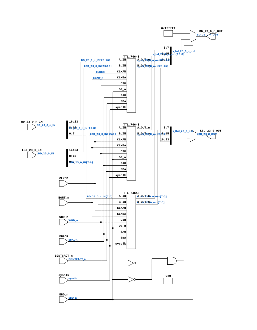
Contains: TTL_74648 x3
Module hierarchy - All modules
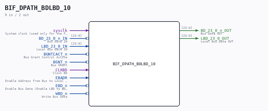
Schematic
Drawn from the Verilog: the yosys netlist of the Simulation (Verilator) build, instance CORE.CPU_BOARD.BIF.DPATH.BDLBD. Sub-modules are boxes (click the picture to open it full size; there every sub-module box links to its page, and every wire shows its Verilog name).
Description
ND120 CPU, MM&M BIF/DPATH/BDLBD BIF BD TO LBD SHEET 10 of 50 Last reviewed: 14-DEC-2024 Ronny Hansen
Ports
| Direction | Width | Name | Description |
|---|---|---|---|
| input | 1 |
sysclk |
System clock (used only for the FF-mode strobe edge-capture) |
| input | [23:0] |
BD_23_0_n_IN |
Bus Data IN |
| output | [23:0] |
BD_23_0_n_OUT |
Bus Data OUT |
| input | [23:0] |
LBD_23_0_IN |
Local Bus Data IN |
| output | [23:0] |
LBD_23_0_OUT |
Local Bus Data OUT |
| input | 1 |
BGNTCACT_n (active low) |
Bus Grant Control Active |
| input | 1 |
BGNT_n (active low) |
Bus GRant |
| input | 1 |
CLKBD |
Clock BD |
| input | 1 |
EBADR |
Enable Address from Bus to Local Memory |
| input | 1 |
EBD_n (active low) |
Enable Bus Data (Enable LBD to BD transceiver). |
| input | 1 |
WBD_n (active low) |
Write Bus Data |
Verilog source
Verilog/CPU-BOARD-3202/circuit/BIF_DPATH_BDLBD_10.v on GitHub.
Show the Verilog of BIF_DPATH_BDLBD_10 (155 lines)
/**************************************************************************
** ND120 CPU, MM&M                                                       **
** BIF/DPATH/BDLBD                                                       **
** BIF BD TO LBD                                                         **
** SHEET 10 of 50                                                        **
**                                                                       **
** Last reviewed: 14-DEC-2024                                            **
** Ronny Hansen                                                          **
***************************************************************************/
module BIF_DPATH_BDLBD_10 (
    input sysclk,  //! System clock (used only for the FF-mode strobe edge-capture)

    input  [23:0] BD_23_0_n_IN,  //! Bus Data IN
    output [23:0] BD_23_0_n_OUT, //! Bus Data OUT

    input  [23:0] LBD_23_0_IN,  //! Local Bus Data IN
    output [23:0] LBD_23_0_OUT, //! Local Bus Data OUT

    input BGNTCACT_n,  //! Bus Grant Control Active
    input BGNT_n,      //! Bus GRant
    input CLKBD,       //! Clock BD
    input EBADR,       //! Enable Address from Bus to Local Memory
    input EBD_n,       //! Enable Bus Data (Enable LBD to BD transceiver).
    input WBD_n        //! Write Bus Data
);


  /*******************************************************************************
   ** The wires are defined here                                                 **
   *******************************************************************************/
  wire [23:0] s_lbd_23_0_in;
  wire [23:0] s_lbd_23_0_out;
  wire [23:0] s_bd_23_0_n_in;
  wire [23:0] s_bd_23_0_n_out;

  wire        s_bgnt_n;
  wire        s_bgntcact_n;
  wire        s_clkbd;
  wire        s_ebadr;
  wire        s_ebd_n;
  wire        s_wbd_n;

  /*******************************************************************************
   ** Here all input connections are defined                                     **
   *******************************************************************************/
  assign s_bd_23_0_n_in[23:0] = BD_23_0_n_IN[23:0];
  assign s_lbd_23_0_in[23:0] = LBD_23_0_IN[23:0];

  assign s_ebadr = EBADR;
  assign s_ebd_n = EBD_n;
  assign s_wbd_n = WBD_n;
  assign s_clkbd = CLKBD;
  assign s_bgntcact_n = BGNTCACT_n;
  assign s_bgnt_n = BGNT_n;

  /*******************************************************************************
   ** Here all output connections are defined                                    **
   *******************************************************************************/
  assign LBD_23_0_OUT = (!s_ebd_n) ? s_lbd_23_0_out[23:0] : 24'b0;
  // A 74AS648 drives its A pins only when OE~ is LOW **and** DIR selects
  // B->A. This line handled the OE~ case alone, so with EBD_n=0 and WBD_n=1 -
  // the read half of every ND-bus cycle - it published 24'h000000, which on
  // this ACTIVE-LOW wired-AND net means the BIF asserting all 24 BD lines,
  // instead of releasing them. The released value for BD is all ones, which
  // the OE~ branch on this same line already uses.
  //
  // TTL_74648.v returns 8'b0 for the DIR-disabled case, and that is correct
  // for the LBD and CD wired-OR nets - it is only wrong for this one
  // active-low net, so the correction belongs here and not in the chip model.
  //
  // It mattered: ND120_CORE hands BD_23_0_n_OUT to the floppy-DMA, SMD,
  // Winchester and DMA models as their bus input, and ND_BUS_SLAVE.v latches
  // ~BD_23_0_n_OUT as the bus address - so a slave sampling during a read
  // window saw 24'hFFFFFF. It also reaches the board pin on the Tang build.
  assign BD_23_0_n_OUT        = (!s_ebd_n && !s_wbd_n) ? s_bd_23_0_n_out[23:0] : ~24'b0;


  /*******************************************************************************
   ** Here all sub-circuits are defined                                          **
   *******************************************************************************/

  // P1d (docs/plan-fix-unconstrained-clocks.md): BGNT_n is a bus-grant
  // strobe, not a clock. In FF mode the CLKBA registers capture on a
  // sysclk-detected BGNT_n rise instead of clocking on the routed net.
  // P3: CLKAB (CLKBD) converted the same way - CLKBD is a bus-data
  // capture strobe, not a clock.
`ifdef FPGA_FF_MODE
  localparam BGNT_CAPTURE = 2;
  localparam CLKBD_CAPTURE = 2;
`else
  localparam BGNT_CAPTURE = 0;
  localparam CLKBD_CAPTURE = 0;
`endif

  TTL_74648 #(.USE_SYSCLK_AB(CLKBD_CAPTURE), .USE_SYSCLK_BA(BGNT_CAPTURE)) CHIP_4A (
      .sysclk(sysclk),
      .A_IN(s_bd_23_0_n_in[23:16]),
      .A_OUT_n(s_bd_23_0_n_out[23:16]),

      .B_IN(s_lbd_23_0_in[23:16]),
      .B_OUT_n(s_lbd_23_0_out[23:16]),


      .CLKAB(s_clkbd),
      .CLKBA(s_bgnt_n),

      .SAB(s_ebadr),
      .SBA(s_bgntcact_n),

      .DIR (s_wbd_n),
      .OE_n(s_ebd_n)
  );


  TTL_74648 #(.USE_SYSCLK_AB(CLKBD_CAPTURE), .USE_SYSCLK_BA(BGNT_CAPTURE)) CHIP_5A (
      .sysclk(sysclk),
      .A_IN(s_bd_23_0_n_in[15:8]),
      .A_OUT_n(s_bd_23_0_n_out[15:8]),

      .B_IN(s_lbd_23_0_in[15:8]),
      .B_OUT_n(s_lbd_23_0_out[15:8]),


      .CLKAB(s_clkbd),
      .CLKBA(s_bgnt_n),

      .SAB(s_ebadr),
      .SBA(s_bgntcact_n),

      .DIR (s_wbd_n),
      .OE_n(s_ebd_n)
  );


  TTL_74648 #(.USE_SYSCLK_AB(CLKBD_CAPTURE), .USE_SYSCLK_BA(BGNT_CAPTURE)) CHIP_6A (
      .sysclk(sysclk),
      .A_IN(s_bd_23_0_n_in[7:0]),
      .A_OUT_n(s_bd_23_0_n_out[7:0]),

      .B_IN(s_lbd_23_0_in[7:0]),
      .B_OUT_n(s_lbd_23_0_out[7:0]),


      .CLKAB(s_clkbd),
      .CLKBA(s_bgnt_n),

      .SAB(s_ebadr),
      .SBA(s_bgntcact_n),

      .DIR (s_wbd_n),
      .OE_n(s_ebd_n)
  );

endmodule