CYC_36
Source: Verilog/CPU-BOARD-3202/circuit/CYC_36.v
Where it sits (Simulation): ND120_TOP > ND120_CORE > ND3202D > CYC_36
- instance path: CORE.CPU_BOARD.CYC
Used in: ND3202D (all tops)
Contains: CYC_CC_D, CYC_TERM_D, PAL_44307C x2, PAL_44403C_EN, PAL_44404C_EN, PAL_44601B
Module hierarchy - All modules
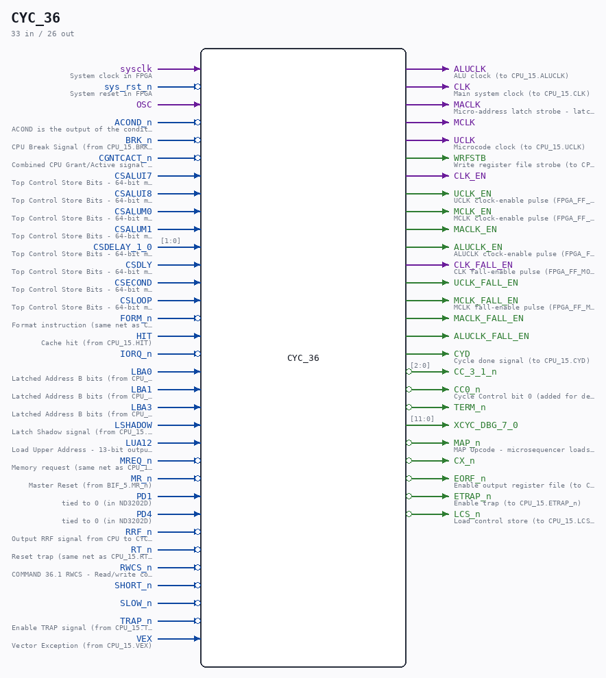
Schematic
Drawn from the Verilog: the yosys netlist of the Simulation (Verilator) build, instance CORE.CPU_BOARD.CYC. Sub-modules are boxes (click the picture to open it full size; there every sub-module box links to its page, and every wire shows its Verilog name).
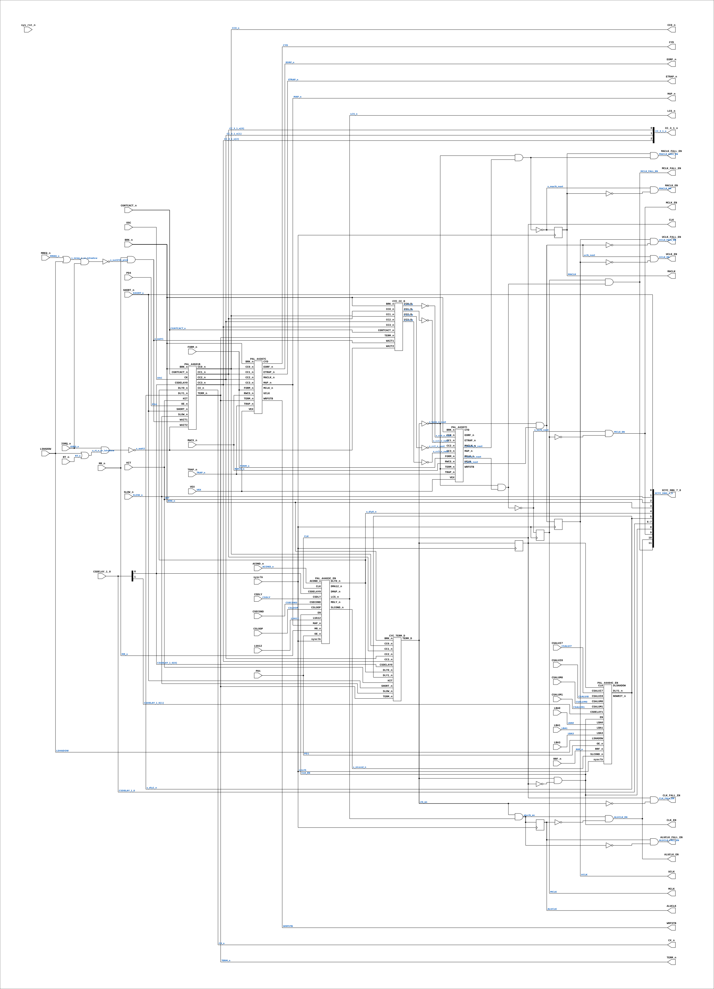
Description
ND120 CPU, MM&M CYC CYCLE CONTROL SHEET 36 of 50 Last reviewed: 9-NOVEMBER-2024 Ronny Hansen
Ports
| Direction | Width | Name | Description |
|---|---|---|---|
| input | 1 |
sysclk |
System clock in FPGA |
| input | 1 |
sys_rst_n (active low) |
System reset in FPGA |
| input | 1 |
OSC |
|
| input | 1 |
ACOND_n (active low) |
ACOND is the output of the condition register. (from CPU_15.ACOND_n) |
| input | 1 |
BRK_n (active low) |
CPU Break Signal (from CPU_15.BRK_n) |
| input | 1 |
CGNTCACT_n (active low) |
Combined CPU Grant/Active signal (from BIF_5.CGNTCACT_n) |
| input | 1 |
CSALUI7 |
Top Control Store Bits - 64-bit microcode control signals (from CPU_15.TOPCSB[62]) |
| input | 1 |
CSALUI8 |
Top Control Store Bits - 64-bit microcode control signals (from CPU_15.TOPCSB[63]) |
| input | 1 |
CSALUM0 |
Top Control Store Bits - 64-bit microcode control signals (from CPU_15.TOPCSB[44]) |
| input | 1 |
CSALUM1 |
Top Control Store Bits - 64-bit microcode control signals (from CPU_15.TOPCSB[45]) |
| input | [1:0] |
CSDELAY_1_0 |
Top Control Store Bits - 64-bit microcode control signals (from CPU_15.TOPCSB[27:26]) |
| input | 1 |
CSDLY |
Top Control Store Bits - 64-bit microcode control signals (from CPU_15.TOPCSB[21]) |
| input | 1 |
CSECOND |
Top Control Store Bits - 64-bit microcode control signals (from CPU_15.TOPCSB[23]) |
| input | 1 |
CSLOOP |
Top Control Store Bits - 64-bit microcode control signals (from CPU_15.TOPCSB[22]) |
| input | 1 |
FORM_n (active low) |
Format instruction (same net as CPU_15.FORM_n) |
| input | 1 |
HIT |
Cache hit (from CPU_15.HIT) |
| input | 1 |
IORQ_n (active low) |
|
| input | 1 |
LBA0 |
Latched Address B bits (from CPU_15.LBA_3_0[0]) |
| input | 1 |
LBA1 |
Latched Address B bits (from CPU_15.LBA_3_0[1]) |
| input | 1 |
LBA3 |
Latched Address B bits (from CPU_15.LBA_3_0[3]) |
| input | 1 |
LSHADOW |
Latch Shadow signal (from CPU_15.LSHADOW) |
| input | 1 |
LUA12 |
Load Upper Address - 13-bit output for upper address bits of control store (from CPU_15.LUA_12_0[12]) |
| input | 1 |
MREQ_n (active low) |
Memory request (same net as CPU_15.MREQ_n) |
| input | 1 |
MR_n (active low) |
Master Reset (from BIF_5.MR_n) |
| input | 1 |
PD1 |
tied to 0 (in ND3202D) |
| input | 1 |
PD4 |
tied to 0 (in ND3202D) |
| input | 1 |
RRF_n (active low) |
Output RRF signal from CPU to CYCLE (from CPU_15.RRF_n) |
| input | 1 |
RT_n (active low) |
Reset trap (same net as CPU_15.RT_n) |
| input | 1 |
RWCS_n (active low) |
COMMAND 36.1 RWCS - Read/write control store as addressed by ADCS command (from CPU_15.RWCS_n) |
| input | 1 |
SHORT_n (active low) |
|
| input | 1 |
SLOW_n (active low) |
|
| input | 1 |
TRAP_n (active low) |
Enable TRAP signal (from CPU_15.TRAPN) |
| input | 1 |
VEX |
Vector Exception (from CPU_15.VEX) |
| output | 1 |
ALUCLK |
ALU clock (to CPU_15.ALUCLK) |
| output | 1 |
CLK |
Main system clock (to CPU_15.CLK) |
| output | 1 |
MACLK |
Micro-address latch strobe - latch enable for the control-store address latches in CPU_CS_ACAL_17 (transparent high, captures on the FALLING edge). (to CPU_15.MACLK) |
| output | 1 |
MCLK |
|
| output | 1 |
UCLK |
Microcode clock (to CPU_15.UCLK) |
| output | 1 |
WRFSTB |
Write register file strobe (to CPU_15.WRFSTB) |
| output | 1 |
CLK_EN |
|
| output | 1 |
UCLK_EN |
UCLK clock-enable pulse (FPGA_FF_MODE, else 0) (to CPU_15.UCLK_EN) |
| output | 1 |
MCLK_EN |
MCLK clock-enable pulse (FPGA_FF_MODE, else 0) (to CPU_15.MCLK_EN) |
| output | 1 |
MACLK_EN |
|
| output | 1 |
ALUCLK_EN |
ALUCLK clock-enable pulse (FPGA_FF_MODE, else 0) (to CPU_15.ALUCLK_EN) |
| output | 1 |
CLK_FALL_EN |
CLK fall-enable pulse (FPGA_FF_MODE, else 0) (to IO_37.CLK_FALL_EN) |
| output | 1 |
UCLK_FALL_EN |
|
| output | 1 |
MCLK_FALL_EN |
MCLK fall-enable pulse (FPGA_FF_MODE, else 0) (to CPU_15.MCLK_FALL_EN) |
| output | 1 |
MACLK_FALL_EN |
|
| output | 1 |
ALUCLK_FALL_EN |
|
| output | 1 |
CYD |
Cycle done signal (to CPU_15.CYD) |
| output | [2:0] |
CC_3_1_n (active low) |
|
| output | 1 |
CC0_n (active low) |
Cycle Control bit 0 (added for debug) |
| output | 1 |
TERM_n (active low) |
|
| output | [11:0] |
XCYC_DBG_7_0 |
|
| output | 1 |
MAP_n (active low) |
MAP Opcode - microsequencer loads next micro-address from the opcode mapper; last microinstruction of every macro instruction (active low) (to CPU_15.MAP_n) |
| output | 1 |
CX_n (active low) |
|
| output | 1 |
EORF_n (active low) |
Enable output register file (to CPU_15.EORF_n) |
| output | 1 |
ETRAP_n (active low) |
Enable trap (to CPU_15.ETRAP_n) |
| output | 1 |
LCS_n (active low) |
Load control store (to CPU_15.LCS_n) |
Verilog source
Verilog/CPU-BOARD-3202/circuit/CYC_36.v on GitHub.
Show the Verilog of CYC_36 (563 lines)
/**************************************************************************
** ND120 CPU, MM&M                                                       **
** CYC                                                                   **
** CYCLE CONTROL                                                         **
** SHEET 36 of 50                                                        **
**                                                                       **
** Last reviewed: 9-NOVEMBER-2024                                        **
** Ronny Hansen                                                          **
***************************************************************************/


module CYC_36 (
    /* verilator lint_off UNUSEDSIGNAL */
    input sysclk,    // System clock in FPGA
    input sys_rst_n, // System reset in FPGA
    /* verilator lint_on UNUSEDSIGNAL */

    input OSC,

    input ACOND_n,   //! ACOND is the output of the condition register. (from CPU_15.ACOND_n)
    input BRK_n,     //! CPU Break Signal (from CPU_15.BRK_n)
    input CGNTCACT_n,  //! Combined CPU Grant/Active signal (from BIF_5.CGNTCACT_n)
    input CSALUI7,   //! Top Control Store Bits - 64-bit microcode control signals (from CPU_15.TOPCSB[62])
    input CSALUI8,   //! Top Control Store Bits - 64-bit microcode control signals (from CPU_15.TOPCSB[63])
    input CSALUM0,   //! Top Control Store Bits - 64-bit microcode control signals (from CPU_15.TOPCSB[44])
    input CSALUM1,   //! Top Control Store Bits - 64-bit microcode control signals (from CPU_15.TOPCSB[45])
    input [1:0] CSDELAY_1_0,  //! Top Control Store Bits - 64-bit microcode control signals (from CPU_15.TOPCSB[27:26])
    input CSDLY,     //! Top Control Store Bits - 64-bit microcode control signals (from CPU_15.TOPCSB[21])
    input CSECOND,   //! Top Control Store Bits - 64-bit microcode control signals (from CPU_15.TOPCSB[23])
    input CSLOOP,    //! Top Control Store Bits - 64-bit microcode control signals (from CPU_15.TOPCSB[22])
    input FORM_n,    //! Format instruction (same net as CPU_15.FORM_n)
    input HIT,       //! Cache hit (from CPU_15.HIT)
    input IORQ_n,
    input LBA0,      //! Latched Address B bits (from CPU_15.LBA_3_0[0])
    input LBA1,      //! Latched Address B bits (from CPU_15.LBA_3_0[1])
    input LBA3,      //! Latched Address B bits (from CPU_15.LBA_3_0[3])
    input LSHADOW,   //! Latch Shadow signal (from CPU_15.LSHADOW)
    input LUA12,     //! Load Upper Address - 13-bit output for upper address bits of control store (from CPU_15.LUA_12_0[12])
    input MREQ_n,    //! Memory request (same net as CPU_15.MREQ_n)
    input MR_n,      //! Master Reset (from BIF_5.MR_n)
    input PD1,       //! tied to 0 (in ND3202D)
    input PD4,       //! tied to 0 (in ND3202D)
    input RRF_n,     //! Output RRF signal from CPU to CYCLE (from CPU_15.RRF_n)
    input RT_n,      //! Reset trap (same net as CPU_15.RT_n)
    input RWCS_n,    //! COMMAND 36.1 RWCS - Read/write control store as addressed by ADCS command (from CPU_15.RWCS_n)
    input SHORT_n,
    input SLOW_n,
    input TRAP_n,    //! Enable TRAP signal (from CPU_15.TRAPN)
    input VEX,       //! Vector Exception (from CPU_15.VEX)

    // Outputs
    output ALUCLK,   //! ALU clock (to CPU_15.ALUCLK)
    output CLK,      //! Main system clock (to CPU_15.CLK)
    output MACLK,    //! Micro-address latch strobe - latch enable for the control-store address latches in CPU_CS_ACAL_17 (transparent high, captures on the FALLING edge). (to CPU_15.MACLK)
    output MCLK,
    output UCLK,     //! Microcode clock (to CPU_15.UCLK)
    output WRFSTB,   //! Write register file strobe (to CPU_15.WRFSTB)

    // One-sysclk-wide clock-enable pulses (FPGA_FF_MODE only, else tied 0).
    // Each asserts during the sysclk cycle whose POSEDGE is the rising edge
    // of the corresponding phase-accurate clock, so a consumer converted to
    // `posedge sysclk + if (XCLK_EN)` captures on exactly the edge the old
    // `posedge XCLK` flop did. P2 of docs/plan-fix-unconstrained-clocks.md.
    output CLK_EN,
    output UCLK_EN,  //! UCLK clock-enable pulse (FPGA_FF_MODE, else 0) (to CPU_15.UCLK_EN)
    output MCLK_EN,  //! MCLK clock-enable pulse (FPGA_FF_MODE, else 0) (to CPU_15.MCLK_EN)
    output MACLK_EN,
    output ALUCLK_EN,  //! ALUCLK clock-enable pulse (FPGA_FF_MODE, else 0) (to CPU_15.ALUCLK_EN)
    // Matching FALL pulses (level & ~next): high in the cycle whose POSEDGE
    // is the FALLING edge of the phase-accurate clock, for consumers that
    // clocked on the inverted net (posedge ~xclk / InvertClockEnable).
    output CLK_FALL_EN,  //! CLK fall-enable pulse (FPGA_FF_MODE, else 0) (to IO_37.CLK_FALL_EN)
    output UCLK_FALL_EN,
    output MCLK_FALL_EN,  //! MCLK fall-enable pulse (FPGA_FF_MODE, else 0) (to CPU_15.MCLK_FALL_EN)
    output MACLK_FALL_EN,
    output ALUCLK_FALL_EN,
    output CYD,      //! Cycle done signal (to CPU_15.CYD)
    output [2:0] CC_3_1_n,
    output CC0_n,          // Cycle Control bit 0 (added for debug)
    output TERM_n,
    //! DEBUG (01-SEP-2026): the INPUTS the terminate plane is built from, so
    //! the MiSTer board and the simulator can be compared on what drives the
    //! cycle controller rather than on its output. Measured there: the board
    //! does not assert TERM at microcode 001007 and does not assert CC0 at
    //! 001020, where a booting machine does, and its CC state is already
    //! different one microinstruction earlier. See
    //! Verilog/docs/mister-microcode-loop.md.
    //!   [0] SHORT_n  [1] SLOW_n  [2] HIT   [3] BRK_n
    //!   [4] DLY0_n   [5] DLY1_n  [7:6] CSDELAY_1_0
    //! Read-only fan-out; adds no logic.
    //!   [8] CLK_EN [9] MCLK_EN [10] ALUCLK_EN - the clock-enable pulses the
    //!   cycle-control register actually steps on. Added after the board was
    //!   found taking a DIFFERENT CC state from IDENTICAL inputs, which is
    //!   either different clocking or different logic; these separate the two.
    output [11:0] XCYC_DBG_7_0,
    output MAP_n,    //! MAP Opcode - microsequencer loads next micro-address from the opcode mapper; last microinstruction of every macro instruction (active low) (to CPU_15.MAP_n)
    output CX_n,
    output EORF_n,   //! Enable output register file (to CPU_15.EORF_n)
    output ETRAP_n,  //! Enable trap (to CPU_15.ETRAP_n)
    output LCS_n     //! Load control store (to CPU_15.LCS_n)
);

  /*******************************************************************************
   ** The wires are defined here                                                 **
   *******************************************************************************/
  wire [1:0] s_csdelay_1_0;
  wire [2:0] s_cc_3_1_n;

  wire       c_csdly;
  wire       s_acond_n;
  wire       s_aluclk;
  wire       s_brk_n;
  (* mark_debug = "true" *) wire s_cc0_n;
  wire       s_cgntcact_n;
  wire       s_clk;
  wire       s_clk_ce_en;
  wire       s_csalui7;
  wire       s_csalui8;
  wire       s_csalum0;
  wire       s_csalum1;
  wire       s_csecond;
  wire       s_csloop;
  wire       s_cx_n;
  wire       s_cyd;
  wire       s_dly0_n;
  wire       s_dly1_n;
  wire       s_eorf_n;
  wire       s_etrap_n;
  wire       s_form_n;
  wire       s_hit;
  wire       s_iorq_n;
  wire       s_lba0;
  wire       s_lba1;
  wire       s_lba3;
  wire       s_lcs_n;
  wire       s_lcs;
  wire       s_lshadow;
  wire       s_lua12;
  wire       s_maclk_n;
  wire       s_maclk_out;
  wire       s_map_n;
  wire       s_mclk_n;
  wire       s_mclk;
  wire       s_mr_n;
  wire       s_mreq_n_or_lshadow;
  wire       s_mreq_n;
  wire       s_osc;
  wire       s_out25h_pin6;
  wire       s_pd1;
  wire       s_pd4;
  wire       s_RRF_n;
  wire       s_rt_n_or_lshadow;
  wire       s_rt_n;
  wire       s_rwcs_n;
  wire       s_short_n;
  wire       s_slcond_n;
  wire       s_slow_n;
  wire       s_term_n;
  wire       s_trap_n;
  wire       s_uclk_out;
  wire       s_uclk;
  wire       s_vex;
  wire       s_wait1;
  wire       s_wait2;
  wire       s_wrfstb;


  /*******************************************************************************
   ** Here all input connections are defined                                     **
   *******************************************************************************/
  assign c_csdly             = CSDLY;
  assign s_acond_n           = ACOND_n;
  assign s_brk_n             = BRK_n;
  assign s_cgntcact_n        = CGNTCACT_n;
  assign s_csalui7           = CSALUI7;
  assign s_csalui8           = CSALUI8;
  assign s_csalum0           = CSALUM0;
  assign s_csalum1           = CSALUM1;
  assign s_csdelay_1_0[1:0]  = CSDELAY_1_0[1:0];
  assign s_csecond           = CSECOND;
  assign s_csloop            = CSLOOP;
  assign s_form_n            = FORM_n;
  assign s_hit               = HIT;
  assign s_iorq_n            = IORQ_n;
  assign s_lba0              = LBA0;
  assign s_lba1              = LBA1;
  assign s_lba3              = LBA3;
  assign s_lshadow           = LSHADOW;
  assign s_lua12             = LUA12;
  assign s_mr_n              = MR_n;
  assign s_mreq_n            = MREQ_n;
  assign s_osc               = OSC;
  assign s_pd1               = PD1;
  assign s_pd4               = PD4;
  assign s_RRF_n             = RRF_n;
  assign s_rt_n              = RT_n;
  assign s_rwcs_n            = RWCS_n;
  assign s_short_n           = SHORT_n;
  assign s_slow_n            = SLOW_n;
  assign s_trap_n            = TRAP_n;
  assign s_vex               = VEX;

  /*******************************************************************************
   ** Here all output connections are defined                                    **
   *******************************************************************************/
`ifdef FPGA_FF_MODE
  // ---- Phase-accurate ALUCLK (single sysclk domain) ----
  // ALUCLK = ~(TERM_n|LCS) pulses at bus-cycle terminate; the ALU / condition
  // register latch on its rising edge. To move off the gated combinational clock
  // without shifting that latch, we need the enable to fire on the SAME sysclk
  // edge the old ALUCLK did. CYC_TERM_D gives TERM's NEXT-state (validated exactly
  // == PAL_44601B, see CYC_TERM_D_tb.v), which is high the cycle BEFORE TERM
  // asserts; registering it lands aluclk_pa's rising edge on the correct edge
  // (net-zero latency vs the +1 of registering the already-risen s_aluclk).
  // Clean FF-generated clock, no consumer edits. See docs/clock-enable-refactor.md.
  wire s_term_d;
  CYC_TERM_D U_TERM_D (
      .CC0_n  (s_cc0_n),
      .CC1_n  (s_cc_3_1_n[0]),
      .CC2_n  (s_cc_3_1_n[1]),
      .CC3_n  (s_cc_3_1_n[2]),
      .TERM_n (s_term_n),
      .SHORT_n(s_short_n),
      .HIT    (s_hit),
      .BRK_n  (s_brk_n),
      .SLOW_n (s_slow_n),
      .DLY0_n (s_dly0_n),
      .DLY1_n (s_dly1_n),
      .CSDELAY0(s_csdelay_1_0[0]),
      .TERM_D (s_term_d)
  );
  wire aluclk_en = s_term_d & ~s_lcs;   // ALUCLK about to rise (LCS gates it off during load)
  reg  aluclk_pa = 1'b0;
  always @(posedge sysclk) aluclk_pa <= aluclk_en;
  assign ALUCLK              = aluclk_pa;

  // ---- Phase-accurate MCLK / MACLK ----
  // MCLK/MACLK = ~(TERM_n & MCLK_n/MACLK_n); MCLK_n/MACLK_n are combinational
  // PAL_44307C decodes of CC + TERM. Feed a SECOND (combinational) PAL_44307C
  // the NEXT-state - TERM from CYC_TERM_D, CC from CYC_CC_D (both validated ==
  // PAL_44601B) - to get their next values, then fire each enable on the edge
  // the old clock rose. The PALs stay untouched; PAL_44307C is reused as-is.
  wire s_cc0_d, s_cc1_d, s_cc2_d, s_cc3_d;
  CYC_CC_D U_CC_D (
      .CC0_n     (s_cc0_n),
      .CC1_n     (s_cc_3_1_n[0]),
      .CC2_n     (s_cc_3_1_n[1]),
      .CC3_n     (s_cc_3_1_n[2]),
      .TERM_n    (s_term_n),
      .CGNTCACT_n(s_cgntcact_n),
      .WAIT1     (s_wait1),
      .WAIT2     (s_wait2),
      .BRK_n     (s_brk_n),
      .CC0_D     (s_cc0_d),
      .CC1_D     (s_cc1_d),
      .CC2_D     (s_cc2_d),
      .CC3_D     (s_cc3_d)
  );
  wire s_term_n_next = ~s_term_d;
  wire s_cc0_n_next  = ~s_cc0_d;
  wire s_cc1_n_next  = ~s_cc1_d;
  wire s_cc2_n_next  = ~s_cc2_d;
  wire s_cc3_n_next  = ~s_cc3_d;
  wire s_mclk_n_next, s_maclk_n_next, s_uclk_next;
  /* verilator lint_off PINCONNECTEMPTY */
  PAL_44307C PAL_44307_UCYCLK_NEXT (
      .TERM_n (s_term_n_next),
      .CC0_n  (s_cc0_n_next),
      .CC1_n  (s_cc1_n_next),
      .CC2_n  (s_cc2_n_next),
      .CC3_n  (s_cc3_n_next),
      .FORM_n (s_form_n),
      .BRK_n  (s_brk_n),
      .RWCS_n (s_rwcs_n),
      .TRAP_n (s_trap_n),
      .VEX    (s_vex),
      .MCLK_n (s_mclk_n_next),
      .MACLK_n(s_maclk_n_next),
      .UCLK   (s_uclk_next),
      .WRFSTB (), .CYD (), .EORF_n (), .ETRAP_n (), .MAP_n ()
  );
  /* verilator lint_on PINCONNECTEMPTY */
  wire s_mclk_next  = ~(s_term_n_next & s_mclk_n_next);   // next MCLK  = ~(TERM_n_next & MCLK_n_next)
  wire s_maclk_next = ~(s_term_n_next & s_maclk_n_next);  // next MACLK
  // Register the predicted next LEVEL, not a rise-only pulse. The rising edge
  // lands on the same sysclk edge as the original gated clock (same property
  // the pulse form had), but the full high phase is also reproduced. That
  // matters for level consumers: CPU_CS_ACAL_17's address latches are
  // transparent while MACLK is HIGH - with a 1-sysclk pulse the WCS address
  // (LUA) froze for the rest of the microcycle, so a mid-cycle CSA change
  // (DGA dispatch via WCA, e.g. instruction-fetch MAP) never reached the WCS
  // and MASEL captured a jump target from the stale previous microword.
  reg  mclk_pa = 1'b0, maclk_pa = 1'b0;
  always @(posedge sysclk) begin
    mclk_pa  <= s_mclk_next;
    maclk_pa <= s_maclk_next;
  end
  assign MCLK                = mclk_pa;
  assign MACLK               = maclk_pa;

  // ---- Phase-accurate CLK and UCLK ----
  // CLK = ~TERM_n rises at terminate (like ALUCLK but without the LCS gate), so
  // clk_en = TERM_d. CLK also clocks the FSM's own PAL_44403/44404 (via s_clk),
  // so those PALs now run on the clean generated clock instead of the gated net -
  // the PALs themselves are untouched, only their clock input changes.
  // UCLK = TERM_n & UCLK_44307 has its own mid-cycle phase; uclk_next uses the
  // 2nd PAL_44307's UCLK on the next-state.
  wire clk_en   = s_term_d;                       // CLK next level = TERM_D (high while TERM asserted)
  wire uclk_next = s_term_n_next & s_uclk_next;   // next UCLK = TERM_n_next & UCLK_44307_next
  // Same level-accurate treatment as MCLK/MACLK above: register the predicted
  // next LEVEL so the full UCLK high phase is reproduced, not just the rise.
  reg  clk_pa = 1'b0, uclk_pa = 1'b0;
  always @(posedge sysclk) begin
    clk_pa  <= clk_en;
    uclk_pa <= uclk_next;
  end
  assign UCLK                = uclk_pa;

  // ---- Clock-enable pulses for P2 domain conversions ----
  // next-level & ~current-level = high exactly in the cycle before the pa
  // clock's rise, i.e. the enable is sampled by the SAME sysclk posedge
  // that produces the rise. Consumers on `posedge sysclk + if (EN)` are
  // then cycle-identical to `posedge pa-clock` flops (same-domain data).
  assign s_clk_ce_en         = clk_en       & ~clk_pa;
  assign CLK_EN              = s_clk_ce_en;
  assign UCLK_EN             = uclk_next    & ~uclk_pa;
  assign MCLK_EN             = s_mclk_next  & ~mclk_pa;
  assign MACLK_EN            = s_maclk_next & ~maclk_pa;
  assign ALUCLK_EN           = aluclk_en    & ~aluclk_pa;
  // FALL pulses: level & ~next = high exactly in the cycle before the pa
  // clock's fall, sampled by the same posedge that produces the fall.
  assign CLK_FALL_EN         = clk_pa    & ~clk_en;
  assign UCLK_FALL_EN        = uclk_pa   & ~uclk_next;
  assign MCLK_FALL_EN        = mclk_pa   & ~s_mclk_next;
  assign MACLK_FALL_EN       = maclk_pa  & ~s_maclk_next;
  assign ALUCLK_FALL_EN      = aluclk_pa & ~aluclk_en;
`else
  assign ALUCLK              = s_aluclk;
  assign MCLK                = s_mclk;
  assign MACLK               = s_maclk_out;
  assign UCLK                = s_uclk_out;
  // Latch mode has no phase-accurate registers: no enables.
  assign s_clk_ce_en         = 1'b0;
  assign CLK_EN              = s_clk_ce_en;
  assign UCLK_EN             = 1'b0;
  assign MCLK_EN             = 1'b0;
  assign MACLK_EN            = 1'b0;
  assign ALUCLK_EN           = 1'b0;
  assign CLK_FALL_EN         = 1'b0;
  assign UCLK_FALL_EN        = 1'b0;
  assign MCLK_FALL_EN        = 1'b0;
  assign MACLK_FALL_EN       = 1'b0;
  assign ALUCLK_FALL_EN      = 1'b0;
`endif
  assign CC_3_1_n            = s_cc_3_1_n[2:0];
  assign CC0_n               = s_cc0_n;
  assign CLK                 = s_clk;
  assign CX_n                = s_cx_n;
  assign CYD                 = s_cyd;
  assign EORF_n              = s_eorf_n;
  assign ETRAP_n             = s_etrap_n;
  assign LCS_n               = s_lcs_n;
  assign MAP_n               = s_map_n;
  assign TERM_n              = s_term_n;

  // DEBUG: the terminate plane's inputs - see the XCYC_DBG_7_0 port comment.
  // [11] MCLK_FALL_EN: the enable the MICROCODE STACK shifts on
  // (CGA_MIC_STACK_BIT SR44_EN). Added 01-SEP-2026: the board returns from a
  // nested microsubroutine to the WRONG address (001015 instead of 002027),
  // which is what a stack that never shifts would do.
  assign XCYC_DBG_7_0 = {MCLK_FALL_EN, ALUCLK_EN, MCLK_EN, CLK_EN,
                         s_csdelay_1_0[1:0], s_dly1_n, s_dly0_n,
                         s_brk_n, s_hit, s_slow_n, s_short_n};
  // MCLK / MACLK / UCLK are assigned in the FPGA_FF_MODE block above
  // (phase-accurate) and in its `else` branch (original gated nets).
  assign WRFSTB              = s_wrfstb;

  /*******************************************************************************
   ** Refactored all gates to use Verilog code for and/or/not                    **
   *******************************************************************************/
  assign s_lcs               = ~s_lcs_n;
`ifdef FPGA_FF_MODE
  // Clean phase-accurate CLK: drives the output CLK and the FSM's own
  // PAL_44403/44404 clock inputs, replacing the gated ~TERM_n net.
  assign s_clk               = clk_pa;
`else
  assign s_clk               = ~s_term_n;
`endif
  assign s_aluclk            = ~(s_term_n | s_lcs);
  assign s_mclk              = ~(s_term_n & s_mclk_n);
  assign s_maclk_out         = ~(s_term_n & s_maclk_n);
  assign s_uclk_out          = (s_term_n & s_uclk);


  assign s_rt_n_or_lshadow   = (s_lshadow | s_rt_n);
  assign s_mreq_n_or_lshadow = (s_mreq_n | s_lshadow);
  assign s_out25h_pin6       = ~(s_mreq_n_or_lshadow & s_iorq_n);

  assign s_wait1             = (s_mr_n & s_out25h_pin6);
  assign s_wait2             = ~(s_iorq_n & s_rt_n_or_lshadow);

  /*******************************************************************************
   ** Here all sub-circuits are defined                                          **
   *******************************************************************************/

  PAL_44601B PAL_44601_UCYCFSM (
      .CK  (s_osc),  //CK
      .OE_n(s_pd4),  //OE_n

      //I0-I7
      .DLY1_n    (s_dly1_n),          //I0 - Delay 1 signal
      .DLY0_n    (s_dly0_n),          //I1 - Delay 0 signal
      .CSDELAY0  (s_csdelay_1_0[0]),  //I2 - Control Store Delay bit 0
      .WAIT1     (s_wait1),           //I3 - Wait state 1 (memory read & !lshadow)
      .WAIT2     (s_wait2),           //I4 - Wait state 2 (!IO request & !reset/lshadow)
      .CGNTCACT_n(s_cgntcact_n),      //I5 - CGNTCACT_n - Combined CPU Grant/Active signal
      .HIT       (s_hit),             //I6 - Cache hit signal
      .BRK_n     (s_brk_n),           //I7 - Break signal, active low

      // B0-B1
      .SLOW_n (s_slow_n),  //B0
      .SHORT_n(s_short_n), //B1

      // Output signals
      //Q0-Q5 (clocked and 3-state)
      .CX_n  (s_cx_n),         //Q0 0=FAST VERSION/CX, 1=SLOW
      .TERM_n(s_term_n),       //Q1 Terminate Bus Cycle
      .CC0_n (s_cc0_n),        //Q2 Cycle Control 0
      .CC1_n (s_cc_3_1_n[0]),  //Q3 Cycle Control 1
      .CC2_n (s_cc_3_1_n[1]),  //Q4 Cycle Control 2
      .CC3_n (s_cc_3_1_n[2])   //Q5 Cycle Control 3
  );

  PAL_44307C PAL_44307_UCYCLK (
      .TERM_n (s_term_n),       // I0  - Terminate bus cycle
      .CC0_n  (s_cc0_n),        // I1  - Cycle Control bit 0
      .CC1_n  (s_cc_3_1_n[0]),  // I2  - Cycle Control bit 1
      .CC2_n  (s_cc_3_1_n[1]),  // I3  - Cycle Control bit 2
      .CC3_n  (s_cc_3_1_n[2]),  // I4  - Cycle Control bit 3
      .FORM_n (s_form_n),       // I5  - Format signal for instruction decoding
      .BRK_n  (s_brk_n),        // I6  - Break signal for debugging
      .RWCS_n (s_rwcs_n),       // I7  - Read/Write Control Store signal
      .TRAP_n (s_trap_n),       // I8  - Trap condition signal
      .VEX    (s_vex),          // I9  - Vector Exception signal (disable traps)
      .MCLK_n (s_mclk_n),       // Y0_n - Microcycle clock output (active low)
      .MACLK_n(s_maclk_n),      // Y1_n - Micro-address latch strobe (active low) - ACAL latch enable
      .WRFSTB (s_wrfstb),       // B0_n - Write Fast Strobe signal
      .CYD    (s_cyd),          // B1_n - Cycle Done indicator
      .EORF_n (s_eorf_n),       // B2_n - End Of Read Format signal (active low)
      .UCLK   (s_uclk),         // B3_n - Microcode Clock signal
      .ETRAP_n(s_etrap_n),      // B4_n - Enable Trap signal - Disabled during t and a cycles and VEX
      .MAP_n  (s_map_n)         // B5_n - MAP Opcode (active low)
  );

  // P2 (docs/plan-fix-unconstrained-clocks.md): the two CYIN PALs register
  // on CLK (= clk_pa in FF mode) and sample converted-domain outputs
  // (ACOND_n from CONDREG, LBA/LSHADOW from MIC/IDBCTL) - they are part of
  // the coupled clock group and convert with it.
`ifdef FPGA_FF_MODE
  localparam CLK_CE = 1;
`else
  localparam CLK_CE = 0;
`endif

  /* verilator lint_off PINMISSING */
  PAL_44403C_EN #(.USE_ENABLE(CLK_CE)) PAL_44403_UCYIN0 (
      .sysclk(sysclk),
      .EN  (s_clk_ce_en),
      .CLK (s_clk),  //CK
      .OE_n(s_pd1),  //OE_n


      .CSDELAY0(s_csdelay_1_0[0]),  //I0
      .CSDLY   (c_csdly),           //I1
      .CSECOND (s_csecond),         //I2
      .CSLOOP  (s_csloop),          //I3
      .ACOND_n (s_acond_n),         //I4
      .MR_n    (s_mr_n),            //I5
      .LUA12   (s_lua12),           //I6
      .MAP_n   (s_map_n),           //I7

      //Q0-Q3 (clocked and 3-state)
      .LCS_n(s_lcs_n),      //Q0_n
      .MDLY_n(),            //Q1_n  (not used)
      .DMA12_n(),           //Q2_n  (not used)
      .DMAP_n(),            //Q3_n  (not used)

      .DLY0_n  (s_dly0_n),   //B0_n
      .SLCOND_n(s_slcond_n)  //B2_n
  );

  PAL_44404C_EN #(.USE_ENABLE(CLK_CE)) PAL_44404_UCYIN1 (
      .sysclk(sysclk),
      .EN  (s_clk_ce_en),
      .CLK (s_clk),  //CK
      .OE_n(s_pd1),  //OE_n

      .CSDELAY1(s_csdelay_1_0[1]),  //I0
      .CSALUM1 (s_csalum1),         //I1
      .CSALUM0 (s_csalum0),         //I2
      .CSALUI8 (s_csalui8),         //I3
      .CSALUI7 (s_csalui7),         //I4
      .LBA3    (s_lba3),            //I5
      .LBA1    (s_lba1),            //I6
      .LBA0    (s_lba0),            //I7

      //Q0-Q3 (clocked and 3-state)
      .NOWRIT_n(),            // Q0_n (not used)
      .DLSHADOW(),            // Q1_n (not used)

      .RRF_n   (s_RRF_n),     // B0_n
      .LSHADOW (s_lshadow),   // B1_n
      .SLCOND_n(s_slcond_n),  // B2_n
      .DLY1_n  (s_dly1_n)     // B3_n
  );

`ifdef PTDBG
  // ------------------------------------------------------------------
  // ETRAP-BLOCK PROBE (inert unless -DPTDBG). 18-AUG-2026.
  //
  // WHAT IT ANSWERS. Measured in Verilator: across 200 consecutive page-fault
  // windows the trap NEVER dispatches - TRAPN never goes low at any point while
  // PGF is asserted. Derived from CGA_TRAP_BRKDET.v GATES_16
  // (TRAPN = brk_n | cbrk | etrap_n) with brk_n=0 and cbrk=0 measured, that
  // means ETRAP_n was HIGH - traps disabled - for the whole window.
  //
  // ETRAP_n comes from PAL_44307C.v:125, which is a faithful copy of the
  // original PAL and is NOT to be "fixed":
  //
  //   ETRAP_n = ~( TERM_n & VEX_n & (CC3 | CC2 | CC1 | CC0) )
  //   ; ENABLE TRAPS ONLY OUTSIDE t OR a
  //   ; UNSTABLE TRAP IN THIS PERIOD CAN DESTROY MA !
  //
  // So ETRAP_n is high when TERM_n=0, or VEX=1, or all four CC bits are 0.
  // This probe logs which of those actually holds while a break is pending, so
  // the defect can be named instead of guessed.
  //
  // Triggered on BRK_n low rather than on PGF, because PGF lives in the CGA and
  // BRK_n is already an input here. Caveat: BRK_n also rises for the other
  // break sources (IPV, WIP, RD2, RV3, CBRK), so a line is not PROOF of a page
  // fault - correlate with the [pgf] records from the CGA probe.
  //
  // Edge-filtered and hard-capped: an unfiltered probe wrote 327 MB in 2.5
  // minutes earlier in this investigation.
  localparam ETRAPDBG_MAX = 60;
  reg [31:0] r_etd_n    = 0;
  reg [5:0]  r_etd_prev = 6'h3F;
  wire [5:0] w_etd_now  = {s_term_n, s_vex, s_cc_3_1_n[2], s_cc_3_1_n[1],
                           s_cc_3_1_n[0], s_cc0_n};
  always @(posedge sysclk) begin
    if (!s_brk_n && s_etrap_n && r_etd_n < ETRAPDBG_MAX &&
        w_etd_now != r_etd_prev) begin
      r_etd_n    <= r_etd_n + 1;
      r_etd_prev <= w_etd_now;
      $display("[etrap] #%0d BRKpending ETRAPn=1 TERMn=%b VEX=%b CC3n=%b CC2n=%b CC1n=%b CC0n=%b",
               r_etd_n, s_term_n, s_vex, s_cc_3_1_n[2], s_cc_3_1_n[1],
               s_cc_3_1_n[0], s_cc0_n);
    end
  end
`endif

endmodule