PAL_44601B
Source: Verilog/PAL/PAL_44601B.v
Where it sits (Simulation): ND120_TOP > ND120_CORE > ND3202D > CYC_36 > PAL_44601B
- instance path: CORE.CPU_BOARD.CYC.PAL_44601_UCYCFSM
Used in: CYC_36 (all tops)
Contains: no other modules.
Module hierarchy - All modules
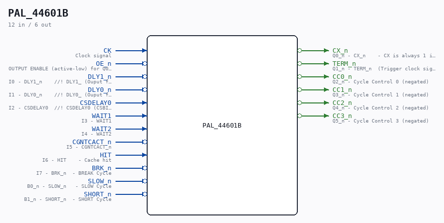
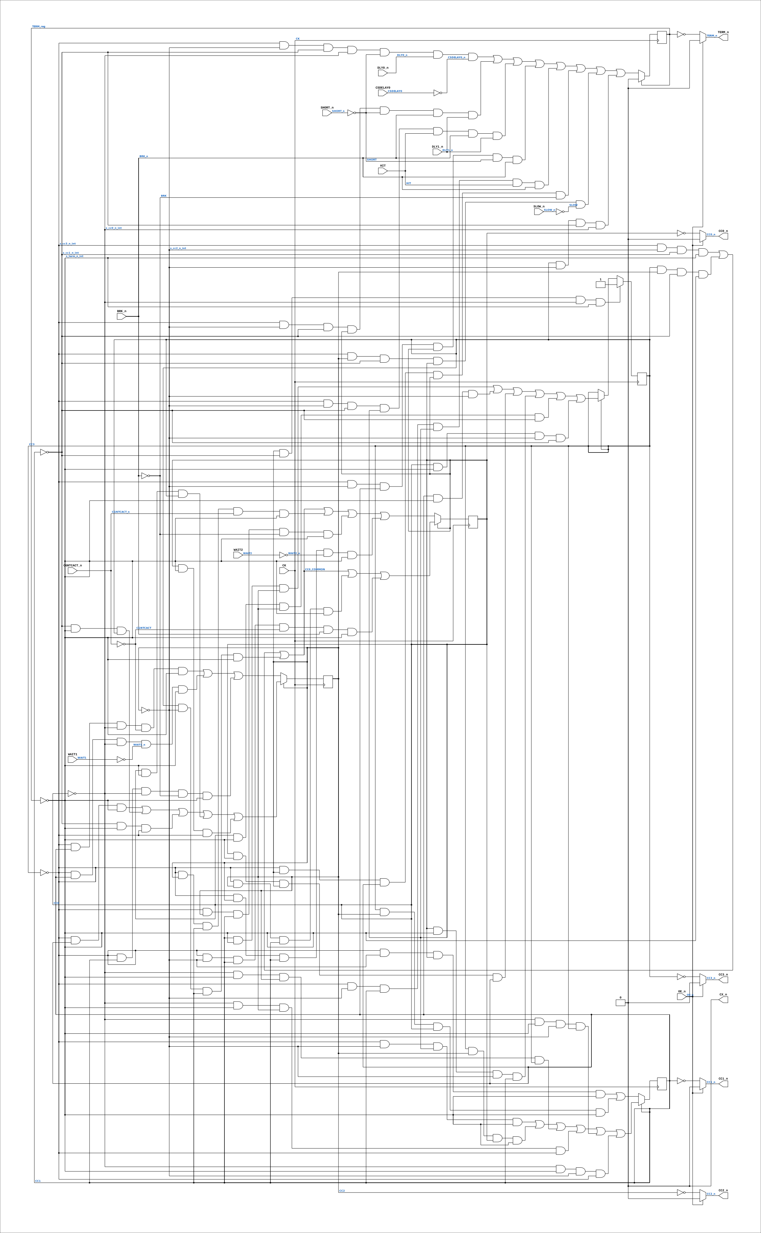
Schematic
Drawn from the Verilog: the yosys netlist of the Simulation (Verilator) build, instance CORE.CPU_BOARD.CYC.PAL_44601_UCYCFSM. Sub-modules are boxes (click the picture to open it full size; there every sub-module box links to its page, and every wire shows its Verilog name).
Description
ND120 PALASM CODE CONVERTED TO VERILOG Component PAL 44601B Last reviewed: 9-FEB-2025 Ronny Hansen
Ports
| Direction | Width | Name | Description |
|---|---|---|---|
| input | 1 |
CK |
Clock signal |
| input | 1 |
OE_n (active low) |
OUTPUT ENABLE (active-low) for Q0-Q5 |
| input | 1 |
DLY1_n (active low) |
I0 - DLY1_n //! DLY1_ (Ouput from PAL 44404 DLY1_n (B3) |
| input | 1 |
DLY0_n (active low) |
I1 - DLY0_n //! DLY0_ (Ouput from PAL 44403 DLY0_n (B0) |
| input | 1 |
CSDELAY0 |
I2 - CSDELAY0 //! CSDELAY0 (CSBITS #26 - DELAY 0) |
| input | 1 |
WAIT1 |
I3 - WAIT1 |
| input | 1 |
WAIT2 |
I4 - WAIT2 |
| input | 1 |
CGNTCACT_n (active low) |
I5 - CGNTCACT_n |
| input | 1 |
HIT |
I6 - HIT - Cache hit |
| input | 1 |
BRK_n (active low) |
I7 - BRK_n - BREAK Cycle |
| input | 1 |
SLOW_n (active low) |
B0_n - SLOW_n - SLOW Cycle |
| input | 1 |
SHORT_n (active low) |
B1_n - SHORT_n - SHORT Cycle |
| output | 1 |
CX_n (active low) |
Q0_n - CX_n - CX is always 1 in the fast version (CX_n = 0) |
| output | 1 |
TERM_n (active low) |
Q1_n - TERM_n (Trigger clock signal that latches CS input signals and more) |
| output | 1 |
CC0_n (active low) |
Q2_n - Cycle Control 0 (negated) |
| output | 1 |
CC1_n (active low) |
Q3_n - Cycle Control 1 (negated) |
| output | 1 |
CC2_n (active low) |
Q4_n - Cycle Control 2 (negated) |
| output | 1 |
CC3_n (active low) |
Q5_n - Cycle Control 3 (negated) |
Verilog source
Verilog/PAL/PAL_44601B.v on GitHub.
Show the Verilog of PAL_44601B (281 lines)
/**********************************************************************************************************
** ND120 PALASM CODE CONVERTED TO VERILOG                                                                **
**                                                                                                       **
** Component PAL 44601B                                                                                  **
**                                                                                                       **
** Last reviewed: 9-FEB-2025                                                                             **
** Ronny Hansen                                                                                          **
***********************************************************************************************************/

// PAL16R6
// JLB 26NOV86
// 44601B, 12D, CYCFSM

//  CYCLE CONTROL STATE COUNTER. FAST VERSION (ND-120/CX).

// PAL16R8 FAMILY
// PAL16R6 has 6 flip-flips, 8 inputs, and 2 input OR output (B0 and B1)

// https://rocelec.widen.net/view/pdf/c6dwcslffz/VANTS00080-1.pdf


// PCB 3202D sheet 36:
//
// PAL input signal PD4 is connected to PAL OE_n pin
//     input signal OSC is connectec to PAL CK pin


module PAL_44601B (
    input CK,   // Clock signal
    input OE_n, // OUTPUT ENABLE (active-low) for Q0-Q5

    input DLY1_n,      //! I0 - DLY1_n    //! DLY1_ (Ouput from PAL 44404 DLY1_n (B3)
    input DLY0_n,      //! I1 - DLY0_n    //! DLY0_ (Ouput from PAL 44403 DLY0_n (B0)
    input CSDELAY0,    //! I2 - CSDELAY0  //! CSDELAY0 (CSBITS #26 - DELAY 0)
    input WAIT1,       //! I3 - WAIT1
    input WAIT2,       //! I4 - WAIT2
    input CGNTCACT_n,  //! I5 - CGNTCACT_n
    input HIT,         //! I6 - HIT    - Cache hit
    input BRK_n,       //! I7 - BRK_n  - BREAK Cycle

    input SLOW_n,  //! B0_n - SLOW_n   - SLOW Cycle
    input SHORT_n, //! B1_n - SHORT_n  - SHORT Cycle

    output CX_n,    //! Q0_n - CX_n    - CX is always 1 in the fast version (CX_n = 0)
    output TERM_n,  //! Q1_n - TERM_n  (Trigger clock signal that latches CS input signals and more)
    output CC0_n,   //! Q2_n - Cycle Control 0 (negated)
    output CC1_n,   //! Q3_n - Cycle Control 1 (negated)
    output CC2_n,   //! Q4_n - Cycle Control 2 (negated)
    output CC3_n    //! Q5_n - Cycle Control 3 (negated)
);

  // Internal registers
  reg  TERM_reg;
  reg  CC0_reg;
  reg  CC1_reg;
  reg  CC2_reg;
  reg  CC3_reg;


  // negated input signals
  wire CSDELAY0_n = ~CSDELAY0;
  wire WAIT1_n = ~WAIT1;
  wire CGNTCACT = ~CGNTCACT_n;
  wire BRK = ~BRK_n;
  wire WAIT2_n = ~WAIT2;

  wire SHORT = ~SHORT_n;
  wire SLOW = ~SLOW_n;

  // Internal register-direct wires -- avoids combinational loop through output ports.
  // In the real PAL16R6, registered outputs feed back internally before the output buffer.
  wire s_term_n_int = ~TERM_reg;  // Internal TERM_n (same value, no output port loop)
  wire CC3 = CC3_reg;
  wire CC2 = CC2_reg;
  wire CC1 = CC1_reg;
  wire CC0 = CC0_reg;
  wire s_cc3_n_int = ~CC3_reg;
  wire s_cc2_n_int = ~CC2_reg;
  wire s_cc1_n_int = ~CC1_reg;
  wire s_cc0_n_int = ~CC0_reg;

  wire CC0_COMMON;

   // Statement both in CC0=1 and CC0=0
  assign CC0_COMMON =
      (s_cc3_n_int & s_cc2_n_int & s_cc1_n_int & s_term_n_int)  // a+b+f+i+j+m+N
    | (CC3 & CC2 & s_cc1_n_int & s_term_n_int)
    | (CC3 & s_cc2_n_int & CC1 & s_term_n_int);


  //**** Sequential logic triggered on the rising edge of CLK ****
  always @(posedge CK) begin

  /********************************************************
  *               TERM                                     *
  *********************************************************/

  /*
    TERM_reg <=   (s_cc3_n_int & s_cc2_n_int  & s_cc1_n_int   & s_cc0_n_int   & SHORT   & s_term_n_int  & DLY0_n & CSDELAY0_n)  // 50NS CYCLE  '0000
                | (s_cc3_n_int & s_cc2_n_int  & s_cc1_n_int   & CC0     & SHORT   & BRK_n   & DLY1_n & s_term_n_int)      // 75NS CYCLE  '0001
                | (s_cc3_n_int & s_cc2_n_int  & s_cc1_n_int   & CC0     & HIT     & BRK_n   & DLY1_n & s_term_n_int)      // 75NS CYCLE  '0001
                | (s_cc3_n_int & s_cc2_n_int  & CC1     & CC0     & SHORT   & BRK_n   & s_term_n_int)  // 100NS CYCLE
                | (s_cc3_n_int & s_cc2_n_int  & CC1     & CC0     & HIT     & BRK_n   & s_term_n_int)  // 100NS CYCLE
                | (s_cc3_n_int & CC2    & CC1     & CC0     & BRK     & s_term_n_int)  // BRK CYCLE  (>200
                | (s_cc3_n_int & CC2    & s_cc1_n_int   & CC0     & SLOW    & s_term_n_int)  // SLOW CYCLES INCL. FE
                | (CC3   & s_cc2_n_int  & s_cc1_n_int   & s_cc0_n_int   & s_term_n_int);  //; UART, LCS, RWCS CYCLES
  */

  if (s_term_n_int) begin
    TERM_reg <=   (s_cc3_n_int & s_cc2_n_int  & s_cc1_n_int   & s_cc0_n_int   & SHORT   & DLY0_n & CSDELAY0_n)  // 50NS CYCLE  '0000
                | (s_cc3_n_int & s_cc2_n_int  & s_cc1_n_int   & CC0     & SHORT   & BRK_n   & DLY1_n )    // 75NS CYCLE  '0001
                | (s_cc3_n_int & s_cc2_n_int  & s_cc1_n_int   & CC0     & HIT     & BRK_n   & DLY1_n )    // 75NS CYCLE  '0001
                | (s_cc3_n_int & s_cc2_n_int  & CC1     & CC0     & SHORT   & BRK_n   )             // 100NS CYCLE
                | (s_cc3_n_int & s_cc2_n_int  & CC1     & CC0     & HIT     & BRK_n   )             // 100NS CYCLE
                | (s_cc3_n_int & CC2    & CC1     & CC0     & BRK     )                       // BRK CYCLE  (>200
                | (s_cc3_n_int & CC2    & s_cc1_n_int   & CC0     & SLOW    )                       // SLOW CYCLES INCL. FE
                | (CC3   & s_cc2_n_int  & s_cc1_n_int   & s_cc0_n_int   );                                //; UART, LCS, RWCS CYCLES
  end else begin
    TERM_reg <= 1'b0;
  end


  /********************************************************
  *               CC3                                     *
  *********************************************************/

  /*
    CC3_reg <= (CC2 & s_cc1_n_int & s_cc0_n_int & s_term_n_int)  // h+i+j+k+l+m+n+o
    | (CC3 & CC1 &  s_term_n_int & CC2)
    | (CC3 & CC1 &  s_term_n_int & s_cc2_n_int)
    | (CC3 & CC0 &  s_term_n_int & CC2 & CC1)
    | (CC3 & CC0 &  s_term_n_int & s_cc2_n_int & CC1)
    | (CC3 & CC0 &  s_term_n_int & CC2 & s_cc1_n_int)
    | (CC3 & CC0 &  s_term_n_int & s_cc2_n_int & s_cc1_n_int);
  */

    if (CC2 & s_cc1_n_int & s_cc0_n_int & s_term_n_int) begin
      CC3_reg <= 1'b1;
    end else begin
      if (CC3_reg) begin
        CC3_reg  <= ( CC1 &  s_term_n_int & CC2)
                  | ( CC1 &  s_term_n_int & s_cc2_n_int)
                  | ( CC0 &  s_term_n_int & CC2 & CC1)
                  | ( CC0 &  s_term_n_int & s_cc2_n_int & CC1)
                  | ( CC0 &  s_term_n_int & CC2 & s_cc1_n_int)
                  | ( CC0 &  s_term_n_int & s_cc2_n_int & s_cc1_n_int);
      end
    end

  /********************************************************
  *               CC2                                      *
  *********************************************************/

/*
    CC2_reg <= (s_cc3_n_int & CC2 & CC1 & s_term_n_int)  // e+f+g+h+i+j+k
    | (CC2 & s_cc1_n_int & s_term_n_int & CC3)
    | (CC2 & s_cc1_n_int & s_term_n_int & s_cc3_n_int)
    | (CC2 & CC0 & s_term_n_int & CC3)
    | (CC2 & CC0 & s_term_n_int & s_cc3_n_int)
    | (s_cc3_n_int & s_cc2_n_int & CC1 & s_cc0_n_int & CGNTCACT & s_term_n_int)  // d WAIT FOR BUS IF
    | (s_cc3_n_int & s_cc2_n_int & CC1 & s_cc0_n_int & WAIT1_n & s_term_n_int)  // d WAIT1 and NOT
    | (s_cc3_n_int & s_cc2_n_int & CC1 & s_cc0_n_int & BRK & s_term_n_int);  // d BRK
*/

    if (CC2) begin
      CC2_reg <=
        (s_cc3_n_int & CC1 & s_term_n_int)  // e+f+g+h+i+j+k
      | ( s_cc1_n_int & s_term_n_int & CC3)
      | ( s_cc1_n_int & s_term_n_int & s_cc3_n_int)
      | ( CC0 & s_term_n_int & CC3)
      | ( CC0 & s_term_n_int & s_cc3_n_int);
    end else begin
      CC2_reg <=
        (s_cc3_n_int & CC1 & s_cc0_n_int & CGNTCACT & s_term_n_int)  // d WAIT FOR BUS IF
      | (s_cc3_n_int & CC1 & s_cc0_n_int & WAIT1_n & s_term_n_int)  // d WAIT1 and NOT
      | (s_cc3_n_int & CC1 & s_cc0_n_int & BRK & s_term_n_int);  // d BRK
    end

  /********************************************************
  *               CC1                                     *
  *********************************************************/

/*
    CC1_reg <= (s_cc3_n_int & s_cc2_n_int & CC0 & s_term_n_int & CC1)  // b+c+d+e+j+k+l+m
    | (s_cc3_n_int & s_cc2_n_int & CC0 & s_term_n_int & s_cc1_n_int)
    | (CC3 & CC2 & CC0 & s_term_n_int & CC1)
    | (CC3 & CC2 & CC0 & s_term_n_int & s_cc1_n_int)
    | (CC1 & s_cc0_n_int & s_term_n_int & CC2 & CC3)
    | (CC1 & s_cc0_n_int & s_term_n_int & CC2 & s_cc3_n_int)
    | (CC1 & s_cc0_n_int & s_term_n_int & s_cc2_n_int & CC3)
    | (CC1 & s_cc0_n_int & s_term_n_int & s_cc2_n_int & s_cc3_n_int);
*/
    if (CC1) begin
      CC1_reg <= (s_cc3_n_int & s_cc2_n_int & CC0 & s_term_n_int)  // b+c+d+e+j+k+l+m
    | (CC3 & CC2 & CC0 & s_term_n_int)
    | (s_cc0_n_int & s_term_n_int & CC2 & CC3)
    | (s_cc0_n_int & s_term_n_int & CC2 & s_cc3_n_int)
    | (s_cc0_n_int & s_term_n_int & s_cc2_n_int & CC3)
    | (s_cc0_n_int & s_term_n_int & s_cc2_n_int & s_cc3_n_int);
    end else begin
      CC1_reg <=
      | (s_cc3_n_int & s_cc2_n_int & CC0 & s_term_n_int)
      | (CC3 & CC2 & CC0 & s_term_n_int);
    end


  /********************************************************
  *               CC0                                     *
  *********************************************************/

    /*
    CC0_reg <= (s_cc3_n_int & s_cc2_n_int & s_cc1_n_int & s_term_n_int)  // a+b+f+i+j+m+N
    | (s_cc3_n_int & CC2 & CC1 & CC0 & s_term_n_int)
    | (CC3 & CC2 & s_cc1_n_int & s_term_n_int)
    | (CC3 & s_cc2_n_int & CC1 & s_term_n_int)
    | (s_cc3_n_int & CC2 & CC1 & s_cc0_n_int & CGNTCACT_n & s_term_n_int)                          // e WAIT FOR BUS OF LOC
    | (s_cc3_n_int & CC2 & CC1 & s_cc0_n_int & BRK & s_term_n_int)  // e MEM CYCLE TO FINISH
    | (s_cc3_n_int & CC2 & CC1 & s_cc0_n_int & WAIT2_n & s_term_n_int)  // e IF WAIT2 and NOT BRK
    | (s_cc3_n_int & s_cc2_n_int & CC1 & CC0 & CGNTCACT & BRK_n & s_term_n_int);  // e PREV WRITE
*/


    if (CC0) begin
      CC0_reg <=
           CC0_COMMON
        | (s_cc3_n_int & CC2 & CC1 & s_term_n_int)
        | (s_cc3_n_int & s_cc2_n_int & CC1 & CGNTCACT & BRK_n & s_term_n_int);  // e PREV WRITE
    end else begin
      CC0_reg <=
          CC0_COMMON
        | (s_cc3_n_int & CC2 & CC1 & CGNTCACT_n & s_term_n_int)                          // e WAIT FOR BUS OF LOC
        | (s_cc3_n_int & CC2 & CC1 & BRK & s_term_n_int)  // e MEM CYCLE TO FINISH
        | (s_cc3_n_int & CC2 & CC1 & WAIT2_n & s_term_n_int);  // e IF WAIT2 and NOT BRK
    end

  end

  /* DEBUG */
  /* verilator lint_off UNUSEDSIGNAL */
  (* keep = "true", DONT_TOUCH = "true" *) wire [3:0] ccReg = {CC3, CC2, CC1, CC0};

  // Tri-state control for Q outputs
  // Assigning outputs with three-state logic controlled by OE_n
  assign CX_n   = 1'b0;  // CX is always 1 in the fast version (CX_n = 0)
  assign TERM_n = OE_n ? 1'b0 : ~TERM_reg;
  assign CC0_n  = OE_n ? 1'b0 : ~CC0_reg;
  assign CC1_n  = OE_n ? 1'b0 : ~CC1_reg;
  assign CC2_n  = OE_n ? 1'b0 : ~CC2_reg;
  assign CC3_n  = OE_n ? 1'b0 : ~CC3_reg;


  //**** Syncronous logic (always running) ****
  // (none)

endmodule

/*

DESCRIPTION

; 060387 JLB: MOD’S FROM SLOW VERSION IMPLEMENTED.
; 060387 JLB: 100 NS CYCLE MIN. NO BUFFERED WRITE.
; 070387 JLB: 75 NS CYCLE MIN. NO BUFFERED WRITE.
; 120387 JLB: IMPROVED HIT PATH. FORM REMOVED. HIT INPUT ON PIN 12.
; SHORT IN ON PIN 4.
; 120387 JLB: 50 NS CYCLE ON SHORT
: 180387 JLB: MR GATED WITH WAIT1 OUTSIDE. NEW INPUT CSDELAY0.
: 180387 JLB: BUFFERED WRITE.
; 180387 JLB: 175NS SLOW & BRK CYCLES.
; 210387 JLB: 200NS SLOW CYCLES.

; 270487 M3202B
; 060887 JLB: MAXIMIZED EQUATIONS TO MATCH CLOCK SKEW.

*/