PAL_44408B
Source: Verilog/PAL/PAL_44408B.v
Hierarchy: not instantiated by any of the 9 build tops (elaborated by yosys).
Module hierarchy - All modules
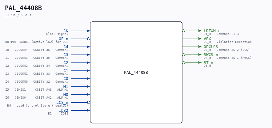
Schematic
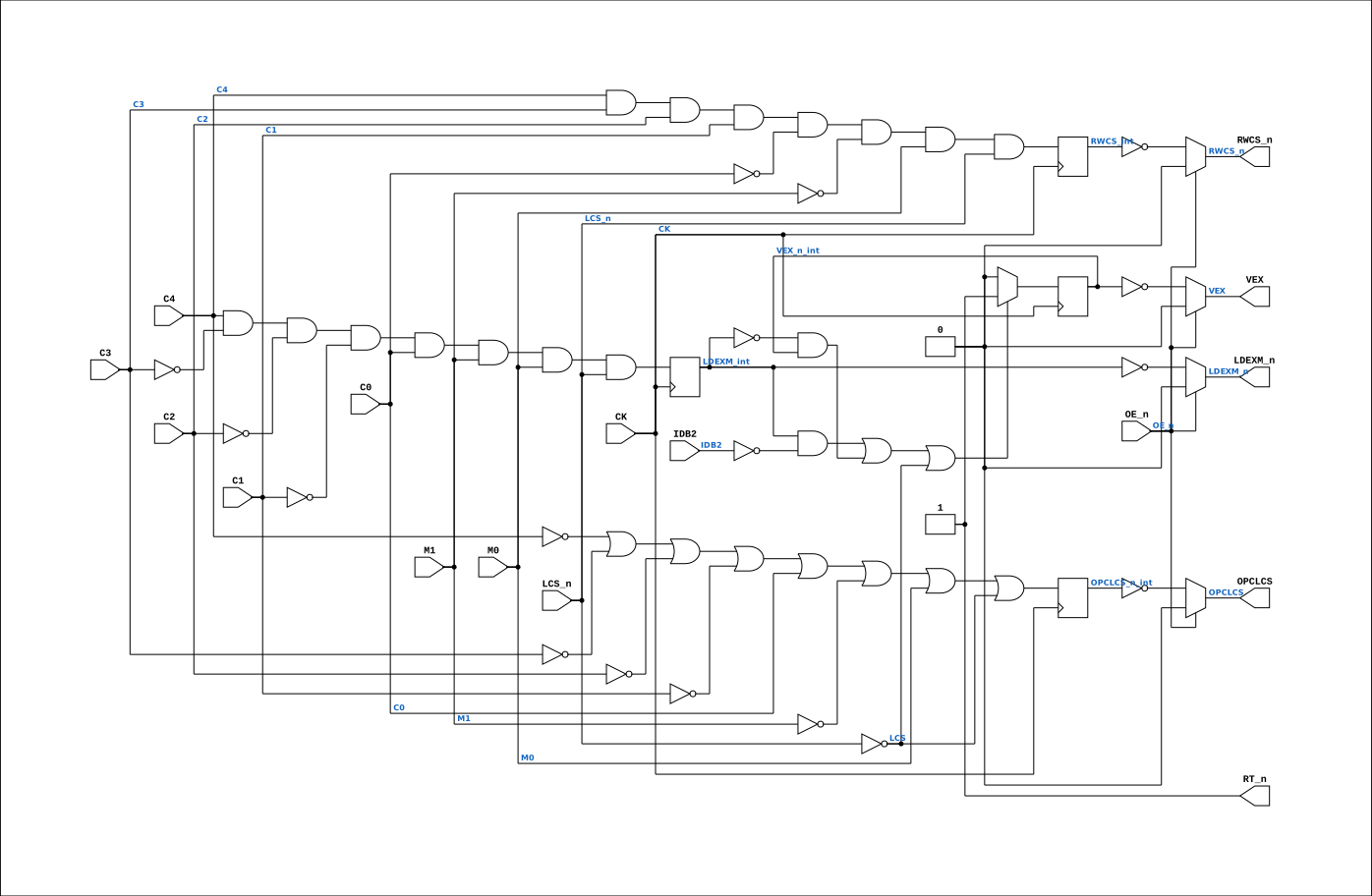
Drawn from the Verilog: no build top uses this module, so it was elaborated from its own file with no defines and default parameters. Sub-modules are boxes (click the picture to open it full size; there every sub-module box links to its page, and every wire shows its Verilog name).
Description
ND120 PALASM CODE CONVERTED TO VERILOG Component PAL 44608A Last reviewed: 19-JAN-2025 Ronny Hansen
Ports
| Direction | Width | Name | Description |
|---|---|---|---|
| input | 1 |
CK |
Clock signal |
| input | 1 |
OE_n (active low) |
OUTPUT ENABLE (active-low) for Q0-Q3 |
| input | 1 |
C4 |
I0 - CSCOMM4 - CSBIT# 36 - Command bit 4 |
| input | 1 |
C3 |
I1 - CSCOMM3 - CSBIT# 35 - Command bit 3 |
| input | 1 |
C2 |
I2 - CSCOMM2 - CSBIT# 34 - Command bit 2 |
| input | 1 |
C1 |
I3 - CSCOMM1 - CSBIT# 33 - Command bit 1 |
| input | 1 |
C0 |
I4 - CSCOMM0 - CSBIT# 32 - Command bit 0 |
| input | 1 |
M1 |
I5 - CSMIS1 - CSBIT #43 - ALU MIS1 SIGNAL (also used for sub-commands for CSCOMM) |
| input | 1 |
M0 |
I6 - CSMIS0 - CSBIT #42 - ALU MIS0 SIGNAL (also used for sub-commands for CSCOMM) |
| input | 1 |
LCS_n (active low) |
B0 - Load Control Store (negated) |
| input | 1 |
IDB2 |
B1_n - IDB2 |
| output | 1 |
LDEXM_n (active low) |
Q1_n - Command 21.3 |
| output | 1 |
VEX |
Q2_n - Violation Exception |
| output | 1 |
OPCLCS |
Q3_n - Command 36.2 (LCS) |
| output | 1 |
RWCS_n (active low) |
Q4_n - Command 36.1 (RWCS) |
| output | 1 |
RT_n (active low) |
Q5_n |
Verilog source
Verilog/PAL/PAL_44408B.v on GitHub.
Show the Verilog of PAL_44408B (124 lines)
/**********************************************************************************************************
** ND120 PALASM CODE CONVERTED TO VERILOG                                                                **
**                                                                                                       **
** Component PAL 44608A                                                                                  **
**                                                                                                       **
** Last reviewed: 19-JAN-2025                                                                            **
** Ronny Hansen                                                                                          **
**
***********************************************************************************************************/

// PAL16R4
// JLB/CJTC 17MAR87
// 44408B,22F,VEXFIX


// PCB 3202D sheet 34:
//
// PAL input signal PD1 is connected to PAL OE_n (and PD1 to PD4 is ALWAYS 0/FALSE in the 3202 circuit board)
//     input signal CLK is connectec to PAL CK pin


/*
; TO FIX VIRTUAL EXAMINE BUG IN CGA
; + MISC. OTHER BUGS.

PAL 44608A (VXFIX) replaces this PAL. The new PAL 44608A is an PAL16R6 that has a pin RT_n output. Use RT_n signal from DGA until we find out what the 44608A does with this signal.
*/

module PAL_44408B (
    input CK,   //! Clock signal
    input OE_n, //! OUTPUT ENABLE (active-low) for Q0-Q3

    input C4,     //! I0 - CSCOMM4 - CSBIT# 36 - Command bit 4
    input C3,     //! I1 - CSCOMM3 - CSBIT# 35 - Command bit 3
    input C2,     //! I2 - CSCOMM2 - CSBIT# 34 - Command bit 2
    input C1,     //! I3 - CSCOMM1 - CSBIT# 33 - Command bit 1
    input C0,     //! I4 - CSCOMM0 - CSBIT# 32 - Command bit 0
    input M1,     //! I5 - CSMIS1   - CSBIT #43 - ALU MIS1 SIGNAL (also used for sub-commands for CSCOMM)
    input M0,     //! I6 - CSMIS0   - CSBIT #42 - ALU MIS0 SIGNAL (also used for sub-commands for CSCOMM)
                  //! I7 - (not connected)
    input LCS_n,  //! B0 - Load Control Store (negated)
    // B0_n - (not connected)
    input IDB2,   //! B1_n - IDB2

    // These signals may have wrong Q pin description, as this is taken from the description of the PAL 444608 (VXFIX) which is a PAL16R6

    // Q0_n - (not connected)
    output LDEXM_n,  //! Q1_n - Command 21.3
    output VEX,      //! Q2_n - Violation Exception
    output OPCLCS,   //! Q3_n - Command 36.2 (LCS)
    output RWCS_n,   //! Q4_n - Command 36.1 (RWCS)

    // Pin in 444608 (VXFIX) but not in 44408B
    output RT_n  //! Q5_n


);

  // Inverted input signals
  wire LCS = ~LCS_n;

  // Internal signals for outputs
  reg RWCS_int, OPCLCS_n_int, VEX_n_int, LDEXM_int;

  // Sequential logic triggered on the rising edge of CLK
  always @(posedge CK) begin
    // Logic for LDEXM
    LDEXM_int <= C4 & ~C3 & ~C2 & ~C1 & C0 & M1 & M0 & LCS_n;  // COMMAND 21.3 LDEXM (validated RH) (Load examine mode in MAC function.)

      // VEX Logic
    if ((LDEXM_int && ~IDB2) || (~LDEXM_int && VEX_n_int) || LCS)
    begin
      VEX_n_int <= 1'b1; // Set /VEX to 1
    end else begin
      VEX_n_int <= 1'b0; // Default: Set /VEX to 0
    end

  /*
      if ((LDEXM_int && IDB2n) | (LCS)) begin
          VEX_n_int <= 1'b1; // Clear
      end else if (LDEXM_int) begin
          VEX_n_int <= 1'b0;  // Hold clear
      end
  */
  /*
    // Logic for VEX
    VEX_n_int <= (
        (LDEXM_int & IDB2n) |  // CLEAR
        (~LDEXM_int & VEX_n_int) |  // HOLD CLEAR
        (LCS)  // LCS
    );
    */
    // Logic for OPCLCS
    OPCLCS_n_int <= ~C4 | ~C3 | ~C2 | ~C1 | C0 | ~M1 | M0 | LCS;  // COMMAND 36.2 LCS (validated RH) - Load control store from PROM. and perform a Master Clear

    // Logic for RWCS
    RWCS_int <= C4 & C3 & C2 & C1 & ~C0 & ~M1 & M0 & LCS_n;  // COMMAND 36.1 RWCS(validated RH) - Read/write control store as addressed by ADCS command

  end

  // Tri-state control for outputs
  // High-impedance state when OE_n is high (active-low)

  assign RWCS_n = OE_n ? 1'b0 : ~RWCS_int;
  assign OPCLCS = OE_n ? 1'b0 : ~OPCLCS_n_int;
  assign VEX = OE_n ? 1'b0 : ~VEX_n_int;
  assign LDEXM_n = OE_n ? 1'b0 : ~LDEXM_int;


  // Unknown signal in this PAL, set high
  assign RT_n = 1'b1;

endmodule


/*
DESCRIPTION

; 180587 M3202B
; 150687 RWCS SIGNAL TOO SLOW FROM NEC G.A. MUST BE DONE IN A PAL.
; 010787 REGISTRATION NUMBER CHANGED FROM 44501B

*/