PAL_45009B
Source: Verilog/PAL/PAL_45009B.v
Where it sits (Simulation): ND120_TOP > ND120_CORE > ND3202D > MEM_43 > MEM_ERROR_47 > PAL_45009B
- instance path: CORE.CPU_BOARD.MEM.ERROR.PAL_45009_UERROR
Used in: MEM_ERROR_47 (all tops)
Contains: no other modules.
Module hierarchy - All modules
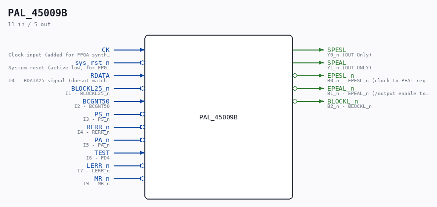
Schematic
Drawn from the Verilog: the yosys netlist of the Simulation (Verilator) build, instance CORE.CPU_BOARD.MEM.ERROR.PAL_45009_UERROR. Sub-modules are boxes (click the picture to open it full size; there every sub-module box links to its page, and every wire shows its Verilog name).
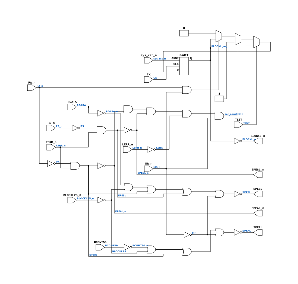
Description
ND120 PALASM CODE CONVERTED TO VERILOG Component PAL 45009B Last reviewed: 2-FEB-2025 Ronny Hansen
Ports
| Direction | Width | Name | Description |
|---|---|---|---|
| input | 1 |
CK |
Clock input (added for FPGA synthesis) |
| input | 1 |
sys_rst_n (active low) |
System reset (active low, for FPGA synthesis) |
| input | 1 |
RDATA |
I0 - RDATA25 signal (doesnt match name) |
| input | 1 |
BLOCKL25_n (active low) |
I1 - BLOCKL25_n |
| input | 1 |
BCGNT50 |
I2 - BCGNT50 |
| input | 1 |
PS_n (active low) |
I3 - PS_n |
| input | 1 |
RERR_n (active low) |
I4 - RERR_n |
| input | 1 |
PA_n (active low) |
I5 - PA_n |
| input | 1 |
TEST |
I6 - PD4 |
| input | 1 |
LERR_n (active low) |
I7 - LERR_n |
| input | 1 |
MR_n (active low) |
I9 - MR_n |
| output | 1 |
SPESL |
Y0_n (OUT Only) |
| output | 1 |
SPEAL |
Y1_n (OUT ONLY) |
| output | 1 |
EPESL_n (active low) |
B0_n - EPESL_n (clock to PEAL register) |
| output | 1 |
EPEAL_n (active low) |
B1_n - EPEAL_n (/output enable to PEAL register) |
| output | 1 |
BLOCKL_n (active low) |
B2_n - BLOCKL_n |
Verilog source
Verilog/PAL/PAL_45009B.v on GitHub.
Show the Verilog of PAL_45009B (126 lines)
/**********************************************************************************************************
** ND120 PALASM CODE CONVERTED TO VERILOG                                                                **
**                                                                                                       **
** Component PAL 45009B                                                                                  **
**                                                                                                       **
** Last reviewed: 2-FEB-2025                                                                             **
** Ronny Hansen                                                                                          **
***********************************************************************************************************/


// PAL16L8
// ADGD 12AUG86
// 45009B,4F ,ERROR


// PCB 3202D sheet 47:
//

// PAL 16L8
// 10 INPUT only pins (I0-I9)
// 2 OUT only pins (Y0-Y1) and 6 IN or OUT pins (B0-B5)
//
// PAL16RL8 (https://rocelec.widen.net/view/pdf/c6dwcslffz/VANTS00080-1.pdf)

// NOTE: PAL16L8 is purely combinational in the original hardware.
// Clock input added for FPGA synthesis to eliminate latch inference.

module PAL_45009B (
    input CK,          //! Clock input (added for FPGA synthesis)
    input sys_rst_n,   //! System reset (active low, for FPGA synthesis)

    input RDATA,       //! I0 - RDATA25 signal (doesnt match name)
    input BLOCKL25_n,  //! I1 - BLOCKL25_n
    input BCGNT50,     //! I2 - BCGNT50
    input PS_n,        //! I3 - PS_n
    input RERR_n,      //! I4 - RERR_n
    input PA_n,        //! I5 - PA_n
    input TEST,        //! I6 - PD4
    input LERR_n,      //! I7 - LERR_n
    // input not_connected,   //! I8 -
    input MR_n,        //! I9 - MR_n


    output SPESL,  //! Y0_n (OUT Only)
    output SPEAL,  //! Y1_n (OUT ONLY)

    output EPESL_n,  //! B0_n - EPESL_n (clock to PEAL register)
    output EPEAL_n,  //! B1_n - EPEAL_n (/output enable to PEAL register)
    output BLOCKL_n  //! B2_n - BLOCKL_n
    // inout B3_n,   //! B3_n - (n.c)
    // inout B4_n,   //! B4_n - (n.c)
    // inout B5_n    //! B5_n - (n.c)
);


  // Verilog code equivalent to the provided PALASM code
  wire RDATA_n = ~RDATA;
  wire BCGNT50_n = ~BCGNT50;
  wire PS = ~PS_n;
  wire PA = ~PA_n;
  wire LERR = ~LERR_n;
  wire MR = ~MR_n;
  wire BLOCKL25 = ~BLOCKL25_n;
  wire EPESL = ~EPESL_n;
  wire EPEAL = ~EPEAL_n;

  reg  BLOCKL_reg;

  //** IGNORING TEST MODE FOR NOW **//

  // RDATA USED AS WRITE PULSE WHEN NOT BLOCKED
  assign SPESL   = ~(RDATA_n | BLOCKL25 | EPEAL | EPESL | MR);

  // BCGNT USED AS WRITE PULSE
  assign SPEAL   = ~(BCGNT50_n | BLOCKL25 | EPEAL | MR);

  // ENABLE IF ERROR IN LOCAL MEMORY
  assign EPESL_n = ~(PS & RERR_n);
  assign EPEAL_n = ~(PA & RERR_n);

  // BLOCKL condition
  wire set_condition = (RDATA & EPEAL_n & EPESL_n & LERR & MR_n);
  wire reset_condition = !(PA_n & MR_n);

`ifdef USE_TRANSPARENT_LATCHES
  // Transparent latch (original behavior for simulation)
  /* verilator lint_off LATCH */
  always @(*) begin
    if (!TEST) begin
      if (set_condition) BLOCKL_reg = 1'b1;  // SET ON LOCAL ERROR
      else if (reset_condition)
        BLOCKL_reg = 1'b0;  // HOLD TILL PEA READ
    end
  end
  /* verilator lint_on LATCH */
`else
  // Edge-triggered flip-flop (FPGA synthesis)
  always @(posedge CK or negedge sys_rst_n) begin
    if (!sys_rst_n) begin
      BLOCKL_reg <= 1'b0;
    end else if (!TEST) begin
      if (set_condition) BLOCKL_reg <= 1'b1;
      else if (reset_condition)
        BLOCKL_reg <= 1'b0;
    end
  end
`endif

  assign BLOCKL_n = ~BLOCKL_reg;

endmodule

/*


DESCRIPTION

; 2/4-87JLB: RDATA PIN 1.
; 070487 JLB: MUST NOT LOCK ON MOR, THAT IS DONE IN THE BUS INTERFACE ANYWAY
; UNBLOCK ON PA (I.E. ALSO IF THE BUS PEA WAS READ)
; 150487 CJTC: NO!!! SPIKES ON SPEAL - USE BLOCKL25 INSTEAD OF BLOCKL
;
; 180587 : M3202B
; 090887 B JLB: TEST MODE FOR C-PRINT.

*/