PAL_44401B
Source: Verilog/PAL/PAL_44401B.v
Where it sits (Simulation): ND120_TOP > ND120_CORE > ND3202D > BIF_5 > BIF_BCTL_6 > PAL_44401B
- instance path: CORE.CPU_BOARD.BIF.BCTL.PAL_44401_UBTIM
Used in: BIF_BCTL_6 (all tops)
Contains: no other modules.
Module hierarchy - All modules
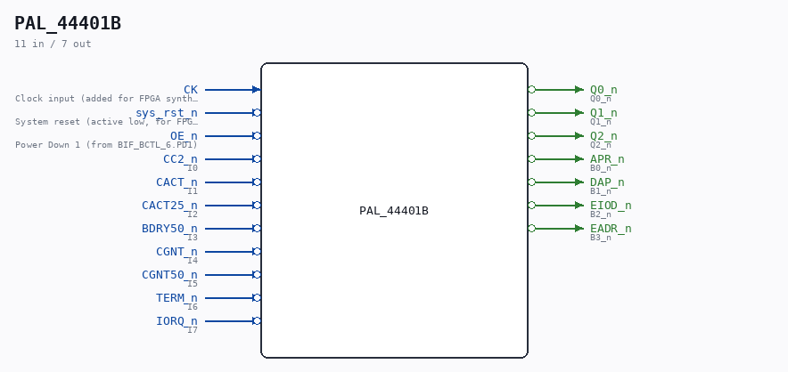
Schematic
Drawn from the Verilog: the yosys netlist of the Simulation (Verilator) build, instance CORE.CPU_BOARD.BIF.BCTL.PAL_44401_UBTIM. Sub-modules are boxes (click the picture to open it full size; there every sub-module box links to its page, and every wire shows its Verilog name).
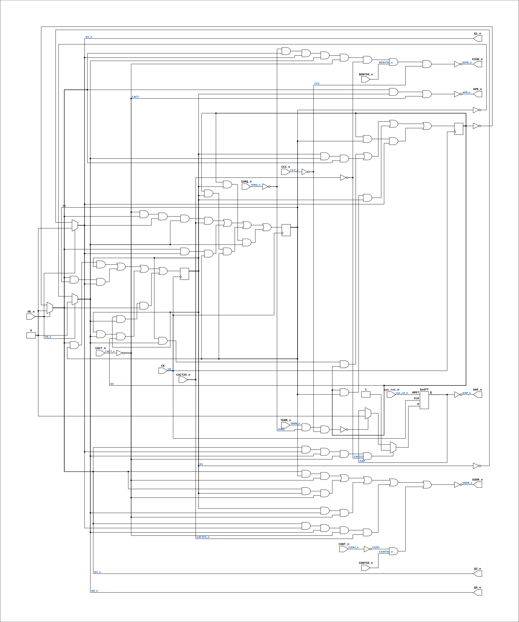
Description
ND120 PALASM CODE CONVERTED TO VERILOG Component PAL 44401B Last reviewed: 2-FEB-2025 Ronny Hansen
Ports
| Direction | Width | Name | Description |
|---|---|---|---|
| input | 1 |
CK |
Clock input (added for FPGA synthesis) (same net as BIF_DPATH_9.OSC) |
| input | 1 |
sys_rst_n (active low) |
System reset (active low, for FPGA synthesis) |
| input | 1 |
OE_n (active low) |
Power Down 1 (from BIF_BCTL_6.PD1) |
| input | 1 |
CC2_n (active low) |
I0 |
| input | 1 |
CACT_n (active low) |
I1 |
| input | 1 |
CACT25_n (active low) |
I2 |
| input | 1 |
BDRY50_n (active low) |
I3 |
| input | 1 |
CGNT_n (active low) |
I4 |
| input | 1 |
CGNT50_n (active low) |
I5 |
| input | 1 |
TERM_n (active low) |
I6 |
| input | 1 |
IORQ_n (active low) |
I7 |
| output | 1 |
Q0_n (active low) |
Q0_n |
| output | 1 |
Q1_n (active low) |
Q1_n |
| output | 1 |
Q2_n (active low) |
Q2_n |
| output | 1 |
APR_n (active low) |
B0_n |
| output | 1 |
DAP_n (active low) |
B1_n |
| output | 1 |
EIOD_n (active low) |
B2_n |
| output | 1 |
EADR_n (active low) |
B3_n |
Verilog source
Verilog/PAL/PAL_44401B.v on GitHub.
Show the Verilog of PAL_44401B (175 lines)
/**********************************************************************************************************
** ND120 PALASM CODE CONVERTED TO VERILOG                                                                **
**                                                                                                       **
** Component PAL 44401B                                                                                  **
**                                                                                                       **
** Last reviewed: 2-FEB-2025                                                                             **
** Ronny Hansen                                                                                          **
***********************************************************************************************************/


// 44401B,5D,BTIM
// PAL16R4D (https://rocelec.widen.net/view/pdf/c6dwcslffz/VANTS00080-1.pdf)


// PCB 3202D sheet 6:
//
// PAL input signal PD1 is connected to PAL OE_n (and PD1 to PD4 is ALWAYS 0/FALSE in the 3202 circuit board)
//     input signal OSC is connectec to PAL CK pin

// I/O 1,2,7, and 8 is not controlled by OE_n

// Four D flip-flops controleed by CLK signal (and reads input to O3,O4,O5 and O6) when transision from LOW to HIGH.
// O3-O6 output is controlled by OE_n (HIGH signal means output is three-state)

module PAL_44401B(
    input CK,           //! Clock input (added for FPGA synthesis) (same net as BIF_DPATH_9.OSC)
    input sys_rst_n, //! System reset (active low, for FPGA synthesis)
    input OE_n,         //! Power Down 1 (from BIF_BCTL_6.PD1)

    input CC2_n,        // I0
    input CACT_n,       // I1
    input CACT25_n,     // I2
    input BDRY50_n,     // I3
    input CGNT_n,       // I4
    input CGNT50_n,     // I5
    input TERM_n,       // I6
    input IORQ_n,       // I7


    output Q0_n,        // Q0_n
    output Q1_n,        // Q1_n
    output Q2_n,        // Q2_n
                        // Q3_n (not connected, no signal)

    output APR_n,       // B0_n
    output DAP_n,       // B1_n
    output EIOD_n,      // B2_n
    output EADR_n       // B3_n
);

// Creating non-negated wires for active-low inputs
wire CC2 = ~CC2_n;
wire CACT = ~CACT_n;
wire CACT25 = ~CACT25_n;
wire CGNT = ~CGNT_n;
wire IORQ = ~IORQ_n;


// Temporary removed because of "unused" warning.
// Which is related to " Feedback to public clock or circular logic: 'DAP_n'"
//wire DAP = ~DAP_n;


// Logic for Q0, Q1, Q2
reg Q0, Q1, Q2;


// Flip-flop logic for Q0, Q1, Q2
always @(posedge CK) begin
    Q0 <=
                    (CACT & Q2_n & Q1_n & Q0_n & CACT25_n) |
                    (Q2_n & Q1_n & Q0)                     |
                    (Q2 & Q1 & Q0)                         |
                    (Q2 & Q1 & Q0_n);


    Q1 <=
                    (Q2_n & Q0 & Q1)   |
                    (Q2_n & Q0 & Q1_n) |
                    (Q1 & Q0_n & Q2)   |
                    (Q1 & Q0_n & Q2_n);


    Q2 <=
                    (Q1 & Q0_n & Q2)   |
                    (Q1 & Q0_n & Q2_n) |
                    (Q2 & Q0 & Q1)     |
                    (Q2 & Q0 & Q1_n);
end


// Output logic for Q0_n, Q1_n, Q2_n
assign Q0_n = OE_n ? 1'b0 : ~Q0;
assign Q1_n = OE_n ? 1'b0 : ~Q1;
assign Q2_n = OE_n ? 1'b0 : ~Q2;


// Logic for APR
assign APR_n = ~(Q2_n & Q1 & CACT);

// Logic for EADR_n (active-low)
assign EADR_n = ~(
                  (Q2_n & Q0 & CACT)                     |   // t + u
                  (Q2_n & Q1 & CACT)                     |   // u + v
                  (Q1 & Q0_n & CACT)                     |   // v + w
                  (Q2_n & Q1_n & Q0_n & CACT & CACT25_n) |   // s
                  (CGNT & CGNT50_n));                        // address part for CPU cycle

// Logic for DAP
reg DAP;

`ifdef USE_TRANSPARENT_LATCHES
// Transparent latch (original behavior for simulation)
/* verilator lint_off LATCH */
always @(*)
begin
    if (Q2_n & Q1_n & Q0_n & CACT & CACT25)
        DAP = 1'b1;
    else if  ((TERM_n & IORQ & CC2) == 0)
        DAP = 1'b0;
end
/* verilator lint_on LATCH */
`else
// Edge-triggered flip-flop (FPGA synthesis)
always @(posedge CK or negedge sys_rst_n)
begin
    if (!sys_rst_n)
        DAP <= 1'b0;
    else if (Q2_n & Q1_n & Q0_n & CACT & CACT25)
        DAP <= 1'b1;
    else if  ((TERM_n & IORQ & CC2) == 0)
        DAP <= 1'b0;
end
`endif

assign DAP_n  = ~DAP;

// Logic for EIOD_n (active-low)
assign EIOD_n = ~(IORQ & Q2_n & Q1_n & Q0_n & CACT & CACT25 & BDRY50_n & CC2);
// STARTS WHEN THE s STATE HAS BEEN REACHED AFTER COMPLETING THE LOOP.

endmodule

/*
DESCRIPTION


;                        |<----------------------------------------------------|
;                                                                              |
;                ------<(s)000                                                 |
;               |     /                                                        |
; /CACT+CACT25  |    /   |                                                     |
;               |   /    |                                                     |
;                --/     |                                                     |
;                        |                                                     |
;                                                                              |
;                        (t)001                                                |
;                                                                              |
;                        |-----(u)-----(v)-----(w)-----(x)-----(y)-----(z)---->|
;                             O11     010     110     111     101     100

; 010387 JLB: EIOD TOO SOON, ONLY 15NS SETUP FOR BD BEFORE BIOXE.
; WOULD NOT LOAD FROM FLOPPY. EIOD FRONT FLANK DELAYED 25NS.

: SAME WITH DAP. DAP HELD FOR THE REST OF THE CYCLE UNTIL TERM
; ON IORQ.
; 060387 JLB: DAP HELD INTO ADDRESS PART OF IOX CYCLES AFTER A
; BUFFERED WRITE CYCLE. SWAPPED IOD FOR IORQ IN EIOD.
; USING CC2 (NEW INPUT) TO QUALIFY DAP AND EIOD
; STATE MACHINE
;
; 180587 M3202B
; 090887 B JLB: MAXIMIZED EQUATIONS TO MATCH CLOCK SKEW.

*/