PAL_44511A
Source: Verilog/PAL/PAL_44511A.v
Hierarchy: not instantiated by any of the 9 build tops (elaborated by yosys).
Module hierarchy - All modules
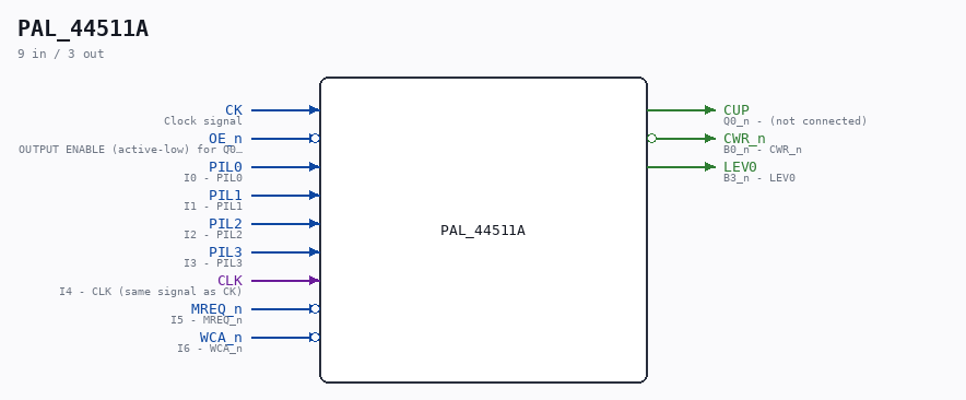
Schematic
Drawn from the Verilog: no build top uses this module, so it was elaborated from its own file with no defines and default parameters. Sub-modules are boxes (click the picture to open it full size; there every sub-module box links to its page, and every wire shows its Verilog name).
Description
ND120 PALASM CODE CONVERTED TO VERILOG Component PAL 44511A Last reviewed: 2-FEB-2025 Ronny Hansen
Ports
| Direction | Width | Name | Description |
|---|---|---|---|
| input | 1 |
CK |
Clock signal |
| input | 1 |
OE_n (active low) |
OUTPUT ENABLE (active-low) for Q0-Q3 |
| input | 1 |
PIL0 |
I0 - PIL0 |
| input | 1 |
PIL1 |
I1 - PIL1 |
| input | 1 |
PIL2 |
I2 - PIL2 |
| input | 1 |
PIL3 |
I3 - PIL3 |
| input | 1 |
CLK |
I4 - CLK (same signal as CK) |
| input | 1 |
MREQ_n (active low) |
I5 - MREQ_n |
| input | 1 |
WCA_n (active low) |
I6 - WCA_n |
| output | 1 |
CUP |
Q0_n - (not connected) |
| output | 1 |
CWR_n (active low) |
B0_n - CWR_n |
| output | 1 |
LEV0 |
B3_n - LEV0 |
Verilog source
Verilog/PAL/PAL_44511A.v on GitHub.
Show the Verilog of PAL_44511A (175 lines)
/**********************************************************************************************************
** ND120 PALASM CODE CONVERTED TO VERILOG                                                                **
**                                                                                                       **
** Component PAL 44511A                                                                                  **
**                                                                                                       **
** Last reviewed: 2-FEB-2025                                                                             **
** Ronny Hansen                                                                                          **
***********************************************************************************************************/


// PAL16R4
// CJTC 30SEP87
// 44511A, 26H, LEV0

// PAL16R4 (https://rocelec.widen.net/view/pdf/c6dwcslffz/VANTS00080-1.pdf)

// Four D flip-flops controlled by CLK signal (and reads input to flip-flop O3,O4,O5 and O6) when transision from LOW to HIGH.
// O3-O6 output is controlled by OE_n (HIGH signal means output is three-state)

// PCB 3202D sheet 34:
//
// PAL input signal PD1 is connected to PAL OE_n (and PD1 to PD4 is ALWAYS 0/FALSE in the 3202 circuit board)
//     input signal CLK is connectec to PAL CK pin


module PAL_44511A (
    input CK,   //! Clock signal
    input OE_n, //! OUTPUT ENABLE (active-low) for Q0-Q3

    input PIL0,    //! I0 - PIL0
    input PIL1,    //! I1 - PIL1
    input PIL2,    //! I2 - PIL2
    input PIL3,    //! I3 - PIL3
    input CLK,     //! I4 - CLK (same signal as CK)
    input MREQ_n,  //! I5 - MREQ_n
    input WCA_n,   //! I6 - WCA_n
    //input I7,       //! I7 - (not connected)

    output CUP,  //! Q0_n - (not connected)
    //output Q1_n,   //! Q1_n - (not connected)
    //output Q2_n,   //! Q2_n - (not connected)
    //output Q2_n,   //! Q3_n - (not connected)


    output CWR_n,  //! B0_n - CWR_n
    //output B1_n,   //! B1_n - (not connected)
    //output B2_n,   //! B2_n - (not connected)
    output LEV0    //! B3_n - LEV0

);


  // Register declarations for state-holding variables
  reg  CWR_hold;
  reg  CUP_n_reg;


  // negated wires
  wire MREQ = ~MREQ_n;
  wire WCA = ~WCA_n;
  wire CLK_n = ~CLK;

  // CWR IS COMBINATIONAL, NOT REGISTERED. From the original PALASM,
  // DesignDocuments/PAL-Code/SRC/44511A.txt:
  //
  //   IF (VCC) CWR  = MREQ * WCA + CWR * /CLK    <-- '='  combinational
  //           /CUP := /CWR * MREQ + /CUP * /MREQ <-- ':=' registered
  //
  // In PALASM '=' is a combinational output and ':=' a registered one, and
  // on a PAL16R4 only Q0-Q3 have flip-flops - CWR is pin B0, which has
  // none. LEV0 (B3) in this same file was already modelled combinationally;
  // CWR was not, and that was the bug.
  //
  // WHY IT MATTERED. A registered CWR is not visible until the NEXT clock
  // edge, by which time MREQ has gone. The CUP term /CWR * MREQ needs both
  // in the SAME cycle, so CUP never asserted at all. Everything followed
  // from that: the used-bit PAL never wrote, CHIP_21F stayed zero, and
  // s_hit - which requires !s_used_n - could never assert. The machine's
  // own diagnostic (CACHE-120-A00 under TPE) reported exactly that chain:
  // "CUP does not work", "DATA is NOT COPIED to DATA CACHE", used bit
  // "Expected 1 Found 0", while the cache DATA memory test passed.
  //
  // HOW IT IS MODELLED HERE (FF mode, chosen 28-AUG-2026). The set term is
  // combinational, so CWR is visible in the very cycle MREQ * WCA happens -
  // that is what CUP needs. The hold term is a register qualified by /CLK,
  // matching "HOLD UNTIL START OF NEXT CYCLE": the hold dies at the CLK rise,
  // so CWR does not survive into the high phase.
  //
  // RESIDUAL DEVIATION, stated plainly. The real pin is a LEVEL-sensitive
  // feedback latch that sets the instant MREQ * WCA occurs during the low
  // phase. A flop clocked at the CLK rise cannot see inside that phase, so the
  // hold here is one CLK rise behind: an event captured at a rise can extend
  // CWR across the FOLLOWING low phase, which the PAL would not do. The set
  // term is unaffected, and it is the set term CUP samples. This is the
  // USE_LATCHES=0 path the FPGA builds; do not "fix" it by inferring a latch
  // without going through the repo's latch-vs-FF compare first.
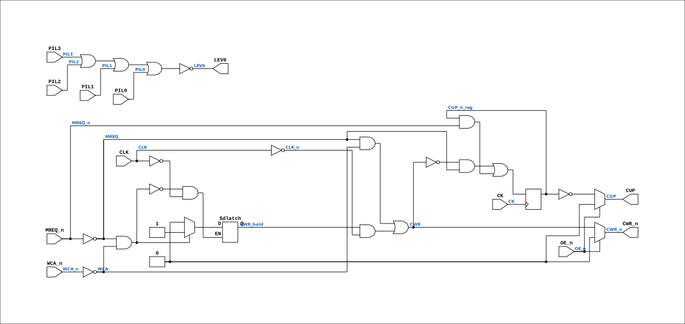
  wire CWR = (MREQ & WCA) | (CWR_hold & CLK_n);

  // LEVEL ZERO
  assign LEV0 = ~(PIL3 | PIL2 | PIL1 | PIL0);


  // THE HOLD IS A LEVEL LATCH, not a flop (29-AUG-2026). The listing's
  //   CWR = MREQ * WCA + CWR * /CLK
  // is a feedback latch on a combinational pin: it sets the instant
  // MREQ * WCA appears and holds for the rest of the CLK-low phase. Loading
  // the hold on the CK edge (the previous model) only remembered a WCA that
  // was still present AT the edge; on this board WCA lives in cycle state d
  // and CLK rises at TERM, four states later, so every cache write was lost
  // and CACHE-1X0-A00 reported "CUP does not work" (measured in Verilator,
  // runSim ND120_CACHE_TRACE). PAL_44511A_EN.v models the same latch at
  // sysclk rate; keep the two in step.
  always @(*) begin
    if (MREQ & WCA)   CWR_hold = 1'b1;   // set on write to cache
    else if (CLK)     CWR_hold = 1'b0;   // dies once CLK is high
    // else: hold (CLK low, no new write)
  end

  always @(posedge CK) begin

    // Logic for CUP (ADDED CACHE UPDATE BIT). 44511A OCR/PNG (registered):
    //   /CUP := /CWR * MREQ + /CUP * /MREQ
    //   (intent: CUP := CWR*MREQ + CUP*/MREQ - SET on write-to-cache, hold until next MREQ).
    // Fix 26-JUL: the prior if/else had the MREQ polarity flipped (CWR_n & MREQ_n),
    // so CUP was never set on a cache write and spuriously set when idle -> the
    // CACHE-1X0 diagnostic reported "Cache updated bit: Not working".
    CUP_n_reg <= (~CWR & MREQ) | (CUP_n_reg & MREQ_n);
  end

  // PIN 19 POLARITY (29-AUG-2026, 23:30) - THE CACHE'S FAULT 2.
  //
  // MEASURED (runSim, CACHE-1X0-A00 test 2, per-clock log of the test's
  // read of the word it had just written): both tag comparators match,
  // the used bit is set and valid, RT and DT are asserted, no write is
  // in progress - and sheet 25's HIT stays 0 on every clock of the
  // cycle. The only HIT input left is this pin. Same six test-2 lines on
  // the Nexys with everything else fixed, so it is not a model artefact.
  //
  // THE HARDWARE. Sheet 25: HIT is the output of a 74S260 5-input NOR
  // (21H) whose inputs are USED~, HIT~1, HIT~0, the net CWR and ground -
  // HIT is high only when ALL of them are LOW. Sheet 34: net CWR is pin
  // 19 of this PAL, wired straight to the connector, no inverter. So on
  // the real board pin 19 must be LOW on a normal read and go HIGH only
  // across a cache write (MREQ * WCA, held until CLK) - that is the pin
  // FOLLOWING the listing's CWR expression, not its complement.
  //
  // This file used to drive the complement ("/CWR is active low, pin =
  // ~CWR", the convention the 44402D's /USED and /WCA pins follow and
  // which is right for them). For this pin that makes HIT possible only
  // WHILE the cache is being written, i.e. never on a read: every read
  // ran the full memory cycle and took the memory word, exactly the
  // "DATA is taken FROM MEMORY when present in DATA CACHE" family of
  // errors. The listing's naming and the schematic's naming disagree on
  // this net (the listing calls the pin /CWR, both sheets call the net
  // CWR with no ~), and the measurement decides: the pin follows CWR.
  // The CUP equation below uses the internal CWR and is unaffected.
  // outputs
  assign CWR_n = OE_n ? 1'b0 : CWR;   // pin 19 follows CWR - see the note above
  assign CUP   = OE_n ? 1'b0 : ~CUP_n_reg;


endmodule


/*
DESCRIPTION

; 180587 M3202B

061087 CJTC : ADDED CACHE UPDATE BIT (CUP) FOR M3202D

*/