IO_UART_42
Source: Verilog/CPU-BOARD-3202/circuit/IO_UART_42.v
Where it sits (Simulation): ND120_TOP > ND120_CORE > ND3202D > IO_37 > IO_UART_42
- instance path: CORE.CPU_BOARD.IO.UART
Used in: IO_37 (all tops)
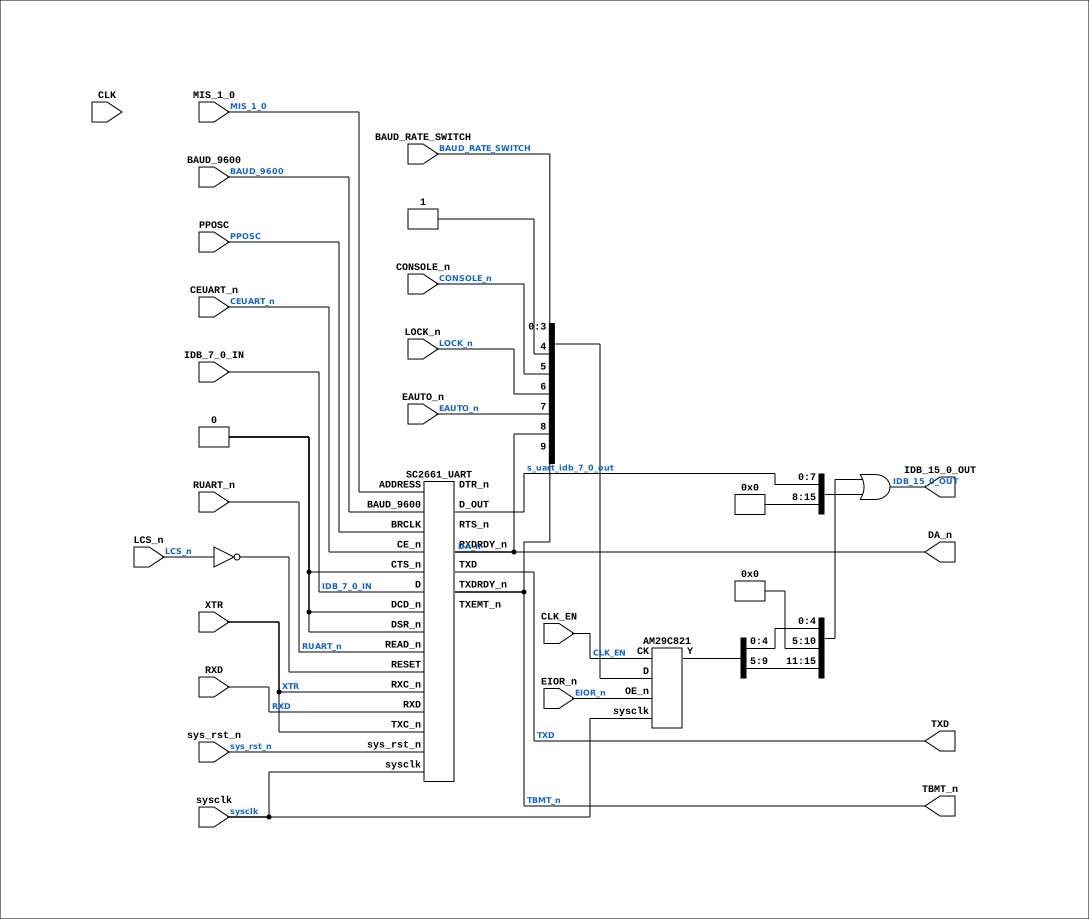
Contains: AM29C821, SC2661_UART
Module hierarchy - All modules
Schematic
Drawn from the Verilog: the yosys netlist of the Simulation (Verilator) build, instance CORE.CPU_BOARD.IO.UART. Sub-modules are boxes (click the picture to open it full size; there every sub-module box links to its page, and every wire shows its Verilog name).
Description
ND120 CPU, MM&M IO/UART UART & IOR REG SHEET 42 of 50 Last reviewed: 14-DEC-2024 Ronny Hansen
Ports
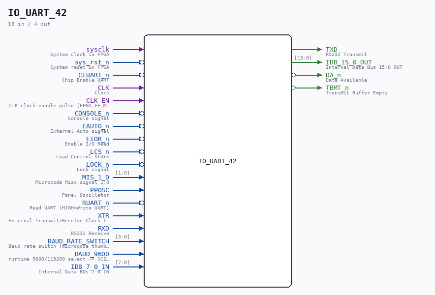
| Direction | Width | Name | Description |
|---|---|---|---|
| input | 1 |
sysclk |
System clock in FPGA |
| input | 1 |
sys_rst_n (active low) |
System reset in FPGA |
| input | 1 |
CEUART_n (active low) |
Chip Enable UART |
| input | 1 |
CLK |
Clock |
| input | 1 |
CLK_EN |
CLK clock-enable pulse (FPGA_FF_MODE, else 0) |
| input | 1 |
CONSOLE_n (active low) |
Console signal |
| input | 1 |
EAUTO_n (active low) |
External Auto signal |
| input | 1 |
EIOR_n (active low) |
Enable I/O Read |
| input | 1 |
LCS_n (active low) |
Load Control Store |
| input | 1 |
LOCK_n (active low) |
Lock signal |
| input | [1:0] |
MIS_1_0 |
Microcode Misc signal 1:0 |
| input | 1 |
PPOSC |
Panel Oscillator |
| input | 1 |
RUART_n (active low) |
Read UART (HIGH=Write UART) |
| input | 1 |
XTR |
External Transmit/Receive Clock (not used) |
| input | 1 |
RXD |
RS232 Receive |
| output | 1 |
TXD |
RS232 Transmit |
| input | [3:0] |
BAUD_RATE_SWITCH |
Baud rate switch (microcode thumbwheel) |
| input | 1 |
BAUD_9600 |
runtime 9600/115200 select -> SC2661 |
| input | [7:0] |
IDB_7_0_IN |
Internal Data Bus 7:0 IN |
| output | [15:0] |
IDB_15_0_OUT |
Internal Data Bus 15:0 OUT |
| output | 1 |
DA_n (active low) |
Data Available |
| output | 1 |
TBMT_n (active low) |
Transmit Buffer Empty |
Verilog source
Verilog/CPU-BOARD-3202/circuit/IO_UART_42.v on GitHub.
Show the Verilog of IO_UART_42 (221 lines)
/**************************************************************************
** ND120 CPU, MM&M                                                       **
** IO/UART                                                               **
** UART & IOR REG                                                        **
** SHEET 42 of 50                                                        **
**                                                                       **
** Last reviewed: 14-DEC-2024                                            **
** Ronny Hansen                                                          **
***************************************************************************/


module IO_UART_42 (
    input sysclk,    //! System clock in FPGA
    input sys_rst_n, //! System reset in FPGA

    // Input signals
    input       CEUART_n,   //! Chip Enable UART
    input       CLK,        //! Clock
    input       CLK_EN,     //! CLK clock-enable pulse (FPGA_FF_MODE, else 0)
    input       CONSOLE_n,  //! Console signal
    input       EAUTO_n,    //! External Auto signal
    input       EIOR_n,     //! Enable I/O Read
    input       LCS_n,      //! Load Control Store
    input       LOCK_n,     //! Lock signal
    input [1:0] MIS_1_0,    //! Microcode Misc signal 1:0
    input       PPOSC,      //! Panel Oscillator
    input       RUART_n,    //! Read UART (HIGH=Write UART)
    input       XTR,        //! External Transmit/Receive Clock (not used)

    // RS232 RX/TX signals
    input  RXD,  //! RS232 Receive
    output TXD,  //! RS232 Transmit

    // Baud rate settings
    input [3:0] BAUD_RATE_SWITCH,  //! Baud rate switch (microcode thumbwheel)
    input BAUD_9600,               //! runtime 9600/115200 select -> SC2661

    // Output and Input signals
    input  [ 7:0] IDB_7_0_IN,   //! Internal Data Bus 7:0 IN
    output [15:0] IDB_15_0_OUT, //! Internal Data Bus 15:0 OUT

    // Output signals
    output DA_n,   //! Data Available
    output TBMT_n  //! Transmit Buffer Empty

);

  /*******************************************************************************
   ** The wires are defined here                                                 **
   *******************************************************************************/
  wire [ 7:0] s_idb_7_0_in;
  wire [ 1:0] s_mis_1_0;

`ifdef ND120_ILA_MARK_DEBUG
  (* mark_debug = "true" *)
`endif
  wire [15:0] s_io_idb_15_0_out;
  wire [ 7:0] s_uart_idb_7_0_out;


  wire        s_ceuart_n;
  wire        s_clk;
  // ND120_ILA_MARK_DEBUG (Nexys build.tcl -tclargs ila): keep the console
  // status-capture nets through synthesis so the JTAG ILA can compare the
  // LIVE TBMT_n against the CHIP_33G-captured IOR bit and see whether the
  // FF-mode CLK_EN capture pulse arrives (LIST-FILE-NAMES never-ready
  // campaign, 24-AUG). No functional effect; define set only by that flag.
`ifdef ND120_ILA_MARK_DEBUG
  (* mark_debug = "true" *)
`endif
  wire        s_clk_en;
  wire        s_console_n;
  wire        s_da_n;
  wire        s_eauto_n;
`ifdef ND120_ILA_MARK_DEBUG
  (* mark_debug = "true" *)
`endif
  wire        s_eiorn_n;
  wire        s_gnd;
  wire        s_lcs_n;
  wire        s_lock_n;
  wire        s_pposc;
  wire        s_ruart_n;
  wire        s_rx;
  wire        s_rxd;
`ifdef ND120_ILA_MARK_DEBUG
  (* mark_debug = "true" *)
`endif
  wire        s_tbmt_n;
  wire        s_txd;
  wire        s_xtr;

  /*******************************************************************************
   ** The module functionality is described here                                 **
   *******************************************************************************/

  /*******************************************************************************
   ** Here all input connections are defined                                     **
   *******************************************************************************/
  assign s_mis_1_0[1:0]          = MIS_1_0;
  assign s_lock_n                = LOCK_n;
  assign s_ceuart_n              = CEUART_n;
  assign s_xtr                   = XTR;
  assign s_console_n             = CONSOLE_n;
  assign s_ruart_n               = RUART_n;
  assign s_pposc                 = PPOSC;
  assign s_eiorn_n               = EIOR_n;
  assign s_clk                   = CLK;
  assign s_clk_en                = CLK_EN;
  assign s_eauto_n               = EAUTO_n;
  assign s_lcs_n                 = LCS_n;
  assign s_rxd                   = RXD;
  assign s_idb_7_0_in            = IDB_7_0_IN;

  /*******************************************************************************
   ** Here all output connections are defined                                    **
   *******************************************************************************/

  assign IDB_15_0_OUT            = s_io_idb_15_0_out[15:0] | {8'b0, s_uart_idb_7_0_out[7:0]};

  assign s_io_idb_15_0_out[10:5] = 6'b0;

  assign TXD                     = s_txd;

  // Both DA and TBMT are pulled high
  // DA_n (or /RXRDY from UART) signal is only valid when the receiver is enabled
  assign DA_n                    = s_da_n;

  // TBMT_n (or /TXRDY from UART) signal is only valid when the transmitter is enabled
  assign TBMT_n                  = s_tbmt_n;


  /*******************************************************************************
   ** Here all in-lined components are defined                                   **
   *******************************************************************************/
  assign s_gnd                   = 1'b0;
  assign s_rx                    = s_rxd;


  // P2 (docs/plan-fix-unconstrained-clocks.md): CHIP_33G is the only flop in
  // this module clocked by the board CLK domain. AM29C821 USE_SYSCLK=1 captures
  // D on posedge sysclk while CK is high, so driving CK with the 1-sysclk-wide
  // CLK_EN pulse (aligned to the CLK rise) gives the exact
  // "posedge sysclk + if (CLK_EN)" capture in the sysclk domain.
`ifdef FPGA_FF_MODE
  localparam CLK_CE = 1;
`else
  localparam CLK_CE = 0;
`endif

  AM29C821 #(.USE_SYSCLK(1)) CHIP_33G (
      .sysclk(sysclk),
      .CK((CLK_CE != 0) ? s_clk_en : s_clk),  // domain CLK -> CLK_EN in FF mode
      .OE_n(s_eiorn_n),
      .D({s_tbmt_n, s_da_n, s_eauto_n, s_lock_n, s_console_n, 1'b1, BAUD_RATE_SWITCH[3:0]}),
      .Y({s_io_idb_15_0_out[15:11], s_io_idb_15_0_out[4:0]})
  );

`ifdef ND120_IOR_PROBE
  // DIAGNOSTIC (IDENT PL10 hunt, 20-AUG-2026): every microcode IDBS,IOR read
  // (EIOR_n low) logs the CAPTURED CHIP_33G bits 15/14 next to the LIVE
  // TBMT_n/DA_n, so a stale FF-mode capture is visible as cap!=live.
  // TBMT_n edges are logged too. Sim-only, no logic effect.
  reg r_iorp_eior_prev, r_iorp_tbmt_prev, r_iorp_da_prev;
  always @(posedge sysclk) begin
    if (!s_eiorn_n && r_iorp_eior_prev)
      $display("[ior] t=%0t READ cap15=%b cap14=%b live_tbmt_n=%b live_da_n=%b",
               $time, s_io_idb_15_0_out[15], s_io_idb_15_0_out[14], s_tbmt_n, s_da_n);
    if (s_tbmt_n != r_iorp_tbmt_prev)
      $display("[ior] t=%0t TBMT_n=%b", $time, s_tbmt_n);
    if (s_da_n != r_iorp_da_prev)
      $display("[ior] t=%0t DA_n=%b", $time, s_da_n);
    r_iorp_eior_prev <= s_eiorn_n;
    r_iorp_tbmt_prev <= s_tbmt_n;
    r_iorp_da_prev   <= s_da_n;
  end
`endif

  SC2661_UART CHIP_32H (
      .sysclk(sysclk),  // System clock in FPGA
      .sys_rst_n(sys_rst_n),  // System reset in FPGA
      .BAUD_9600(BAUD_9600),  // runtime baud select (9600 vs 115200)

      .ADDRESS(s_mis_1_0[1:0]),

      .BRCLK(s_pposc),
      .RESET(!s_lcs_n),

      .CE_n  (s_ceuart_n),
      .READ_n(s_ruart_n),


      .CTS_n(s_gnd),  // always low
      .DCD_n(s_gnd),  // always low
      .DSR_n(s_gnd),  // always low

      /* verilator lint_off PINCONNECTEMPTY */
      .DTR_n(),  // not connected
      .RTS_n(),  // not connected
      /* verilator lint_on PINCONNECTEMPTY */


      .D(s_idb_7_0_in[7:0]),
      .D_OUT(s_uart_idb_7_0_out[7:0]),

      .RXC_n(s_xtr),
      .RXD(s_rx),
      .RXDRDY_n(s_da_n),

      .TXC_n(s_xtr),
      .TXD(s_txd),
      .TXDRDY_n(s_tbmt_n),

      /* verilator lint_off PINCONNECTEMPTY */
      .TXEMT_n()
      /* verilator lint_on PINCONNECTEMPTY */
  );

endmodule