SC2661_UART
Source: Verilog/Shared/support/SC2661_UART.v
Where it sits (Simulation): ND120_TOP > ND120_CORE > ND3202D > IO_37 > IO_UART_42 > SC2661_UART
- instance path: CORE.CPU_BOARD.IO.UART.CHIP_32H
Used in: IO_UART_42 (all tops)
Contains: no other modules.
Module hierarchy - All modules
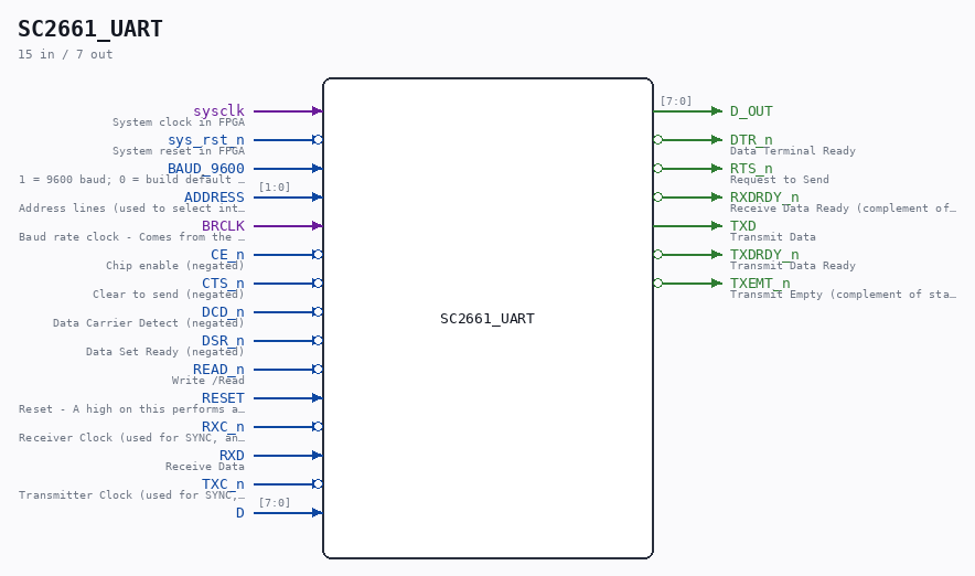
Schematic
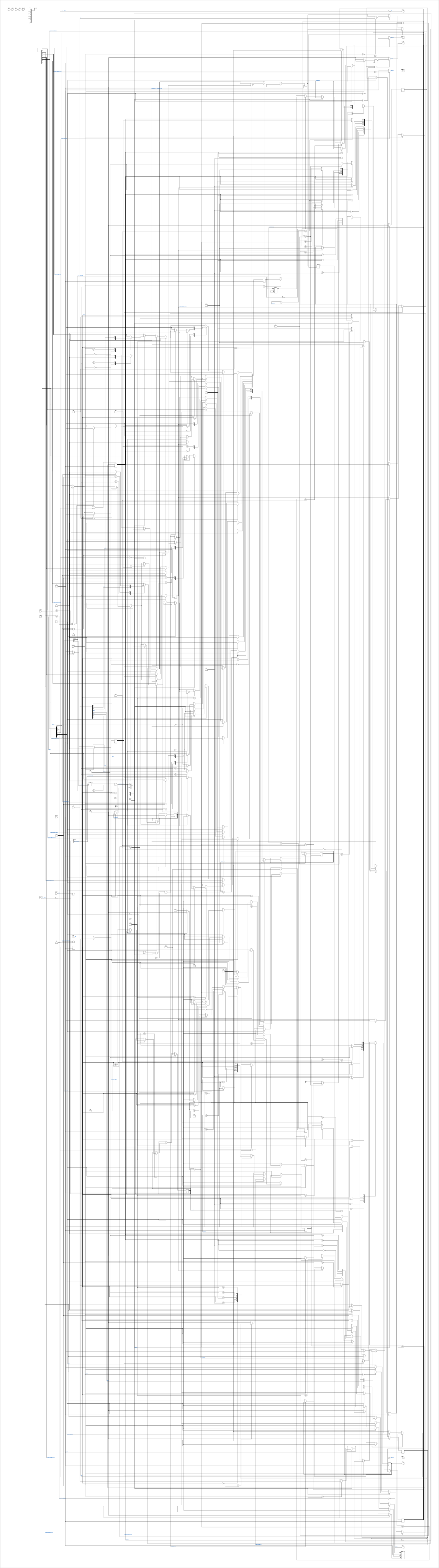
Drawn from the Verilog: the yosys netlist of the Simulation (Verilator) build, instance CORE.CPU_BOARD.IO.UART.CHIP_32H. Sub-modules are boxes (click the picture to open it full size; there every sub-module box links to its page, and every wire shows its Verilog name).
Description
SC2661 UART The SC2661 is a UART (Universal Asynchronous Receiver/Transmitter) chip Last reviewed: 9-FEB-2025 Ronny Hansen
Ports
| Direction | Width | Name | Description |
|---|---|---|---|
| input | 1 |
sysclk |
System clock in FPGA |
| input | 1 |
sys_rst_n (active low) |
System reset in FPGA |
| input | 1 |
BAUD_9600 |
1 = 9600 baud; 0 = build default (UART_BAUD_RATE, normally 115200) - runtime select |
| input | [1:0] |
ADDRESS |
Address lines (used to select internal EPCI registers) |
| input | 1 |
BRCLK |
Baud rate clock - Comes from the IO_DCD module. 4.9152Mhz |
| input | 1 |
CE_n (active low) |
Chip enable (negated) |
| input | 1 |
CTS_n (active low) |
Clear to send (negated) |
| input | 1 |
DCD_n (active low) |
Data Carrier Detect (negated) |
| input | 1 |
DSR_n (active low) |
Data Set Ready (negated) |
| input | 1 |
READ_n (active low) |
Write /Read |
| input | 1 |
RESET |
Reset - A high on this performs a master reset of the chip |
| input | 1 |
RXC_n (active low) |
Receiver Clock (used for SYNC, and not implemented) |
| input | 1 |
RXD |
Receive Data |
| input | 1 |
TXC_n (active low) |
Transmitter Clock (used for SYNC, and not implemented) |
| input | [7:0] |
D |
|
| output | [7:0] |
D_OUT |
|
| output | 1 |
DTR_n (active low) |
Data Terminal Ready |
| output | 1 |
RTS_n (active low) |
Request to Send |
| output | 1 |
RXDRDY_n (active low) |
Receive Data Ready (complement of status register bit SR1) |
| output | 1 |
TXD |
Transmit Data |
| output | 1 |
TXDRDY_n (active low) |
Transmit Data Ready |
| output | 1 |
TXEMT_n (active low) |
Transmit Empty (complement of status register bit SR2) |
Verilog source
Verilog/Shared/support/SC2661_UART.v on GitHub.
Show the Verilog of SC2661_UART (658 lines)
/****************************************************************************
** SC2661 UART **
** **
** The SC2661 is a UART (Universal Asynchronous Receiver/Transmitter) chip **
** **
** Last reviewed: 9-FEB-2025 **
** Ronny Hansen **
*****************************************************************************/
//
// SET YOUR TERMINAL TO 8N1. NOT 7E1.
//
// This implementation is FIXED at 8 data bits, no parity, 1 stop bit. Only the baud rate is
// configurable (BOARD_CLK_FREQ / UART_BAUD_RATE below, default 115200). The real chip's mode
// registers - which is where character length and parity would be selected - are not
// implemented; see the comment where they would have been.
//
// The state machines are the proof, not just that comment: TX_STATE_WRITE shifts out bits 0..7
// and goes straight to TX_STATE_STOP_BIT, RX_STATE_READ shifts in bits 0..7 and goes straight to
// RX_STATE_STOP_BIT. Neither has a parity state, and the word "parity" appears nowhere in this
// file. No parity bit is generated, and none is checked.
//
// WHY THIS WARNING IS HERE, 30-AUG-2026: a PC was set to 7E1 against this UART because the
// datasheet and HARDWARE.md both describe what the REAL chip could be programmed to do. The PC
// then validated a parity bit that is never sent, and the characters it judged bad were replaced
// with '?' scattered through the text - which read like the ND was sending them. An evening went
// into finding that. The full account, with the measurements, is in HARDWARE.md under
// "Serial Interface (UART)".
//
//
// Documentation
//
// http://www.norsk-data.com/hardware/nd-100/nd-350104.html
//
// SCN2661A UART
// http://www.norsk-data.com/library/libother/extern/SCN2661.pdf
//
// Enhanced Programmable Communication Interface EPCI
// https://datasheetspdf.com/pdf-file/1412058/SMSC/COM2661-3/1
//
// Note: Not all functionality is implemented. Just enough to have a simple UART interface for the ND-120 CPU
module SC2661_UART (
input sysclk, // System clock in FPGA
input sys_rst_n, // System reset in FPGA
input BAUD_9600, //! 1 = 9600 baud; 0 = build default (UART_BAUD_RATE, normally 115200) - runtime select
input [1:0] ADDRESS, // Address lines (used to select internal EPCI registers)
input BRCLK, // Baud rate clock - Comes from the IO_DCD module. 4.9152Mhz
input CE_n, // Chip enable (negated)
input CTS_n, // Clear to send (negated)
input DCD_n, // Data Carrier Detect (negated)
input DSR_n, // Data Set Ready (negated)
input READ_n, // Write /Read
input RESET, // Reset - A high on this performs a master reset of the chip
input RXC_n, // Receiver Clock (used for SYNC, and not implemented)
input RXD, // Receive Data
input TXC_n, // Transmitter Clock (used for SYNC, and not implemented)
input [7:0] D,
output [7:0] D_OUT,
output DTR_n, // Data Terminal Ready
output RTS_n, // Request to Send
output RXDRDY_n, // Receive Data Ready (complement of status register bit SR1)
output TXD, // Transmit Data
output TXDRDY_n, // Transmit Data Ready
output TXEMT_n // Transmit Empty (complement of status register bit SR2)
);
/*******************************************************************************
** The wires are defined here **
*******************************************************************************/
/* verilator lint_off UNUSEDSIGNAL */
wire s_brkclk;
wire s_txc_n;
wire s_rxc_n;
wire s_cts_n;
/* verilator lint_on UNUSEDSIGNAL */
wire s_ce_n;
wire s_dcd_n;
wire s_dsr_n;
wire s_dtr_n;
wire s_read_n;
wire s_reset;
wire s_rts_n;
wire s_rxd;
wire s_rxrdy_n;
wire s_txd;
wire s_txemt_n;
wire s_txrdy_n;
wire [1:0] s_address;
wire [7:0] s_data_in;
/*******************************************************************************
** Command register bits **
*******************************************************************************/
wire cmd_txEnabled;
wire cmd_forceDTRLow;
wire cmd_rxEnabled;
/* verilator lint_off UNUSEDSIGNAL */
wire cmd_CR3; // ASYNC: 0=Normal, 1=Force Break. SYNC: 0=Normal, 1=Send DLE (not implemented)
/* verilator lint_on UNUSEDSIGNAL */
wire cmd_resetError;
wire cmd_forceRTSLow;
wire [1:0] cmd_OperatingMode;
//localparam cmd_OperatingMode_NORMAL = 2'b00; // not used..in code.. yet
//localparam cmd_OperatingMode_ASYNC = 2'b01; // not used..in code.. yet
localparam cmd_OperatingMode_LocalLoopback = 2'b10;
localparam cmd_OperatingMode_RemoteLoopback = 2'b11;
/*******************************************************************************
** Mode register 1 and 2 bits **
*******************************************************************************/
// Not implemented, we use constant 9600 8N1, or later 115200 8N1
/*******************************************************************************
** State machine for the receiver and transmitter **
*******************************************************************************/
localparam RX_STATE_IDLE = 3'b000; // 0
localparam RX_STATE_START_BIT = 3'b001; // 1
localparam RX_STATE_READ_WAIT = 3'b010; // 2
localparam RX_STATE_READ = 3'b011; // 3
localparam RX_STATE_STOP_BIT = 3'b101; // 4
localparam RX_STATE_DONE = 3'b110; // 5
localparam TX_STATE_IDLE = 3'b000; // 0
localparam TX_STATE_START_BIT = 3'b001; // 1
localparam TX_STATE_WRITE = 3'b010; // 2
localparam TX_STATE_STOP_BIT = 3'b011; // 3
localparam TX_STATE_DONE = 3'b100; // 4
// Baud rate timing: DELAY_FRAMES = clock cycles per bit
// Set via defines in Makefile/project:
// -DBOARD_CLK_FREQ=100000000 -DUART_BAUD_RATE=115200
//
// Examples:
// 100 MHz / 115200 = 868 (Basys3/Arty)
// 27 MHz / 115200 = 234 (Tang Nano 9K/20K)
// 50 MHz / 115200 = 434 (50 MHz board)
`ifndef BOARD_CLK_FREQ
`define BOARD_CLK_FREQ 100_000_000 // Default: 100 MHz (Basys3/Arty)
`endif
`ifndef UART_BAUD_RATE
`define UART_BAUD_RATE 115_200 // Default: 115200 baud
`endif
`ifdef ND120_UART_DELAY_FRAMES
// Explicit override: real-timing UART in simulation. Set to the silicon
// clocks-per-bit ratio (Nexys 16.67 MHz / 9600 = 1736) to reproduce
// polling-loop pacing that the fast sim UART hides - the FILSYS
// "DEVICE NEVER READY" retry path is only reachable when the TX-ready
// poll actually spins (24-AUG LIST-FILE-NAMES campaign).
localparam DELAY_DEFAULT = `ND120_UART_DELAY_FRAMES;
`elsif VERILATOR_SIM
localparam DELAY_DEFAULT = 32'd16; // Fast for simulation
`else
localparam DELAY_DEFAULT = `BOARD_CLK_FREQ / `UART_BAUD_RATE;
`endif
`ifdef VERILATOR_SIM
localparam DELAY_9600 = 32'd16; // keep sim fast regardless of the switch
`else
localparam DELAY_9600 = `BOARD_CLK_FREQ / 9600;
`endif
//! Runtime baud select (BAUD_9600 input). High -> 9600, low -> the build
//! default (UART_BAUD_RATE, normally 115200). A board switch can drop the
//! console to 9600 for software that cannot take 115200, with no rebuild.
//! The microcode baud thumbwheel is unaffected - only this divisor changes.
wire [31:0] DELAY_FRAMES = BAUD_9600 ? DELAY_9600[31:0] : DELAY_DEFAULT[31:0];
wire [31:0] HALF_DELAY_WAIT = (DELAY_FRAMES >> 1);
// Chip Registers
reg [ 7:0] regDataOut;
reg [ 7:0] regTransmitHoldingRegister;
reg [ 7:0] regStatusRegister;
reg [ 7:0] regModeRegister;
reg [ 7:0] regCommandRegister;
// Transmitter local variables
reg [ 2:0] txState;
reg [31:0] txCounter;
reg [ 2:0] txBitNumber;
reg txBit;
reg regDataInSendRegister; // 1=Data in send register (=>TxEmpty =0)
// Receiver local variables
reg [ 2:0] rxState = 0;
reg [31:0] rxCounter = 0;
reg [ 2:0] rxBitNumber = 0;
//! Live shift-in register for the byte currently arriving. Separate from
//! the RX FIFO below on purpose - see the overrun fix note at the
//! receiver state machine below (31-AUG-2026).
reg [ 7:0] regRxShift = 0;
//! 16-byte RX FIFO between the receiver and the CPU-visible read port
//! (added 31-AUG-2026, after the atomic-transfer fix above). The real
//! 2661 holds exactly one received byte - no queue - and until now this
//! model matched that. But a TDV2200 keyboard escape sequence can be up
//! to 6 bytes with NO inter-byte gap (see key_tdv2200.v), and at 115200
//! baud (~87us/byte) that arrives faster than SINTRAN's interrupt
//! handler always keeps up with a single holding register: measured on
//! real hardware 31-AUG-2026, Alt+H (meant to send ESC[46_) landed as
//! just "6_" - each earlier byte was overwritten by the next one before
//! the CPU's read reached it, exactly the single-register overrun this
//! FIFO exists to absorb. Software sees NO register-level difference -
//! address 0 is still one byte, SR1/RXRDY and SR4/Overrun mean the same
//! things - only WHEN Overrun actually fires changes: past 16 unread
//! bytes now, not past 1. Overrun policy: an arriving byte is dropped
//! (not the oldest queued one) when the FIFO is full, so a burst that
//! outruns the FIFO still preserves the earliest bytes, which is what a
//! catching-up interrupt handler needs most - the OPPOSITE of the old
//! single-register behavior (which always kept the newest byte). This is
//! a deliberate departure from real 2661 silicon, not an authenticity
//! bug - the user asked for it after this exact failure.
reg [ 7:0] s_rx_fifo[0:15];
reg [ 4:0] s_rx_wptr = 5'd0;
reg [ 4:0] s_rx_rptr = 5'd0;
wire s_rx_empty = (s_rx_wptr == s_rx_rptr);
wire s_rx_full = (s_rx_wptr[4] != s_rx_rptr[4]) && (s_rx_wptr[3:0] == s_rx_rptr[3:0]);
wire receiver_input;
/*******************************************************************************
** Here all input connections are defined **
*******************************************************************************/
assign s_address = ADDRESS;
assign s_data_in = D;
assign s_brkclk = BRCLK;
assign s_ce_n = CE_n;
assign s_cts_n = CTS_n;
assign s_dcd_n = DCD_n;
assign s_dsr_n = DSR_n;
assign s_read_n = READ_n;
assign s_reset = RESET;
assign s_rxc_n = RXC_n;
assign s_rxd = RXD;
assign s_txc_n = TXC_n;
/*******************************************************************************
** Here all output connections are defined **
*******************************************************************************/
// output pins
assign s_dtr_n = !cmd_forceDTRLow;
assign s_rts_n = !cmd_forceRTSLow;
assign DTR_n = s_dtr_n;
assign RTS_n = s_rts_n;
assign RXDRDY_n = s_rxrdy_n;
assign TXD = s_txd;
assign TXDRDY_n = s_txrdy_n;
assign TXEMT_n = s_txemt_n;
assign D_OUT = (!s_ce_n & !s_read_n) ? regDataOut : 8'b0;
/*
/TxRDY
This output is the complement of status register bit SR0.
When Low, it indicates that the transmit data holding register (THR) is ready to accept a data character from the CPU.
It goes High when the data character is loaded.
This output is valid only when the transmitter is enabled. It is an open-drain output which can be used as an interrupt to the CPU.
*/
assign s_txrdy_n = cmd_txEnabled ? ~regStatusRegister[0] : 1'b1;
// A THR write happening THIS cycle (address 0, write, chip enabled, not yet
// executed). Used to drop TBMT (status[0]) the SAME cycle the CPU loads the
// holding register, so an interrupt driven off TBMT (BINT10 = IOC2 & TBMT,
// level-sensitive) deasserts before the handler can re-enter. Without this
// the level-10 "dummy output" stress floods and overwrites THR, because the
// old code cleared TBMT only later in the TX state machine. Polled output
// never saw it (software re-reads status after the TX machine has advanced).
wire s_thr_write = !s_ce_n & !regCommandExecuted & s_read_n & (s_address == 2'b00);
/*
/RxRDY
This output is the complement of status register bit SR1.
When Low, it indicates that the receive data holding register (RHR) has a character ready for input to the CPU.
It goes High when the RHR is read by the CPU, and also when the receiver is disabled.
It is an open-drain output which can be used as an interrupt to the CPU
*/
assign s_rxrdy_n = cmd_rxEnabled ? ~regStatusRegister[1] : 1'b1;
//assign s_txemt_n = regDataInSendRegister;
assign s_txemt_n = ~regStatusRegister[2]; // When SR2 is set, the /TxEMT/DSCHG output is Low
// In Local Loopback - The transmitter output is connected to the receiver input.
assign receiver_input = (cmd_OperatingMode == cmd_OperatingMode_LocalLoopback) ? s_txd : s_rxd;
// Command Register helper bits
assign cmd_txEnabled = regCommandRegister[0]; // Transmit Control bit: 0 = Disable transmitter, 1 = Enable transmitter
assign cmd_forceDTRLow = regCommandRegister[1]; // 0 = Force /DTR output high, 1= Force /DTR output low
assign cmd_rxEnabled = regCommandRegister[2]; // Receive Control bit: 0 = Disable receiver, 1 = Enable receiver
assign cmd_CR3 = regCommandRegister[3]; // Not used?
assign cmd_resetError = regCommandRegister[4]; // 1=Reset error flag in status (FE;OD; PE/DLE detect), 0=normal (no effect?)
assign cmd_forceRTSLow = regCommandRegister[5]; // 0 = Force /RTS output high, 1= Force /RTS output low
assign cmd_OperatingMode = regCommandRegister[7:6]; // Operating Mode bits. 00 = Normal operation, 01= Async (Automatic Echo mode), Synch: SYN AND/OR DLE STRIPPING MODE, 01 = LOCAL LOOPBACK, 11=REMOTE LOOPBACK
reg regCommandExecuted; // Flag set when read/write operation has been executed
// FPGA timing fix (2026-07-06): the UART formerly clocked on ~sysclk (the
// falling edge). That made EVERY UART output path a half-cycle path on FPGA
// (regDataOut fans out through the IDB into the bus arbiter/MAC), which alone
// accounted for 608 of 637 failing endpoints at 39 MHz. Clock on the normal
// rising edge instead: with non-blocking assignments this is race-free in sim
// (Verilator evaluates RHS on pre-edge values) and turns those half-cycle
// paths into full-cycle paths on FPGA. Re-validated in runSim (OPCOM).
wire uart_sysclk = sysclk;
assign s_txd = txBit;
// Clear everything on reset
//always @(posedge RESET or posedge BRCLK) begin
always @(posedge uart_sysclk) begin
// Reset UART ?
if (RESET | !sys_rst_n) begin
//$display("Time: %0t | UART RESET!", $time); // debug
regRxShift <= 8'b0;
s_rx_wptr <= 5'd0;
s_rx_rptr <= 5'd0;
regTransmitHoldingRegister <= 8'b0;
regStatusRegister <= 8'b00000101; // TX empty: THR(bit0)=1 AND TxEMT(bit2)=1 (idle)
regModeRegister <= 8'b0;
regCommandRegister <= 8'b0;
regDataOut <= 8'b0;
regDataInSendRegister <= 0;
rxState <= RX_STATE_IDLE;
txState <= TX_STATE_IDLE;
regCommandExecuted <=0;
txBit <= 1; // After reset, set TX signl to MARK
end else begin
// Latch Address and Data
if (CE_n) begin
// Chip is not enabled
regCommandExecuted <= 0; // Clear signal that address & data is latched
end else begin
//if (!RESET && !CE_n && !regCommandExecuted) begin // _NOT RESET_ AND _CHIP ENABLED_ (and command not already executed)
if (!regCommandExecuted) begin
// Read and Write to registers
if (cmd_rxEnabled|cmd_txEnabled) begin // Only update status register SR2 if RX or TX is enabled
if ((regStatusRegister[6] == s_dcd_n) | (regStatusRegister[7] == s_dsr_n))
regStatusRegister[2] <= 1; // Detected change in DSR or DCD //SR2: 0=Normal, 1=Change in /DSR or /DCD or transmit shift register is empty
end
regStatusRegister[6] <= !s_dcd_n; // DCD - 0=/DCD input is high. 1=/DCD input is low
regStatusRegister[7] <= !s_dsr_n; // DSR - 0=/DSR input is high. 1=/DSR input is low
if (s_read_n) begin // write to registers
//$display("Time: %0t | UART Write=> Address: %h | Data: %h", $time, s_address, D);
case (s_address)
2'b00: begin
//Write to transmit holding register
regTransmitHoldingRegister <= s_data_in; // Write transmit holding register
regDataInSendRegister <= 1; // Send data to transmitter
regStatusRegister[0] <= 0; // THR now BUSY -> TBMT drops same cycle
regStatusRegister[2] <= 0; // TxEMT low (a character is pending)
end
2'b01: begin
regStatusRegister <= s_data_in; // Write SYN1/SYN2/DLE registers
end
2'b10: begin
regModeRegister <= s_data_in; // Write mode register 1 and 2
end
2'b11: begin
regCommandRegister <= s_data_in; // Write command register
if (!cmd_rxEnabled) begin
regStatusRegister[1] <= 0; // 0=Receive Holding Register Empty (Cleared if RX is disabled)
end
if (cmd_resetError)
begin
regStatusRegister[3] <= 0; // 0=Clear Parity Error
regStatusRegister[4] <= 0; // 0=Clear Overrun Error
regStatusRegister[5] <= 0; // 0=Clear Frame Error
end
end
default: ; // Undefined state
endcase
end else begin
// read
regDataOut <=
(s_address == 2'b00) ? s_rx_fifo[s_rx_rptr[3:0]] :
(s_address == 2'b01) ? regStatusRegister :
(s_address == 2'b10) ? regModeRegister :
(s_address == 2'b11) ? regCommandRegister : 8'b0;
case (s_address)
2'b00: begin
// Pop the RX FIFO - see its declaration for why there is
// one now. RXRDY (SR1) only drops when this was the
// LAST queued byte, mirroring the real chip's "any byte
// ready" meaning rather than "just read one".
if (!s_rx_empty) begin
s_rx_rptr <= s_rx_rptr + 5'd1;
if (s_rx_wptr == s_rx_rptr + 5'd1) regStatusRegister[1] <= 0;
end
end
2'b01: begin
//regDataOut = regStatusRegister; // Read status register
// TxEMT (bit2) is a LEVEL status (transmit shift register empty).
// Do NOT read-clear it: OPCOM polls it to know the buffer drained,
// and read-clearing made it stall waiting for it to re-assert
// (2026-07-07). SR2 is now driven as a level by the TX state machine.
// regStatusRegister[2] <= 0; // (was: read-clear SR2 -- removed)
end
//2'b10: regDataOut = regModeRegister; // Read mode register 1 and 2
//2'b11: regDataOut = regCommandRegister; // Read command register
default: ; // Undefined state
endcase
//$display("Time: %0t | UART READ <= Address: %h | Data: %h", $time, s_address, regDataOut);
end
end
// Mark this command as executed until next Chip Select
regCommandExecuted <=1;
end
// Receiver state machine
// ----------------------
// The 68661 is conditioned to receiver data when the DCD input is Low and the RxEN bit in the commands register is true.
// In this code we just receive when the RxEN bit is set. (Ignore DCD input)
if (!cmd_rxEnabled) begin
rxState <= RX_STATE_IDLE;
end else begin
case (rxState)
RX_STATE_IDLE: begin
if (receiver_input == 0) begin
// OVERRUN FIX (31-AUG-2026): this used to clear
// regReceiveHoldingRegister right here, at the START of the new
// byte - the SAME register the CPU reads directly. If the CPU
// had not yet read the PREVIOUS byte (RXRDY still 1), that byte
// was destroyed immediately, and any CPU read that landed while
// the new byte was still shifting in (RX_STATE_READ, below) saw
// a torn, partially-shifted value that matched neither the old
// nor the new byte - not a lost/skipped character but a wrong
// one. Measured 30-AUG-2026: sending "PED\r" over a real 115200
// serial link with no gap between characters landed as a single
// byte 0x28 '(' at the ND-120 - not P, E, D or CR, exactly the
// signature of a mid-shift snapshot.
//
// The fix shifts the new byte into regRxShift (below), which
// the CPU cannot see, and only pushes a COMPLETE byte into
// the RX FIFO once at RX_STATE_STOP_BIT -> DONE (the FIFO
// itself came later, 31-AUG-2026 - see its declaration).
// The old byte therefore stays intact and readable for the
// CPU right up until the instant it is genuinely overwritten -
// matching how the real chip's overrun behaviour is documented
// (previous byte lost, but never a torn value) - and that is
// also the moment overrun is now actually flagged; setting the
// flag here at start-of-frame was too early and, combined with
// the immediate clear above, is what let the corruption reach
// the CPU instead of just losing the earlier character cleanly.
rxState <= RX_STATE_START_BIT;
//$display("-> RX START BIT");
regRxShift <= 0;
rxCounter <= 1;
rxBitNumber <= 0;
end
end
RX_STATE_START_BIT: begin
if (rxCounter == HALF_DELAY_WAIT) begin
rxState <= RX_STATE_READ_WAIT;
//$display("-> RX READ WAIT");
rxCounter <= 1;
end else rxCounter <= rxCounter + 1;
end
RX_STATE_READ_WAIT: begin
rxCounter <= rxCounter + 1;
if ((rxCounter + 1) == DELAY_FRAMES) begin
rxState <= RX_STATE_READ;
//$display("-> RX STATE READ");
end
end
RX_STATE_READ: begin
rxCounter <= 1;
regRxShift <= {
receiver_input, regRxShift[7:1]
}; // Shift right and insert s_rxt at MSB. Live shift register,
// not CPU-visible - see the overrun fix note in RX_STATE_IDLE.
rxBitNumber <= rxBitNumber + 1;
//$display("-> RX STATE READ bit %d",receiver_input);
if (rxBitNumber == 3'b111) begin
rxState <= RX_STATE_STOP_BIT;
//$display("-> RX STATE STOP BIT");
end else begin
rxState <= RX_STATE_READ_WAIT;
//$display("-> RX STATE READ WAIT");
end
end
RX_STATE_STOP_BIT: begin
rxCounter <= rxCounter + 1;
if ((rxCounter + 1) == DELAY_FRAMES) begin
rxState <= RX_STATE_DONE;
//$display("-> RX STATE DONE");
rxCounter <= 0;
// Atomic transfer of a COMPLETE byte into the RX FIFO - the
// only place a byte is pushed. If the FIFO is already full
// (16 unread bytes backed up), THIS byte is lost, cleanly,
// and Overrun is flagged here - the true moment data is
// discarded. See the fix notes at RX_STATE_IDLE and the
// FIFO's declaration.
if (s_rx_full) begin
regStatusRegister[4] <= 1; // Overrun: 0=Normal, 1=Overrun
end else begin
s_rx_fifo[s_rx_wptr[3:0]] <= regRxShift;
s_rx_wptr <= s_rx_wptr + 5'd1;
regStatusRegister[1] <= 1; // Set RXRDY
end
end
end
RX_STATE_DONE: begin
rxState <= RX_STATE_IDLE;
//$display("-> RX STATE IDLE %h", regRxShift);
//$display("-> RX READY_n FLAG %d", s_rxrdy_n);
// LOOPBACK?
if (cmd_OperatingMode == cmd_OperatingMode_RemoteLoopback) begin
// Data assembled by the receiver are automatically placed in the
// transmit holding register and retransmitted by the transmitter on the TxD output.
// regRxShift still holds the byte just completed - the FIFO
// push above may have already advanced past it in the queue.
//$display("RX -> TX LOOPBACK");
regTransmitHoldingRegister <= regRxShift; // Write rx holding register
regDataInSendRegister <= 1; // Send data to transmitter
end
end
default: begin
rxState <= RX_STATE_IDLE; // Very unexpected, go to IDLE
end
endcase
end
// Transmitter state machine
// -------------------------
// The EPCI is conditioned to transmit data when the CTS input is Low and the TxEN command register bit is set.
// In this code we just transmit when the TxEN command register bit is set. (Ignore CTS input)
// TxEN=0 gates STARTING a character, nothing else (real 2661
// behavior: "the transmitter completes the character in progress",
// and the THR content is never destroyed by disabling).
// The old code here reset the whole TX machine on !TxEN:
// - a character in flight was chopped -> misframed garbage on the
// console whenever software wrote the command register during
// output (FILSYS does, every status poll);
// - regDataInSendRegister was cleared -> a THR character written
// in the same window was stranded forever (measured 24-AUG in
// the dmaSim real-timing LFN run: txhold=3E '>' pending,
// insend=0, TX idle, status claiming ready - console dead).
// See fpga/nexys4ddr/HANDOFF-floppy-dma-investigation.md 24-AUG (git c4896a4).
if (!cmd_txEnabled && txState == TX_STATE_IDLE) begin
txBit <= 1; // hold MARK while disabled and idle
txCounter <= 0; // pending THR (if any) waits for TxEN
end else begin
case (txState)
TX_STATE_IDLE: begin
if (regDataInSendRegister) begin
regStatusRegister[0] <= 0; // 0=Transmit Holding Register BUSY
regStatusRegister[2] <= 0; // 0=Transmit Shift Register BUSY (TxEMT low)
txState <= TX_STATE_START_BIT;
txCounter <= 0;
end else if (!s_thr_write) begin
// Do NOT re-assert THR-empty on the cycle a write lands, or
// the write's status[0]<=0 above would be overridden and TBMT
// would stay high for a cycle (the level-10 re-entry bug).
txBit <= 1;
regStatusRegister[0] <= 1; // tx empty (THR empty, TxRDY)
regStatusRegister[2] <= 1; // TxEMT: shift register empty (level, idle)
end
end
TX_STATE_START_BIT: begin
txBit <= 0;
if ((txCounter + 1) == DELAY_FRAMES) begin
txState <= TX_STATE_WRITE;
txBitNumber <= 0;
txCounter <= 0;
end else txCounter <= txCounter + 1;
end
TX_STATE_WRITE: begin
txBit <= regTransmitHoldingRegister[txBitNumber];
if ((txCounter + 1) == DELAY_FRAMES) begin
if (txBitNumber == 3'b111) begin
txState <= TX_STATE_STOP_BIT;
end else begin
txState <= TX_STATE_WRITE;
txBitNumber <= txBitNumber + 1;
end
txCounter <= 0;
end else txCounter <= txCounter + 1;
end
TX_STATE_STOP_BIT: begin
txBit <= 1;
if ((txCounter + 1) == DELAY_FRAMES) begin
txState <= TX_STATE_DONE;
txCounter <= 0;
end else txCounter <= txCounter + 1;
end
TX_STATE_DONE: begin
regDataInSendRegister <= 0;
regStatusRegister[0] <= 1; //1=Transmit Holding Register Empty
regStatusRegister[2] <= 1; // TxEMT: 1=Transmit shift register empty
txState <= TX_STATE_IDLE;
end
default: begin
txState <= TX_STATE_IDLE; // Very unexpected, go to IDLE
end
endcase
end
end
end
endmodule