TTL_74245
Source: Verilog/Shared/support/TTL_74245.v
Where it sits (Simulation): ND120_TOP > ND120_CORE > ND3202D > CPU_15 > CPU_PROC_32 > TTL_74245
- instance path: CORE.CPU_BOARD.CPU.PROC.CHIP_32F
Used in: CPU_PROC_32 (all tops)
Contains: no other modules.
Module hierarchy - All modules
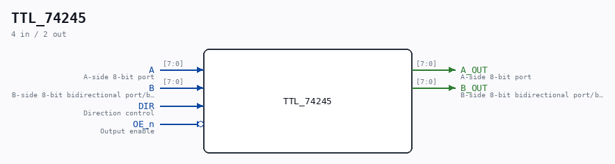
Schematic
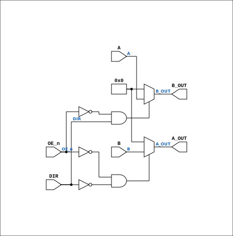
Drawn from the Verilog: the yosys netlist of the Simulation (Verilator) build, instance CORE.CPU_BOARD.CPU.PROC.CHIP_32F. Sub-modules are boxes (click the picture to open it full size; there every sub-module box links to its page, and every wire shows its Verilog name).
Description
Component : TTL_74245 Ronny Hansen 14.01.2024
Ports
| Direction | Width | Name | Description |
|---|---|---|---|
| input | [7:0] |
A |
A-side 8-bit port |
| output | [7:0] |
A_OUT |
A-side 8-bit port |
| input | [7:0] |
B |
B-side 8-bit bidirectional port/bus |
| output | [7:0] |
B_OUT |
B-side 8-bit bidirectional port/bus |
| input | 1 |
DIR |
Direction control |
| input | 1 |
OE_n (active low) |
Output enable |
Verilog source
Verilog/Shared/support/TTL_74245.v on GitHub.
Show the Verilog of TTL_74245 (49 lines)
/******************************************************************************
 **                                                                          **
 ** Component : TTL_74245                                                    **
 **                                                                          **
 ** Ronny Hansen 14.01.2024
 *****************************************************************************/

module TTL_74245(
    input  [7:0] A,        // A-side 8-bit port
    output [7:0] A_OUT,    // A-side 8-bit port

    input  [7:0] B,        // B-side 8-bit bidirectional port/bus
    output [7:0] B_OUT,    // B-side 8-bit bidirectional port/bus

    input DIR,           // Direction control
    input OE_n           // Output enable
);

    // NO SHARED HELPER WIRE HERE - this is deliberate, see below.
    //
    // The obvious way to write this part is
    //     wire [7:0] internalBus = DIR ? A : B;
    //     assign B_OUT = (!OE_n && DIR)  ? internalBus : 8'b0;
    //     assign A_OUT = (!OE_n && !DIR) ? internalBus : 8'b0;
    // which is FUNCTIONALLY correct - when DIR is 1 the helper is A, so B can
    // never reach B_OUT - but it creates the STRUCTURAL edge
    //     B -> internalBus -> B_OUT
    // and synthesis cannot know that DIR gates it. On a bidirectional bus
    // where the far end feeds back (FIDB: CGA_IDBCTL -> ALU_OUTMUX -> FIDBO ->
    // BusDriver16 -> here -> board IDB glue -> back to CGA_IDBCTL) that edge
    // closes a combinational LOOP.
    //
    // MEASURED 20-AUG-2026, Vivado 2025.2.1 on xc7a100t: 59 "[Synth 8-295]
    // found timing loop" warnings, each broken by an arbitrary inferred
    // set_disable_timing. The worst reported path then ran 181 logic levels /
    // 94.4 ns from an interrupt mask flip-flop to the WCS address input - but
    // 83.6 ns of that, 89%, was the tool walking ~14 LAPS around this loop,
    // one per bit position. It was never a real ND-120 signal path.
    //
    // Selecting the source directly per output is the same truth table with no
    // shared node, so the edge does not exist.
    assign B_OUT = (OE_n == 0 && DIR == 1) ? A : 8'b0;

    // Output to A when receiving from B with respect to OE (OE_n==1 means "isolated". Don't write to A or B)
    assign A_OUT = (OE_n == 0 && DIR == 0) ? B : 8'b0;

endmodule