CPU_15
Source: Verilog/CPU-BOARD-3202/circuit/CPU_15.v
Where it sits (Simulation): ND120_TOP > ND120_CORE > ND3202D > CPU_15
- instance path: CORE.CPU_BOARD.CPU
Used in: ND3202D (all tops)
Contains: CPU_CS_16, CPU_MMU_24, CPU_PROC_32
Module hierarchy - All modules
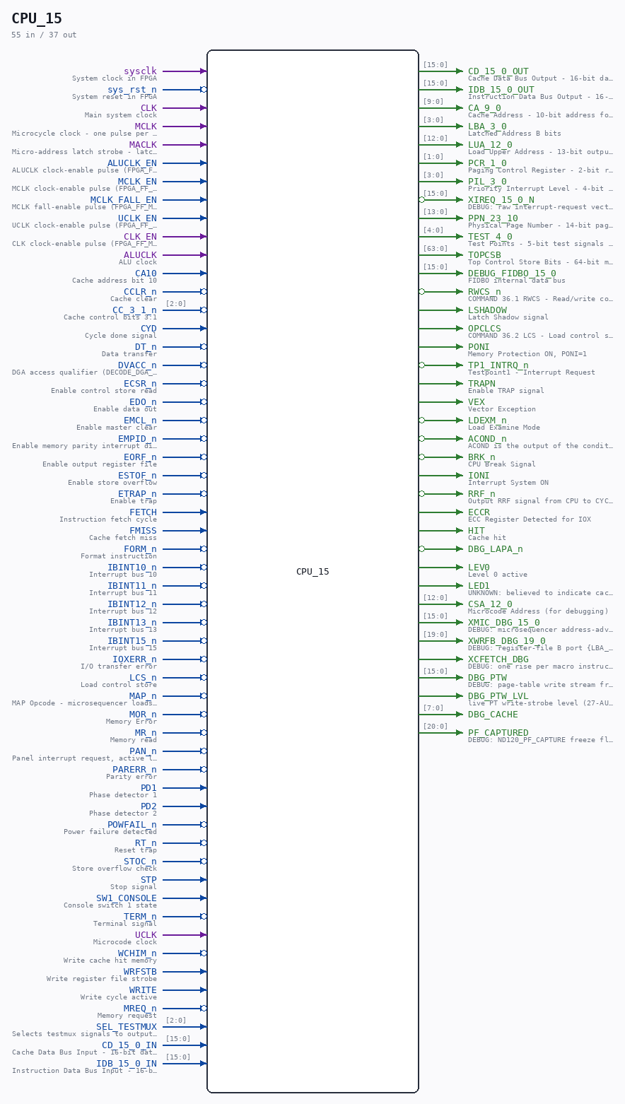
Schematic
Drawn from the Verilog: the yosys netlist of the Simulation (Verilator) build, instance CORE.CPU_BOARD.CPU. Sub-modules are boxes (click the picture to open it full size; there every sub-module box links to its page, and every wire shows its Verilog name).
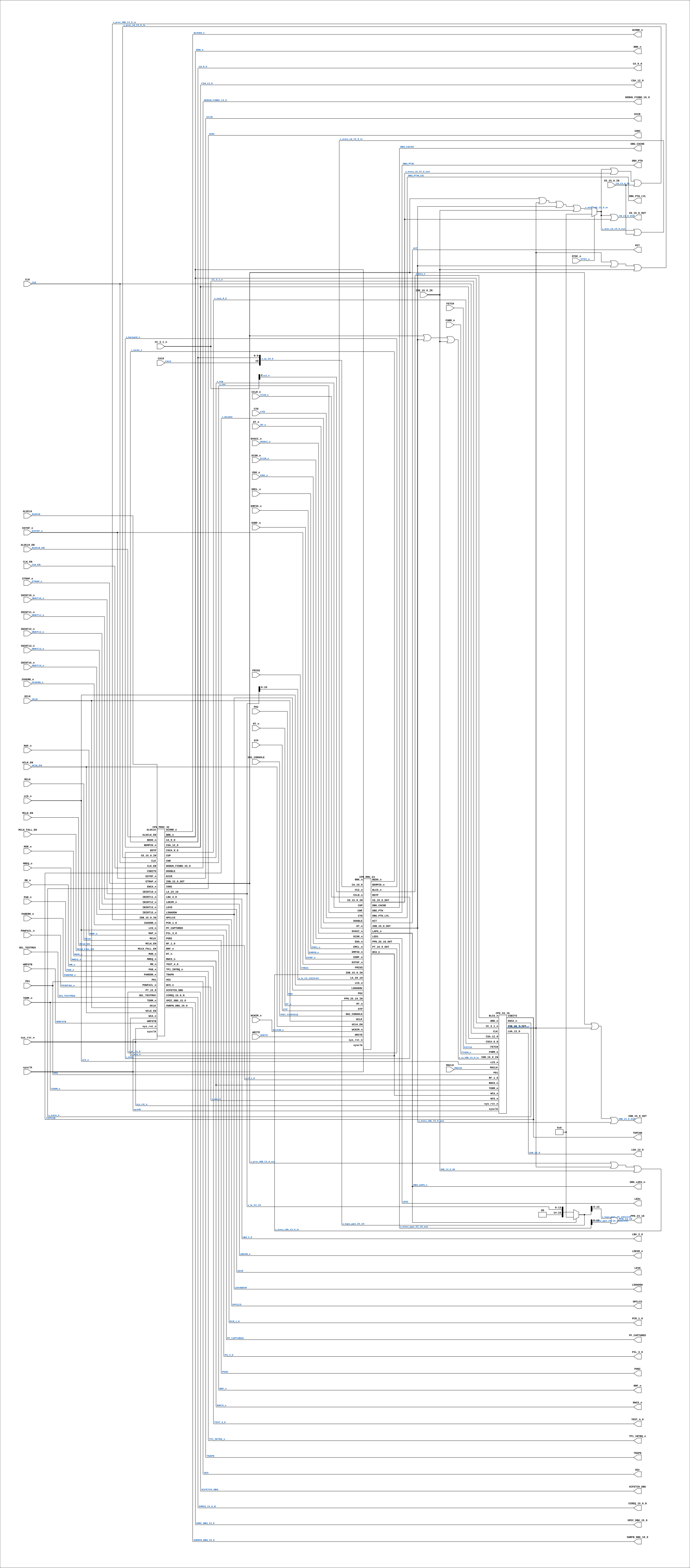
Description
ND120 CPU, MM&M CPU CPU TOP LEVEL SHEET 15 of 50 Last reviewed: 2-FEB-2025 Ronny Hansen
Ports
| Direction | Width | Name | Description |
|---|---|---|---|
| input | 1 |
sysclk |
System clock in FPGA |
| input | 1 |
sys_rst_n (active low) |
System reset in FPGA |
| input | 1 |
CLK |
Main system clock |
| input | 1 |
MCLK |
Microcycle clock - one pulse per microinstruction cycle (= TERM outside RWCS), stretched during RWCS. Not a master/memory clock. |
| input | 1 |
MACLK |
Micro-address latch strobe - latch enable for the control-store address latches in CPU_CS_ACAL_17 (transparent high, captures on the FALLING edge). NOT a memory clock. |
| input | 1 |
ALUCLK_EN |
ALUCLK clock-enable pulse (FPGA_FF_MODE, else 0) |
| input | 1 |
MCLK_EN |
MCLK clock-enable pulse (FPGA_FF_MODE, else 0) |
| input | 1 |
MCLK_FALL_EN |
MCLK fall-enable pulse (FPGA_FF_MODE, else 0) |
| input | 1 |
UCLK_EN |
UCLK clock-enable pulse (FPGA_FF_MODE, else 0) |
| input | 1 |
CLK_EN |
CLK clock-enable pulse (FPGA_FF_MODE, else 0) |
| input | 1 |
ALUCLK |
ALU clock |
| input | 1 |
CA10 |
Cache address bit 10 |
| input | 1 |
CCLR_n (active low) |
Cache clear |
| input | [2:0] |
CC_3_1_n (active low) |
Cache control bits 3:1 |
| input | 1 |
CYD |
Cycle done signal |
| input | 1 |
DT_n (active low) |
Data transfer |
| input | 1 |
DVACC_n (active low) |
DGA access qualifier (DECODE_DGA_COMM A227), passed down to CPU_MMU_24 - not the CGA's VACC |
| input | 1 |
ECSR_n (active low) |
Enable control store read |
| input | 1 |
EDO_n (active low) |
Enable data out |
| input | 1 |
EMCL_n (active low) |
Enable master clear |
| input | 1 |
EMPID_n (active low) |
Enable memory parity interrupt disable |
| input | 1 |
EORF_n (active low) |
Enable output register file |
| input | 1 |
ESTOF_n (active low) |
Enable store overflow |
| input | 1 |
ETRAP_n (active low) |
Enable trap |
| input | 1 |
FETCH |
Instruction fetch cycle |
| input | 1 |
FMISS |
Cache fetch miss |
| input | 1 |
FORM_n (active low) |
Format instruction |
| input | 1 |
IBINT10_n (active low) |
Interrupt bus 10 |
| input | 1 |
IBINT11_n (active low) |
Interrupt bus 11 |
| input | 1 |
IBINT12_n (active low) |
Interrupt bus 12 |
| input | 1 |
IBINT13_n (active low) |
Interrupt bus 13 |
| input | 1 |
IBINT15_n (active low) |
Interrupt bus 15 |
| input | 1 |
IOXERR_n (active low) |
I/O transfer error |
| input | 1 |
LCS_n (active low) |
Load control store |
| input | 1 |
MAP_n (active low) |
MAP Opcode - microsequencer loads next micro-address from the opcode mapper; last microinstruction of every macro instruction (active low) |
| input | 1 |
MOR_n (active low) |
Memory Error |
| input | 1 |
MR_n (active low) |
Memory read |
| input | 1 |
PAN_n (active low) |
Panel interrupt request, active low (from IO_37.PAN_n) |
| input | 1 |
PARERR_n (active low) |
Parity error |
| input | 1 |
PD1 |
Phase detector 1 |
| input | 1 |
PD2 |
Phase detector 2 |
| input | 1 |
POWFAIL_n (active low) |
Power failure detected |
| input | 1 |
RT_n (active low) |
Reset trap |
| input | 1 |
STOC_n (active low) |
Store overflow check |
| input | 1 |
STP |
Stop signal |
| input | 1 |
SW1_CONSOLE |
Console switch 1 state |
| input | 1 |
TERM_n (active low) |
Terminal signal |
| input | 1 |
UCLK |
Microcode clock |
| input | 1 |
WCHIM_n (active low) |
Write cache hit memory |
| input | 1 |
WRFSTB |
Write register file strobe |
| input | 1 |
WRITE |
Write cycle active |
| input | 1 |
MREQ_n (active low) |
Memory request |
| input | [2:0] |
SEL_TESTMUX |
Selects testmux signals to output on TEST_4_0 |
| input | [15:0] |
CD_15_0_IN |
Cache Data Bus Input - 16-bit data bus for transferring data between cache and CPU |
| output | [15:0] |
CD_15_0_OUT |
Cache Data Bus Output - 16-bit data bus for transferring data from CPU to cache |
| input | [15:0] |
IDB_15_0_IN |
Instruction Data Bus Input - 16-bit bidirectional bus for transferring instructions and data between CPU components |
| output | [15:0] |
IDB_15_0_OUT |
Instruction Data Bus Output - 16-bit bidirectional bus for transferring instructions and data from CPU components |
| output | [9:0] |
CA_9_0 |
Cache Address - 10-bit address for cache access |
| output | [3:0] |
LBA_3_0 |
Latched Address B bits |
| output | [12:0] |
LUA_12_0 |
Load Upper Address - 13-bit output for upper address bits of control store |
| output | [1:0] |
PCR_1_0 |
Paging Control Register - 2-bit register for paging control |
| output | [3:0] |
PIL_3_0 |
Priority Interrupt Level - 4-bit interrupt priority level |
| output | [15:0] |
XIREQ_15_0_N (active low) |
DEBUG: raw interrupt-request vector (active low) |
| output | [13:0] |
PPN_23_10 |
Physical Page Number - 14-bit page number for memory mapping |
| output | [4:0] |
TEST_4_0 |
Test Points - 5-bit test signals for debugging |
| output | [63:0] |
TOPCSB |
Top Control Store Bits - 64-bit microcode control signals |
| output | [15:0] |
DEBUG_FIDBO_15_0 |
FIDBO internal data bus |
| output | 1 |
RWCS_n (active low) |
COMMAND 36.1 RWCS - Read/write control store as addressed by ADCS command |
| output | 1 |
LSHADOW |
Latch Shadow signal |
| output | 1 |
OPCLCS |
COMMAND 36.2 LCS - Load control store from PROM and perform a Master Clear |
| output | 1 |
PONI |
Memory Protection ON, PONI=1 |
| output | 1 |
TP1_INTRQ_n (active low) |
Testpoint1 - Interrupt Request |
| output | 1 |
TRAPN |
Enable TRAP signal |
| output | 1 |
VEX |
Vector Exception |
| output | 1 |
LDEXM_n (active low) |
Load Examine Mode |
| output | 1 |
ACOND_n (active low) |
ACOND is the output of the condition register. |
| output | 1 |
BRK_n (active low) |
CPU Break Signal |
| output | 1 |
IONI |
Interrupt System ON |
| output | 1 |
RRF_n (active low) |
Output RRF signal from CPU to CYCLE |
| output | 1 |
ECCR |
ECC Register Detected for IOX |
| output | 1 |
HIT |
Cache hit |
| output | 1 |
DBG_LAPA_n (active low) |
|
| output | 1 |
LEV0 |
Level 0 active |
| output | 1 |
LED1 |
UNKNOWN: believed to indicate cache enabled, never traced. See Verilog/docs/SIGNALS.md |
| output | [12:0] |
CSA_12_0 |
Microcode Address (for debugging) |
| output | [15:0] |
XMIC_DBG_15_0 |
DEBUG: microsequencer address-advance probe (Tang 06000-hang) |
| output | [19:0] |
XWRFB_DBG_19_0 |
DEBUG: register-file B port {LBA_3_0, B_15_0} - STERR error number |
| output | 1 |
XCFETCH_DBG |
DEBUG: one rise per macro instruction (see CGA.v) |
| output | [15:0] |
DBG_PTW |
DEBUG: page-table write stream from CPU_MMU_24 (23-AUG, zero-read campaign) |
| output | 1 |
DBG_PTW_LVL |
live PT write-strobe level (27-AUG overlap probe) |
| output | [7:0] |
DBG_CACHE |
|
| output | [20:0] |
PF_CAPTURED |
DEBUG: ND120_PF_CAPTURE freeze flag (23-AUG) |
Verilog source
Verilog/CPU-BOARD-3202/circuit/CPU_15.v on GitHub.
Show the Verilog of CPU_15 (610 lines)
/**************************************************************************
** ND120 CPU, MM&M                                                       **
** CPU                                                                   **
** CPU TOP LEVEL                                                         **
** SHEET 15 of 50                                                        **
**                                                                       **
** Last reviewed: 2-FEB-2025                                             **
** Ronny Hansen                                                          **
***************************************************************************/


module CPU_15 (

    input sysclk,    // System clock in FPGA
    input sys_rst_n, // System reset in FPGA

    /*******************************************************************************
   ** The inputs are defined here                                                **
   *******************************************************************************/
    input CLK,          //! Main system clock
    input MCLK,         //! Microcycle clock - one pulse per microinstruction cycle (= TERM outside RWCS), stretched during RWCS. Not a master/memory clock.
    input MACLK,        //! Micro-address latch strobe - latch enable for the control-store address latches in CPU_CS_ACAL_17 (transparent high, captures on the FALLING edge). NOT a memory clock.
    input ALUCLK_EN,    //! ALUCLK clock-enable pulse (FPGA_FF_MODE, else 0)
    input MCLK_EN,      //! MCLK clock-enable pulse (FPGA_FF_MODE, else 0)
    input MCLK_FALL_EN, //! MCLK fall-enable pulse (FPGA_FF_MODE, else 0)
    input UCLK_EN,      //! UCLK clock-enable pulse (FPGA_FF_MODE, else 0)
    input CLK_EN,       //! CLK clock-enable pulse (FPGA_FF_MODE, else 0)
    input ALUCLK,       //! ALU clock

    input       CA10,         //! Cache address bit 10
    input       CCLR_n,       //! Cache clear
    input [2:0] CC_3_1_n,     //! Cache control bits 3:1

    input       CYD,          //! Cycle done signal
    input       DT_n,         //! Data transfer
    input       DVACC_n,      //! DGA access qualifier (DECODE_DGA_COMM A227), passed down to CPU_MMU_24 - not the CGA's VACC
    input       ECSR_n,       //! Enable control store read
    input       EDO_n,        //! Enable data out
    input       EMCL_n,       //! Enable master clear
    input       EMPID_n,      //! Enable memory parity interrupt disable
    input       EORF_n,       //! Enable output register file
    input       ESTOF_n,      //! Enable store overflow
    input       ETRAP_n,      //! Enable trap
    input       FETCH,        //! Instruction fetch cycle
    input       FMISS,        //! Cache fetch miss
    input       FORM_n,       //! Format instruction
    input       IBINT10_n,    //! Interrupt bus 10
    input       IBINT11_n,    //! Interrupt bus 11
    input       IBINT12_n,    //! Interrupt bus 12
    input       IBINT13_n,    //! Interrupt bus 13
    input       IBINT15_n,    //! Interrupt bus 15
    input       IOXERR_n,     //! I/O transfer error
    input       LCS_n,        //! Load control store
    input       MAP_n,        //! MAP Opcode - microsequencer loads next micro-address from the opcode mapper; last microinstruction of every macro instruction (active low)
    input       MOR_n,        //! Memory Error
    input       MR_n,         //! Memory read
    input       PAN_n,        //! Panel interrupt request, active low (from IO_37.PAN_n)
    input       PARERR_n,     //! Parity error
    input       PD1,          //! Phase detector 1
    input       PD2,          //! Phase detector 2
    input       POWFAIL_n,    //! Power failure detected
    input       RT_n,         //! Reset trap
    input       STOC_n,       //! Store overflow check
    input       STP,          //! Stop signal
    input       SW1_CONSOLE,  //! Console switch 1 state
    input       TERM_n,       //! Terminal signal
    input       UCLK,         //! Microcode clock
    input       WCHIM_n,      //! Write cache hit memory
    input       WRFSTB,       //! Write register file strobe
    input       WRITE,        //! Write cycle active
    input       MREQ_n,       //! Memory request
    input [2:0] SEL_TESTMUX,  //! Selects testmux signals to output on TEST_4_0
    /*******************************************************************************
   ** The signals with IN and OUT are defined here                               **
   *******************************************************************************/

    input  [15:0] CD_15_0_IN,    //! Cache Data Bus Input - 16-bit data bus for transferring data between cache and CPU
    output [15:0] CD_15_0_OUT,   //! Cache Data Bus Output - 16-bit data bus for transferring data from CPU to cache

    input  [15:0] IDB_15_0_IN,   //! Instruction Data Bus Input - 16-bit bidirectional bus for transferring instructions and data between CPU components
    output [15:0] IDB_15_0_OUT,  //! Instruction Data Bus Output - 16-bit bidirectional bus for transferring instructions and data from CPU components


    /*******************************************************************************
   ** The outputs are defined here                                               **
   *******************************************************************************/
    output [ 9:0] CA_9_0,      //! Cache Address - 10-bit address for cache access
    output [ 3:0] LBA_3_0,     //! Latched Address B bits
    output [12:0] LUA_12_0,    //! Load Upper Address - 13-bit output for upper address bits of control store
    output [ 1:0] PCR_1_0,     //! Paging Control Register - 2-bit register for paging control
    output [ 3:0] PIL_3_0,     //! Priority Interrupt Level - 4-bit interrupt priority level
    output [15:0] XIREQ_15_0_N, //! DEBUG: raw interrupt-request vector (active low)
    output [13:0] PPN_23_10,   //! Physical Page Number - 14-bit page number for memory mapping
    output [ 4:0] TEST_4_0,    //! Test Points - 5-bit test signals for debugging
    output [63:0] TOPCSB,      //! Top Control Store Bits - 64-bit microcode control signals
    output [15:0] DEBUG_FIDBO_15_0,  //! FIDBO internal data bus

    output RWCS_n,       //! COMMAND 36.1 RWCS - Read/write control store as addressed by ADCS command
    output LSHADOW,      //! Latch Shadow signal
    output OPCLCS,       //! COMMAND 36.2 LCS - Load control store from PROM and perform a Master Clear
    output PONI,         //! Memory Protection ON, PONI=1
    output TP1_INTRQ_n,  //! Testpoint1 - Interrupt Request
    output TRAPN,        //! Enable TRAP signal
    output VEX,          //! Vector Exception
    output LDEXM_n,      //! Load Examine Mode
    output ACOND_n,      //! ACOND is the output of the condition register.
    output BRK_n,        //! CPU Break Signal
    output IONI,         //! Interrupt System ON
    output RRF_n,        //! Output RRF signal from CPU to CYCLE
    output ECCR,         //! ECC Register Detected for IOX
    output HIT,          //! Cache hit
    //! Page-address latch, active low - asserted while the MMU/cache lookup
    //! that HIT belongs to is happening. Exported purely so the operator panel
    //! can compute a hit RATE: HIT on its own is a level with no denominator,
    //! and hits-per-clock is not what the CACHE HIT RATE field means.
    output DBG_LAPA_n,
    output LEV0,         //! Level 0 active
    output LED1,         //! UNKNOWN: believed to indicate cache enabled, never traced. See Verilog/docs/SIGNALS.md
    output [12:0] CSA_12_0,     //! Microcode Address (for debugging)
    output [15:0] XMIC_DBG_15_0, //! DEBUG: microsequencer address-advance probe (Tang 06000-hang)
    output [19:0] XWRFB_DBG_19_0,   //! DEBUG: register-file B port {LBA_3_0, B_15_0} - STERR error number
    output        XCFETCH_DBG,   //! DEBUG: one rise per macro instruction (see CGA.v)
    output [15:0] DBG_PTW,      //! DEBUG: page-table write stream from CPU_MMU_24 (23-AUG, zero-read campaign)
    output DBG_PTW_LVL,  //! live PT write-strobe level (27-AUG overlap probe)
    //! DEBUG: cache-write gating bus, straight through from CPU_MMU_24. See
    //! the DBG_CACHE port comment there for the bit layout and the reason.
    output [7:0] DBG_CACHE,
    output [20:0]        PF_CAPTURED   //! DEBUG: ND120_PF_CAPTURE freeze flag (23-AUG)
);


// NOTE on signals s_rt_n and s_rwcs_m
//
//  s_rt_n - also output from CPU_PROC_32. Use from PCB top module as we dont have the latest code for PAL 44608A that generates this signal
//  s_rwcs_n - also output from CPU_PROC_32. Use from from PROC - PAL in PROC fixes decoding of the RWCS command


  /*******************************************************************************
   ** The wires are defined here                                                 **
   *******************************************************************************/
  wire [13:0] s_la_23_10;
  wire [ 3:0] s_lba_3_0;
  wire [63:0] s_csbits;
  wire [15:0] s_lapa_ppn_25_10;
  wire [ 4:0] s_test_4_0;
  wire [ 9:0] s_csca_9_0;
  wire [ 2:0] s_cc_3_1_n;
  wire [ 1:0] s_rf_1_0;
  wire [ 6:0] s_pt_15_9;
  wire [12:0] s_csa_12_0;
  wire [10:0] s_ca_10_0;
  wire [ 1:0] s_pcr_1_0;
  wire [ 3:0] s_pil_3_0;
  wire [12:0] s_lua_12_0;
  wire [15:0] s_stoc_cd_15_0_out;
  wire [15:0] s_proc_cd_15_0_in;
  wire [15:0] s_proc_IDB_15_0_in;
  wire [15:0] s_proc_IDB_15_0_out;
  wire [15:0] s_cs_IDB_15_0_in;
  wire [15:0] s_cs_IDB_15_0_out;

  wire        s_blcs_n;
  wire        s_brk_n;
  wire        s_rt_n;
  wire        s_ewca_n;
  wire [7:0]  s_dbg_cache;   //! cache-write gating bus from CPU_MMU_24
  wire        s_eorf_n;
  wire        s_wcs_n;
  wire        s_emcl_n;
  wire        s_lapa_n;
  wire        s_pan_n;
  wire        s_aluclk;
  wire        s_ibint13_n;
  wire        s_cup;
  wire        s_acond_n;
  wire        s_mor_n;
  wire        s_maclk;
  wire        s_opclcs;
  wire        s_trap_n;
  wire        s_rrf_n;
  wire        s_lcs_n;
  wire        s_ibint15_n;
  wire        s_pd2;
  wire        s_powfail_n;
  wire        s_term_n;
  wire        s_map_n;
  wire        s_etrap_n;
  wire        s_wrfstb;
  wire        s_mreq_n;
  wire        s_wchim_n;
  wire        s_lev0;
  wire        s_ibint10_n;
  wire        s_ibint12_n;
  wire        s_stoc_n;
  wire        s_cyd;
  wire        s_tp1_intr1_n;
  wire        s_bempid_n;
  wire        s_sw1_console;
  wire        s_empid_n;
  wire        s_edo_n;
  wire        s_cwr;
  wire        s_rwcs_n;
  wire        s_write;
  wire        s_stp;
  wire        s_ioxerr_n;
  wire        s_parerr_n;
  wire        s_ecsr_n;
  wire        s_cc2_n;
  wire        s_form_n;
  wire        s_clk;
  wire        s_uclk;
  wire        s_ioni;
  wire        s_ibint11_n;
  wire        s_bedo_n;
  wire        s_eccr;
  wire        s_pd1;
  wire        s_estof_n;
  wire        s_hit;
  wire        s_lshadow;
  wire        s_poni;
  wire        s_double;
  wire        s_cclr_n;
  wire        s_bstp;
  wire        s_wca_n;
  wire        s_dt_n;
  wire        s_fmiss;
  wire        s_fetch;
  wire        s_vex;
  wire        s_dvacc_n;
  wire        s_mr_n;
  wire        s_mclk;
  wire        s_led1;


  wire [15:0] s_cpu_cd_15_0_in;
  wire [15:0] s_cpu_cd_15_0_out;

  wire [15:0] s_mmu_cd_15_0_in;
  wire [15:0] s_mmu_cd_15_0_out;

  wire [15:0] s_mmu_idb_15_0_in;
  wire [15:0] s_mmu_idb_15_0_out;

  wire [15:0] s_mmu_ppn_25_10_in;
  wire [15:0] s_mmu_ppn_25_10_out;

  wire [13:0] s_cpu_ppn_23_10_out;

  wire [15:0] s_stoc_idb_15_0_in;

  /*******************************************************************************
   ** The module functionality is described here                                 **
   *******************************************************************************/

  /*******************************************************************************
   ** Here all wiring is defined                                                 **
   *******************************************************************************/
  assign s_cc2_n = s_cc_3_1_n[2];

  /*******************************************************************************
   ** Here all input connections are defined                                     **
   *******************************************************************************/
  assign s_cc_3_1_n[2:0] = CC_3_1_n;
  assign s_ca_10_0[10] = CA10;
  assign s_rt_n   = RT_n; // Use incomming RT_n signal (DONT use signal out from PROC as we are missing the latest code for the latest PAL)
  assign s_eorf_n = EORF_n;
  assign s_emcl_n = EMCL_n;
  assign s_pan_n = PAN_n;
  assign s_aluclk = ALUCLK;
  wire s_aluclk_en;
  assign s_aluclk_en = ALUCLK_EN;
  wire s_mclk_en;
  assign s_mclk_en = MCLK_EN;
  wire s_mclk_fall_en;
  assign s_mclk_fall_en = MCLK_FALL_EN;
  wire s_uclk_en;
  assign s_uclk_en = UCLK_EN;
  wire s_clk_en;
  assign s_clk_en = CLK_EN;
  assign s_ibint13_n = IBINT13_n;
  assign s_mor_n = MOR_n;
  assign s_maclk = MACLK;
  assign s_lcs_n = LCS_n;
  assign s_ibint15_n = IBINT15_n;
  assign s_pd2 = PD2;
  assign s_powfail_n = POWFAIL_n;
  assign s_term_n = TERM_n;
  assign s_map_n = MAP_n;
  assign s_etrap_n = ETRAP_n;
  assign s_wrfstb = WRFSTB;
  assign s_wchim_n = WCHIM_n;
  assign s_ibint10_n = IBINT10_n;
  assign s_ibint12_n = IBINT12_n;
  assign s_stoc_n = STOC_n;
  assign s_cyd = CYD;
  assign DBG_CACHE = s_dbg_cache;
  assign s_sw1_console = SW1_CONSOLE;
  assign s_empid_n = EMPID_n;
  assign s_edo_n = EDO_n;
  //assign s_rwcs_n            = RWCS_n; // use signal from PROC
  assign s_write = WRITE;
  assign s_stp = STP;
  assign s_ioxerr_n = IOXERR_n;
  assign s_parerr_n = PARERR_n;
  assign s_ecsr_n = ECSR_n;
  assign s_form_n = FORM_n;
  assign s_clk = CLK;
  assign s_uclk = UCLK;
  assign s_ibint11_n = IBINT11_n;
  assign s_pd1 = PD1;
  assign s_estof_n = ESTOF_n;
  assign s_cclr_n = CCLR_n;
  assign s_dt_n = DT_n;
  assign s_fmiss = FMISS;
  assign s_fetch = FETCH;
  assign s_dvacc_n = DVACC_n;
  assign s_mr_n = MR_n;
  assign s_mclk = MCLK;
  assign s_mreq_n = MREQ_n;

  assign s_cpu_cd_15_0_in = CD_15_0_IN;


  /*******************************************************************************
   ** Here all output connections are defined                                    **
   *******************************************************************************/
  assign CA_9_0 = s_ca_10_0[9:0];
  assign CD_15_0_OUT = s_cpu_cd_15_0_out[15:0];


  // OR together "z" signals to create a common bus for IDB_15_0
  assign IDB_15_0_OUT =
      s_proc_IDB_15_0_out[15:0] |
      s_cs_IDB_15_0_out[15:0]   |
      s_mmu_idb_15_0_out[15:0];

  assign s_stoc_idb_15_0_in =
      s_proc_IDB_15_0_out[15:0] |
      s_cs_IDB_15_0_out[15:0]   |
      s_mmu_idb_15_0_out[15:0]  |
      IDB_15_0_IN;

  assign s_mmu_idb_15_0_in = s_proc_IDB_15_0_out[15:0] | s_cs_IDB_15_0_out[15:0] |
      //      s_stoc_idb_15_0_out[15:0]  | (signal doesnt exist)
      IDB_15_0_IN;


  assign s_proc_IDB_15_0_in[15:0]  =
    s_cs_IDB_15_0_out[15:0]   |
    s_mmu_idb_15_0_out[15:0]  |
    IDB_15_0_IN[15:0];

  assign s_cs_IDB_15_0_in = s_proc_IDB_15_0_out[15:0] | s_mmu_idb_15_0_out[15:0] | IDB_15_0_IN;

  // OR together "z" signals to create a common bus for CD_15_0
  assign s_proc_cd_15_0_in = s_stoc_cd_15_0_out | s_mmu_cd_15_0_out | s_cpu_cd_15_0_in;
  assign s_mmu_cd_15_0_in = s_stoc_cd_15_0_out | s_cpu_cd_15_0_in;


  assign s_cpu_cd_15_0_out = s_stoc_cd_15_0_out | s_mmu_cd_15_0_out;
  // REMOVED 20-AUG-2026: 'assign s_cpu_cd_15_0_out = s_cpu_cd_15_0_out;'
  // It was a SECOND continuous driver on this wire (the line above is the
  // real one), and it drove the wire FROM ITSELF - a zero-logic
  // combinational loop. Two continuous assignments on one wire resolve to x
  // wherever they disagree, and this wire leaves the board as CD_15_0_OUT
  // (line 316). Nothing sourced a value through it that line 348 does not
  // already provide.

  // other signals

  assign RWCS_n = s_rwcs_n;

  assign LBA_3_0 = s_lba_3_0[3:0];
  assign LSHADOW = s_lshadow;
  assign LUA_12_0 = s_lua_12_0[12:0];
  assign OPCLCS = s_opclcs;
  assign PCR_1_0 = s_pcr_1_0[1:0];
  assign PIL_3_0 = s_pil_3_0[3:0];
  assign PONI = s_poni;
  assign PPN_23_10 = s_cpu_ppn_23_10_out[13:0];
  assign TEST_4_0 = s_test_4_0[4:0];
  assign TOPCSB = s_csbits[63:0];
  assign TP1_INTRQ_n = s_tp1_intr1_n;
  assign TRAPN = s_trap_n;
  assign VEX = s_vex;
  assign ACOND_n = s_acond_n;
  assign BRK_n = s_brk_n;
  assign IONI = s_ioni;
  assign RRF_n = s_rrf_n;
  assign ECCR = s_eccr;
  assign HIT = s_hit;
  assign DBG_LAPA_n = s_lapa_n;
  assign LEV0 = s_lev0;

  assign LED1 = s_led1;
  assign CSA_12_0 = s_csa_12_0;

  /*******************************************************************************
   ** Here all sub-circuits are defined                                          **
   *******************************************************************************/


  /****** CPU_STOC_35.v is replaced by this line below ******/
  // If STOC_n is high, output is high-impedance
  // (Its a buffer, so it only forwards data from IDB to STOC_cd_15_out)
  assign s_stoc_cd_15_0_out[15:0] = s_stoc_n ? 16'b0 : s_stoc_idb_15_0_in[15:0];

  /****** CPU_LAPA_23.v is replaced by this line below ******/
  // is s_lapa_n is high, output is high-impedance
  assign s_lapa_ppn_25_10[15:0] = s_lapa_n ? 16'b0 : {2'b0, s_la_23_10[13:0]};

  assign s_mmu_ppn_25_10_in = s_lapa_ppn_25_10;  // PPN Input to MMU

  assign s_cpu_ppn_23_10_out[13:0] = s_lapa_ppn_25_10[13:0] | s_mmu_ppn_25_10_out[13:0];

  // Code to make LINTER not complaing about bits _not_ read in s_mmu_ppn_25_10_out 15:14
  (* keep = "true", DONT_TOUCH = "true" *) wire [1:0] unused_MMU_PPN_bits;
  assign unused_MMU_PPN_bits[1:0] =  s_mmu_ppn_25_10_out[15:14];


  CPU_PROC_32 PROC
  (
    .sysclk(sysclk),  // System clock in FPGA
    .sys_rst_n(sys_rst_n),  // System reset in FPGA

    // Input signals
    .ALUCLK_EN(s_aluclk_en),
    .MCLK_EN(s_mclk_en),
    .MCLK_FALL_EN(s_mclk_fall_en),
    .UCLK_EN(s_uclk_en),
    .CLK_EN(s_clk_en),
    .ALUCLK(s_aluclk),
    .BEDO_n(s_bedo_n),
    .BEMPID_n(s_bempid_n),
    .CD_15_0_IN(s_proc_cd_15_0_in[15:0]),
    .CLK(s_clk),
    .CSBITS(s_csbits[63:0]),
    .CSCA_9_0(s_csca_9_0[9:0]),
    .ESTOF_n(s_estof_n),
    .ETRAP_n(s_etrap_n),
    .EWCA_n(s_ewca_n),
    .IBINT10_n(s_ibint10_n),
    .IBINT11_n(s_ibint11_n),
    .IBINT12_n(s_ibint12_n),
    .IBINT13_n(s_ibint13_n),
    .IBINT15_n(s_ibint15_n),
    .IOXERR_n(s_ioxerr_n),
    .LCS_n(s_lcs_n),
    .MAP_n(s_map_n),
    .MCLK(s_mclk),
    .MOR_n(s_mor_n),
    .MREQ_n(s_mreq_n),
    .MR_n(s_mr_n),
    .PAN_n(s_pan_n),
    .PARERR_n(s_parerr_n),
    .PD1(s_pd1),
    .POWFAIL_n(s_powfail_n),
    .PT_15_9(s_pt_15_9[6:0]),  // Page Table bits 15:9 in to CGA/Delilah
    .TERM_n(s_term_n),
    .SEL_TESTMUX(SEL_TESTMUX),
    .UCLK(s_uclk),
    .WCA_n(s_wca_n),
    .WRFSTB(s_wrfstb),

    // Input and output bus signals
    .IDB_15_0_IN(s_proc_IDB_15_0_in[15:0]),
    .IDB_15_0_OUT(s_proc_IDB_15_0_out[15:0]),

    // Output Signals
    .BSTP(s_bstp),
    .ACOND_n(s_acond_n),  //Output: connected to top and then CYC
    .BRK_n(s_brk_n),
    .CA_9_0(s_ca_10_0[9:0]),
    .CSA_12_0(s_csa_12_0[12:0]),
    .CUP(s_cup),
    .CWR(s_cwr),
    .DOUBLE(s_double),
    .ECCR(s_eccr),  //Output
    .IONI(s_ioni),  //Output
    .LA_23_10(s_la_23_10[13:0]),
    .LBA_3_0(s_lba_3_0[3:0]),
    .LEV0(s_lev0),
    .LSHADOW(s_lshadow),
    .OPCLCS(s_opclcs),
    .PCR_1_0(s_pcr_1_0[1:0]),
    .PIL_3_0(s_pil_3_0[3:0]),
    .XIREQ_15_0_N(XIREQ_15_0_N),
    .PONI(s_poni),
    .RF_1_0(s_rf_1_0[1:0]),
    .RRF_n(s_rrf_n),  //Output
    .RT_n(),  // Dont use this output signal as its locked to 1/HIGH (missing latest PALASM code for 44608A)

    .LDEXM_n(LDEXM_n),
    .RWCS_n(s_rwcs_n),  // RWCS signal fixed in PAL. Was wrongly decoded in DGA
    .TEST_4_0(s_test_4_0[4:0]),
    .TP1_INTRQ_n(s_tp1_intr1_n),
    .TRAPN(s_trap_n),  // TRAP_n output
    .VEX(s_vex),
    .WCS_n(s_wcs_n),

    .DEBUG_FIDBO_15_0(DEBUG_FIDBO_15_0),
    .XMIC_DBG_15_0(XMIC_DBG_15_0),
    .XWRFB_DBG_19_0(XWRFB_DBG_19_0),
      .XCFETCH_DBG(XCFETCH_DBG),
    .PF_CAPTURED(PF_CAPTURED)
  );

  CPU_CS_16 CS (
      .sysclk   (sysclk),    // System clock in FPGA
      .sys_rst_n(sys_rst_n), // System reset in FPGA

      /* Clock signals */
      .CLK  (s_clk),
      .MACLK(s_maclk),

      /* Test signals */
      .PD1(s_pd1),

      /* Input signals */
      .IDB_15_0_IN(s_cs_IDB_15_0_in[15:0]),

      .BLCS_n(s_blcs_n),
      .BRK_n(s_brk_n),
      .CC_3_1_n(s_cc_3_1_n[2:0]),
      .CSA_12_0(s_csa_12_0[12:0]),
      .CSCA_9_0(s_csca_9_0[9:0]),
      .FETCH(s_fetch),
      .FORM_n(s_form_n),
      .LCS_n(s_lcs_n),
      .RF_1_0(s_rf_1_0[1:0]),
      .RWCS_n(s_rwcs_n),
      .TERM_n(s_term_n),
      .WCA_n(s_wca_n),
      .WCS_n(s_wcs_n),

      /* OUTPUTS */
      .EWCA_n(s_ewca_n),
      .CSBITS(s_csbits[63:0]),
      .IDB_15_0_OUT(s_cs_IDB_15_0_out[15:0]),
      .LUA_12_0(s_lua_12_0[12:0])
  );

  CPU_MMU_24 MMU
  (
    // FPGA system signals
    .sysclk   (sysclk),    // System clock in FPGA
    .sys_rst_n(sys_rst_n), // System reset in FPGA

    // Input signals
    .BRK_n(s_brk_n),
    .CA_10_0(s_ca_10_0[10:0]),
    .CC2_n(s_cc2_n),
    .CCLR_n(s_cclr_n),
    .CUP(s_cup),
    .CWR(s_cwr),
    .CYD(s_cyd),
    .DOUBLE(s_double),
    .DT_n(s_dt_n),
    .DVACC_n(s_dvacc_n),
    .ECSR_n(s_ecsr_n),
    .EDO_n(s_edo_n),
    .EMCL_n(s_emcl_n),
    .EMPID_n(s_empid_n),
    .EORF_n(s_eorf_n),
    .ESTOF_n(s_estof_n),
    .FMISS(s_fmiss),
    .LA_20_10(s_la_23_10[10:0]),
    .LCS_n(s_lcs_n),
    .LSHADOW(s_lshadow),
    .PD2(s_pd2),
    .RT_n(s_rt_n),
    .STP(s_stp),
    .SW1_CONSOLE(s_sw1_console),
    .UCLK(s_uclk),
    .UCLK_EN(s_uclk_en),
    .WCHIM_n(s_wchim_n),
    .WRITE(s_write),

    // Bus signals
    .IDB_15_0_IN(s_mmu_idb_15_0_in[15:0]),
    .IDB_15_0_OUT(s_mmu_idb_15_0_out[15:0]),

    .CD_15_0_IN(s_mmu_cd_15_0_in[15:0]),
    .CD_15_0_OUT(s_mmu_cd_15_0_out[15:0]),

    .PPN_25_10_IN(s_mmu_ppn_25_10_in[15:0]),
    .PPN_25_10_OUT(s_mmu_ppn_25_10_out[15:0]),

    // Output signals
    .BEDO_n(s_bedo_n),
    .BEMPID_n(s_bempid_n),
    .BLCS_n(s_blcs_n),
    .BSTP(s_bstp),

    .HIT(s_hit),
    .LAPA_n(s_lapa_n),
    .PT_15_9_OUT(s_pt_15_9[6:0]),
    .WCA_n(s_wca_n),
    .LED1(s_led1),
    .DBG_PTW(DBG_PTW),
      .DBG_PTW_LVL(DBG_PTW_LVL),
      .DBG_CACHE(s_dbg_cache)   // cache-write gating bus, see the port comment
  );


endmodule